

SGS Thomson Microelectronics M24C02-S, M24C04-S, M24C08-S, M24C02-L, M24C01-S Datasheet
...
1/26May 2003
M24C16, M24C08
M24C04, M24C02, M24C01
16Kbit, 8Kbit, 4Kbit, 2Kbit and 1Kbit Serial I²C Bus EEPROM
FEATURES SUMMARY
■ Two Wire I
2
C Serial Interface
Supports 400 kHz Protocol
■ Single Supply Voltage:
– 4.5V to 5.5V for M24Cxx
– 2.5V to 5.5V for M24Cxx-W
– 2.2V to 5.5V for M24Cxx-L
– 1.8V to 5.5V for M24Cxx-R
■ Write Control Input
■ BYTE and PAGE WRITE (up to 16 Bytes)
■ RANDOM and SEQUENTIAL READ Modes
■ Self-Timed Pro gr amming Cyc le
■ Automatic Address Incrementing
■ Enhanced ESD/Latch-Up Behavior
■ More than 1 Million Erase/Write Cycles
■ More than 40 Year Data Retention
Figure 1. Packages
PDIP8 (BN)
8
1
SO8 (MN)
150 mil width
8
1
TSSOP8 (DW)
169 mil width
TSSOP8 (DS)
3x3mm² body size (MSOP)
M24C16, M24C08, M24C04, M24C02, M24C01
2/26
SUMMARY DESCRIPTION
These I
2
C-compatible electrically erasable
programmable memory (EEPROM) devices are
organized as 2048/1024/512/256/128 x 8
(M24C16, M24C08, M24C04, M24C02, M24C01).
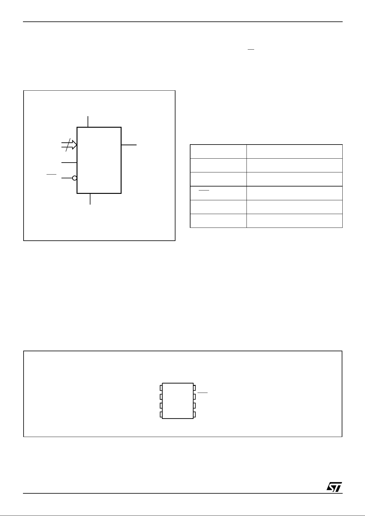
Figure 2. L o gi c Diag ram
These devices are compatible with the I
2
C memory protocol. This is a two wi re serial interface that
uses a bi-directional data bus and serial clock. The
devices carry a built-in 4-bit Device Type Identifier
code (1010) in accordance with the I
2
C bus defini-
tion.
The device behaves as a slave in the I
2
C protocol,
with all memory operations synchronized by the
serial clock. Read and Write operations are initiated by a Start condition, generated by the bus mas-
ter. The Start condition is followed by a Device
Select Code and RW
bit (as described in Table 2),
terminated by an acknowledge bit.
When writing data to the memory, the device in-
serts an acknowledge bit during the 9
th
bit time,
following the bus master’s 8-bit transmission.
When data is read by the bus master, the bus
master acknowledg es t he rec eipt of the data b yte
in the same way. Data transfers are terminated by
a Stop condition after an Ack for Write, and after a
NoAck for Read.
Table 1. Signal Names
Power On Reset: V
CC
Lock-Out Write Protect
In order to prevent data corruption and inadvertent
Write operations during Power-up, a Power On
Reset (POR) circuit is included. The internal reset
is held active until V
CC
has reached the POR
threshold value, and all operations are disabled –
the device will not respond to any command. In the
same way, when V
CC
drops from the operating
voltage, below the POR threshold value , all operations are disabled and the device will not respond
to any command. A stable and valid V
CC
must be
applied before applying any logic signal.
Figure 3. DIP, SO and TSSOP Connections
Note: 1. NC = Not Connected
2. See page 20 (onwards) f or package di m ensions , an d how to identify pin-1.
AI02033
3
E0-E2 SDA
V
CC
M24Cxx
WC
SCL
V
SS
E0, E1, E2 Chip Enable
SDA Serial Data
SCL Serial Clock
WC
Write Control
V
CC
Supply Voltage
V
SS
Ground
SDAV
SS
SCL
WC
V
CC
/ E2
AI02034E
M24Cxx
1
2
3
4
8
7
6
5
/ E2/ E2/ E2NC
/ E1
/ E1/ E1/ NCNC
/ E0
/ E0/ NC/ NCNC
/1Kb
/2Kb/4Kb/8Kb16Kb
3/26
M24C16, M24C08, M24C04, M 24C02, M24C01
SIGNAL DESCRIPTION
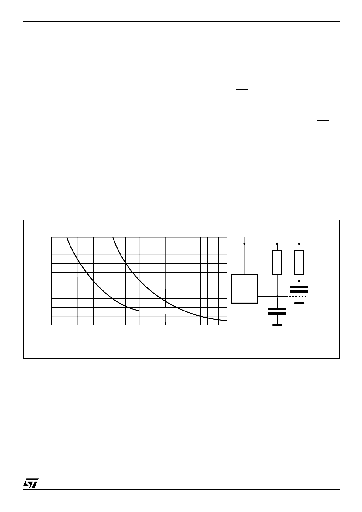
Serial Clock (SCL)
This input signal is u sed to strobe all data in and
out of the device. In applications where this signal
is used by slave devices to synchronize the bus to
a slower clock, the bus master must have an open
drain output, and a pull-up resistor can be connected from Serial Clock (SCL) to V
CC
. (Figure 4
indicates how the valu e of the pull-up resist or can
be calculated). In most applications , though, this
method of synchronization is no t employed, and
so the pull-up resistor is not necessary, provided
that the bus maste r has a push-pull (rather than
open drain) output.
Serial Data (SDA)
This bi-directional signal is used to transfer data in
or out of the device. It is an open drain output that
may be wire-OR’ed with ot her op en drai n or open
collector signals on the bus. A pull up resistor must
be connected from Serial Data (SDA) to V
CC
. (Figure 4 indicates how the value of the pull-up resistor
can be calculated).
Chip Enable (E0, E1, E2)
These input signals are used to set the value that
is to be looked for on the three least significant bits
(b3, b2, b1) of the 7-bit Device Select Code. These
inputs must be tied to V
CC
or VSS, to establish the
Device Select Code.
Write Control (WC
)
This input signal is useful for protecting the entire
contents of the memory from inadvertent write operations. Write operations are disabled to the entire memory array when Write Control (WC
) is
driven High. When unconnected, the signal is internally read as V
IL
, and Write operations are al-
lowed.
When Write Control (WC
) is driven High, Device
Select and Address bytes are acknowledged,
Data bytes are not acknowledged.
Figure 4. Maximum R
L
Value versus Bus Capacitance (C
BUS
) for an I2C Bus
AI01665
V
CC
C
BUS
SDA
R
L
MASTER
R
L
SCL
C
BUS
100
0
4
8
12
16
20
C
BUS
(pF)
Maximum RP value (kΩ)
10 1000
fc = 400kHz
fc = 100kHz
M24C16, M24C08, M24C04, M24C02, M24C01
4/26
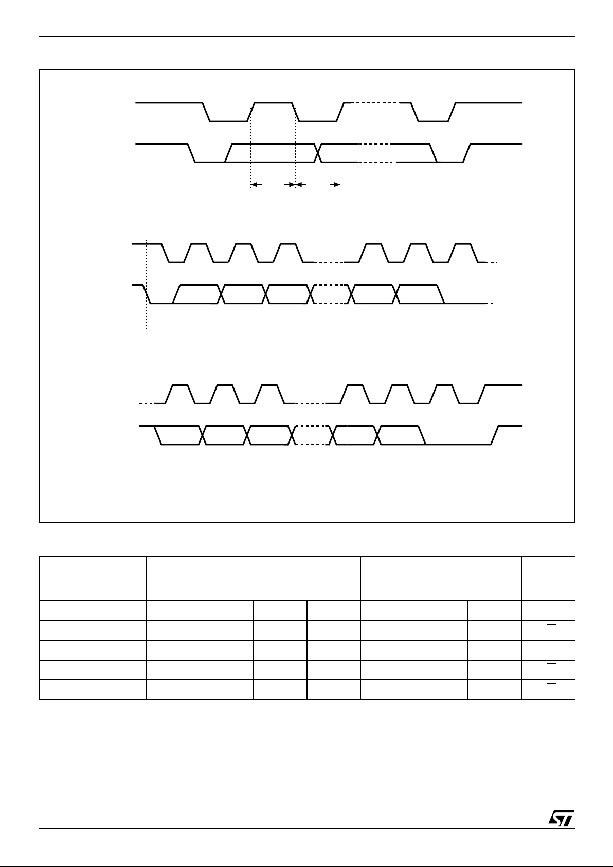
Figure 5. I2C Bus Protocol
Table 2. Device Select Code
Note: 1. The mos t si gnificant bit, b7, is sent first .
2. E0, E1 and E2 are compared against the respe ct i ve external pins on th e m em ory devi ce.
3. A10, A9 and A8 repres ent most signif i cant bits of th e address.
Device Type Identifier
1
Chip Enable
2,3
RW
b7
b6 b5 b4 b3 b2 b1 b0
M24C01 Select Code 1010E2E1E0RW
M24C02 Select Code 1010E2E1E0RW
M24C04 Select Code 1010E2E1A8RW
M24C08 Select Code 1010E2A9A8RW
M24C16 Select Code 1010A10A9A8RW
SCL
SDA
SCL
SDA
SDA
START
Condition
SDA
Input
SDA
Change
AI00792B
STOP
Condition
1 23 789
MSB
ACK
START
Condition
SCL
1 23 789
MSB ACK
STOP
Condition

5/26
M24C16, M24C08, M24C04, M 24C02, M24C01
DEVICE OPERATION
The device supports the I
2
C proto col. This is summarized in Figure 5. Any device that sends data on
to the bus is defined to be a transmi tter, and any
device that reads the data to be a receiver. The
device that controls the data trans fer is known as
the bus master, and the other as the slave device.
A data transfer can only be initiated by the bus
master , w hic h w ill also provide t he s er ial cloc k f or
synchronization. The M24Cxx device is always a
slave in all communication.
Start Condition
Start is identified by a falling edge of Serial Data
(SDA) while Serial Clock (SCL) is stable in the
High state. A Start condition must precede any
data transfer command. The dev ice continuously
monitors (except during a Write cycle) Serial Data
(SDA) and Serial Clock (SCL) for a Start condition,
and will not respond unless one is given.
Stop Condition
Stop is identified by a rising edg e of Serial Data
(SDA) while Serial Clock (SCL) is stable and driven High. A Stop condition terminates communication between the device and the bus master. A
Read command that is followed by NoAck can be
followed by a Stop condition to force the device
into the Stand-by mode. A Stop condition at the
end of a Write command triggers th e internal EEPROM W r ite cycle.
Acknowledge Bit (ACK)
The acknowledge bit is used to indicate a successful byte transfer. The bus transmitter, whether it be
bus master or slave device, releases Serial Data
(SDA) after sending eight bits of data. During the
9
th
clock pulse period, the receiver pulls Serial
Data (SDA) Low to acknowledge the receipt of the
eight data bits.
Data Input
During data input, the device samples Serial Data
(SDA) on the rising edge of Serial Clock (SCL).
For correct device operation, Serial Data (SDA)
must be stable during the rising edge of Serial
Clock (SCL), and the Serial Data (SDA) signal
must change
only
when Serial Clock (SCL) is driv-
en Low.
Memory Addressing
To start communication be tween the bus master
and the slave device, the bus m aste r must initiate
a Start condition. Following this, the bus master
sends the Device Select Code, shown i n Table 2
(on Serial Data (SDA), most significant bit first).
The Device Select Code consists of a 4-bit Device
Type Identifier, and a 3-bit Chip Enable “Address”
(E2, E1, E0). To address the memory array, the 4bit Device Type Identifier is 1010b.
When the Device Select Code is received on Serial Data (SDA), the device only responds if the Chip
Enable Address is the same as the value on the
Chip Enable (E0, E1, E2) inputs.
The 8
th
bit is the Read/Write bit (RW). This bit is
set to 1 for Read and 0 for Write operations.
If a match occurs on the Device Select code , the
corresponding device gives an acknowledgment
on Serial Data (SDA) during the 9
th
bit time. If the
device does not match the Device Select code, it
deselects itself from the bus, and goes into Standby mode.
Devices with larger memory capacities (the
M24C16, M24C08 and M24C04) need more address bits. E0 i s not available f or use on dev ices
that need to use address line A8; E1 is not available for devices that need to use addres s line A9,
and E2 is not available for devices that need to use
address line A10 (see Figure 3 and Table 2 for details). Using the E0, E1 and E2 inputs pins, up to
eight M24C02 (or M24C01), four M24C04, two
M24C08 or one M24C16 device can be connected
to one I
2
C bus. In each case, and in the hybrid cases, this gives a total memory capacity of 16 Kbits,
2 KBytes (except where M24C01 devices are
used).
Table 3. Operating Modes
Note: 1. X = V
IH
or V
IL
.
Mode RW bit
WC
1
Bytes Initial Sequence
Current Address Read 1 X 1 START, Device Select, RW
= 1
Random Address Read
0X
1
START, Device Select, RW
= 0, Address
1 X reSTART, Device Select, RW
= 1
Sequential Read 1 X
≥
1 Similar to Current or Random Address Read
Byte Write 0
V
IL
1 START, Device Select, RW = 0
Page Write 0
V
IL
≤
16 START, Device Select, RW
= 0
M24C16, M24C08, M24C04, M24C02, M24C01
6/26
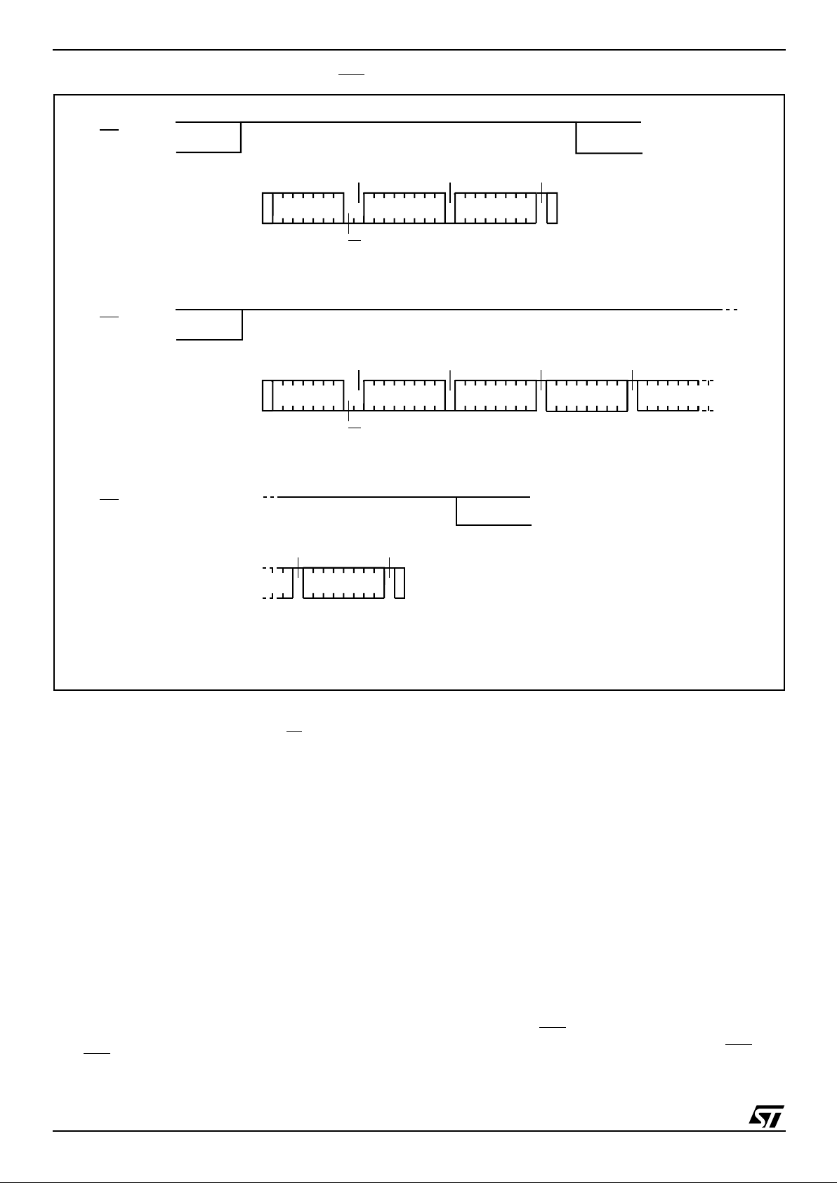
Figure 6. Wri t e Mo de S equences with WC=1 (data write inhibi ted)
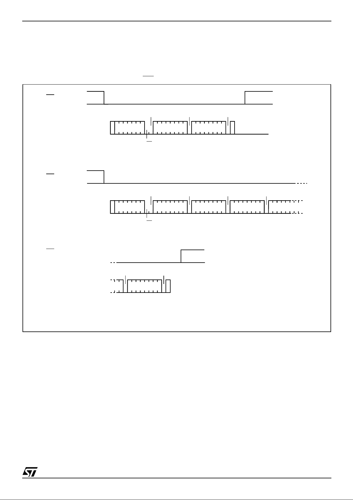
Write Operations
Following a Start condition the bus master s ends
a Device Select Code with the RW
bit rese t to 0.
The device acknowledges this, as shown in Figure
7, and waits for an address byte. The device responds to the address byte with an ack nowledge
bit, and then waits for the data byte.
When the bus master generate s a Stop c ondition
immediately after the Ack bi t (in the “10
th
bit” time
slot), either at the end of a Byte Write or a Page
Write, the internal memory Write cycle is triggered.
A Stop condition at any other time slot does not
trigger the internal Write cycle.
During the internal Write cycle, Seria l Data (SDA)
and Serial Clock (SCL) are ignored, and t he device does not respond to any requests.
Byte Write
After the Device Select code and the address byte,
the bus master sends one data byte. If the addressed location is Write-protected, by Write Control (WC
) being driven High (during the period from
the Start condition until the end of the address
byte), the device replies to the data byte with
NoAck, as shown in Figure 6, and the location is
not modified. If, instead, the addressed location is
not Write-protected, the device replies with Ack.
The bus master terminates the transf er by generating a Stop condition, as shown in Figure 7.
Page Write
The Page Write mode allows u p to 16 byt es to be
written in a single Write cycle, provided that they
are all located in the same page in the memory:
that is, the most significant memory address bits
are the same. If more bytes are sent than will fit up
to the end of t he pa ge, a condition known as ‘ rollover’ occurs. This should be avoided, as data
starts to become overwritten in an implementation
dependent way.
The bus master s ends f rom 1 to 16 bytes of data,
each of which is acknowledged by the device if
Write Control (WC
) is Low. If the addressed loca-
tion is Write-protected, by Write Control (WC
) be-
ing driven High (during the period from the S tart
STOP
START
Byte Write DEV SEL BYTE ADDR DATA IN
WC
START
Page Write DEV SEL BYTE ADDR DATA IN 1 DATA IN 2
WC
DATA IN 3
AI02803C
Page Write
(cont'd)
WC (cont'd)
STOP
DATA IN N
ACK ACK NO ACK
R/W
ACK ACK NO ACK NO ACK
R/W
NO ACK NO ACK
7/26
M24C16, M24C08, M24C04, M 24C02, M24C01
condition until the end of the address byte), the device replies to the data bytes with NoAck, as
shown in Figure 6, and the locations are not modified. After each byte is transferred, the internal
byte address counter (the 4 least significant address bits only) is incremented. The transfer i s t erminated by the bus master generating a Stop
condition.
Figure 7. Wri t e Mo de S equences with W
C=0 (data write enabled)
STOP
START
BYTE WRITE DEV SEL BYTE ADDR DATA IN
WC
START
PAGE WRITE DEV SEL BYTE ADDR DATA IN 1 DATA IN 2
WC
DATA IN 3
AI02804B
PAGE WRITE
(cont'd)
WC (cont'd)
STOP
DATA IN N
ACK
R/W
ACK ACK
ACK ACK ACK ACK
R/W
ACKACK
M24C16, M24C08, M24C04, M24C02, M24C01
8/26
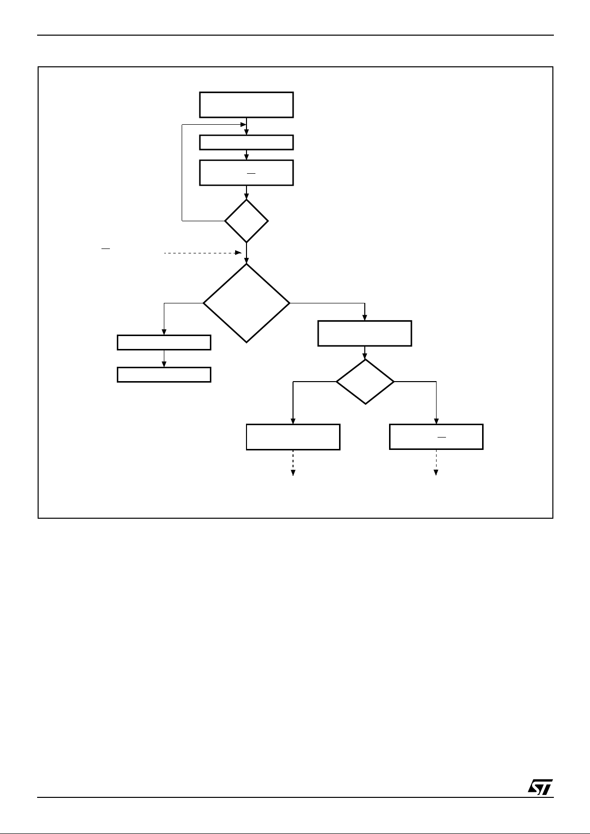
Figure 8. Wri t e C yc le Polling Flowc ha rt us i n g A C K
Minimizing System Delays by Polling On ACK
During the internal Write cycle, the device disconnects itself from the bus, and writes a copy of the
data from its internal latches to the memo ry cells.
The maximum Write time (t
w
) is shown in T ables
19 to 21, bu t the typical time is shorter. To m ake
use of this, a polling sequence can be used by the
bus master.
The sequence, as shown in Figure 8, is:
– Initial condition: a Write cycle is in progress.
– Step 1: the bus ma ster issues a Start condition
followed by a Device Select Code (the first byte
of the new instruction).
– Step 2: if the device is busy with the internal
Write cycle, no Ack will be returned and the bus
master goes back to Step 1. If the device has
terminated the internal Write cycle, it responds
with an Ack, indicating that the device is ready
to receive the second part of the instruction (the
first byte of this instruction having been sent
during Step 1).
WRITE Cycle
in Progress
AI01847C
Next
Operation is
Addressing the
Memory
START Condition
DEVICE SELECT
with RW = 0
ACK
Returned
YES
NO
YESNO
ReSTART
STOP
DATA for the
WRITE Operation
DEVICE SELECT
with RW = 1
Send Address
and Receive ACK
First byte of instruction
with RW = 0 already
decoded by the device
YESNO
START
Condition
Continue the
WRITE Operation
Continue the
Random READ Operation
 Loading...