

1/20
PRELIMINARY DATA
April 2000
This is preliminary information on a new product now in development or undergoing evaluation. Details are subject to change without notice.
M24256-A
256 Kbit SerialI C Bus EEPROM
With Two Chip Enable Lines
■ Compatible with I
2
C Extended Addressing
■ Two Wire I
2
C Serial Interface
Supports 400 kHz Protocol
■ Single Supply Voltage:
– 4.5V to 5.5V for M24256-A
– 2.5V to 5.5V for M24256-AW
– 1.8V to 3.6V for M24256-AR
■ 2 Chip Enable Inputs: up to four memories can
be connected to the same I2C bus
■ Hardware Write Control
■ BYTE and PAGE WRITE (up to 64 Bytes)
■ RANDOM and SEQUENTIAL READ Modes
■ Self-Timed Programming Cycle
■ Automatic Address Incrementing
■ Enhanced ESD/Latch-Up Behavior
■ More than 100,000 Erase/Write Cycles
■ More than 40 Year Data Retention
DESCRIPTION
These I2C-compatible electrically erasable programmable memory (EEPROM) devices are organized as 32Kx8 bits, and operate down to 2.5 V
(for the M24256-AW), and down to 1.8 V (for the
M24256-AR).
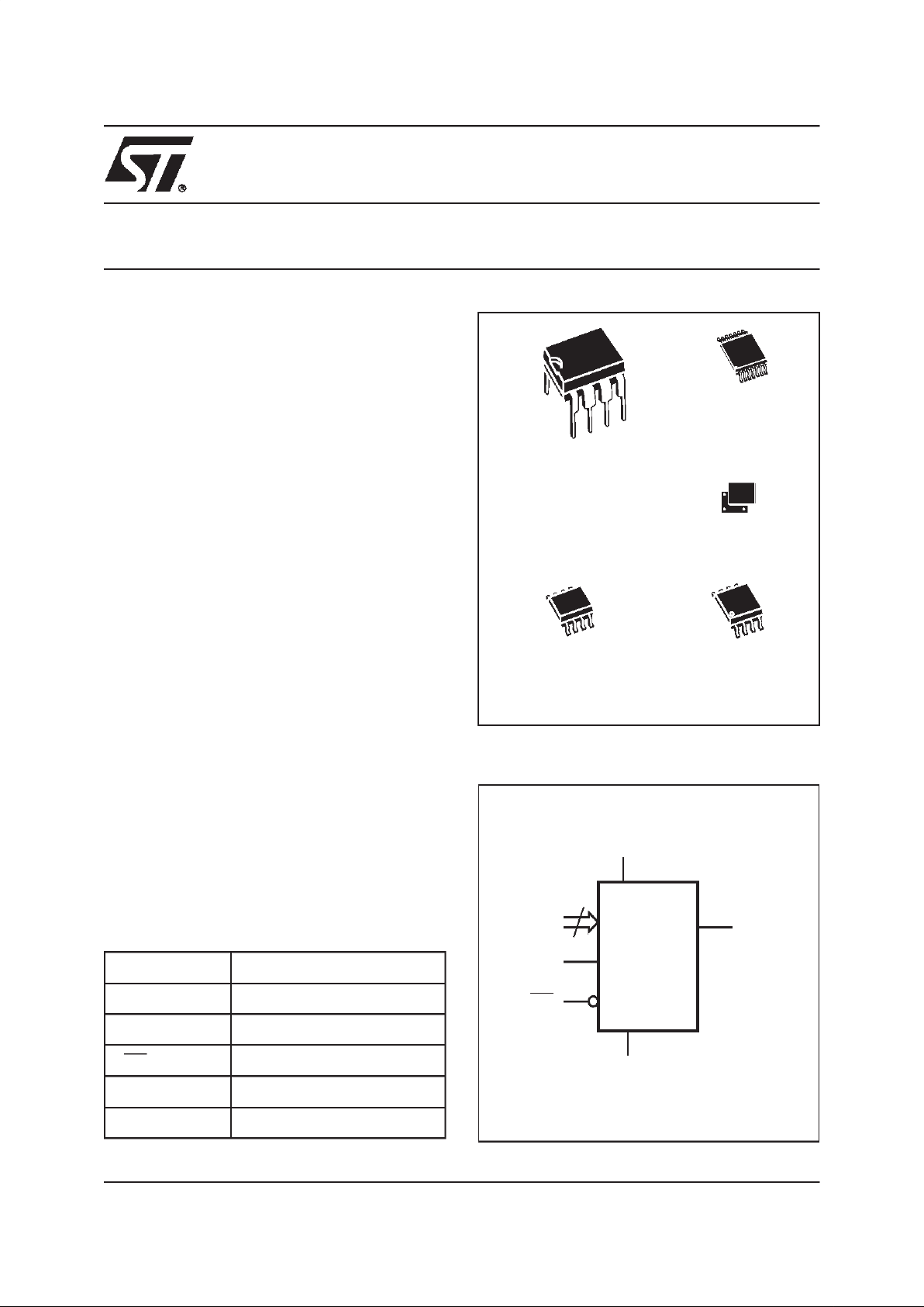
The M24256-A is available in Plastic Dual-in-Line,
Plastic Small Outline and Thin Shrink Small Outline packages. The M24256-A is also available in
a chip-scale (SBGA) package.
Figure 1. Logic Diagram
AI02271C
SDA
V
CC
M24256-A
WC
SCL
V
SS
2
E0-E1
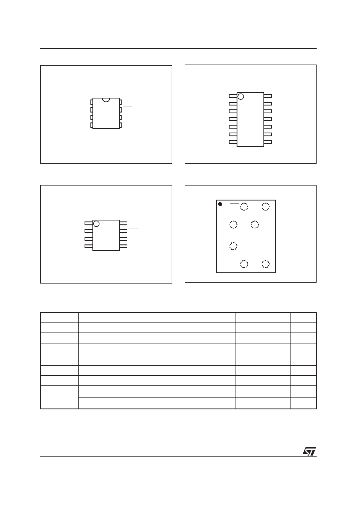
Table 1. Signal Names
E0, E1 Chip Enable
SDA Serial Data
SCL Serial Clock
WC Write Control
V
CC
Supply Voltage
V
SS
Ground
PSDIP8 (BN)
0.25 mm frame
SO8 (MN)
150 mil width
TSSOP14 (DL)
169 mil width
8
1
8
1
14
1
SO8(MW)
200 mil width
8
1
SBGA
SBGA7 (EA)
140 x 90 mil
M24256-A
2/20
Figure 2A. DIP Connections
Note: 1. NC = Not Connected
Figure 2B. SO Connections
Note: 1. NC = Not Connected
SDAV
SS
SCL
WCE1
E0 V
CC
NC
AI02273C
M24256-A
1
2
3
4
8
7
6
5
1
AI02272C
2
3
4
8
7
6
5 SDAV
SS
SCL
WCE1
E0 V
CC
NC
M24256-A
Figure 2C. TSSOP Connections
Note: 1. NC = Not Connected
Figure 2D. SBGA Connections (top view)
1
AI02388C
2
3
4
14
9
10
8 SDAV
SS
NC SCL
E0
WC
M24256-A
NC
E1
NC
NC NC
NC
NC
5
6
7
12
13
11
V
CC
AI03760
SCL
V
SS
SDA
WC
V
CC
M24256-A
S1
S0
Table 2. Absolute Maximum Ratings
1
Note: 1. Except for the rating “Operating Temperature Range”, stresses above those listed in the Table “Absolute Maximum Ratings” may
cause permanent damage tothe device.These are stress ratings only, and operation of thedevice at these or any other conditions
above those indicated in the Operating sections of this specification is not implied. Exposure to Absolute Maximum Rating conditions forextended periods may affect device reliability. Refer also to the ST SURE Program and other relevant quality documents.
2. MIL-STD-883C, 3015.7 (100 pF, 1500 Ω)
3. EIAJ IC-121 (Condition C) (200 pF, 0 Ω)
Symbol Parameter Value Unit
T
A
Ambient Operating Temperature –40 to 125 °C
T
STG
Storage Temperature –65 to 150 °C
T
LEAD
Lead Temperature during Soldering
PSDIP8: 10 sec
SO8: 40 sec
TSSOP14: t.b.c.
260
215
t.b.c.
°C
V
IO
Input or Output range –0.6 to 6.5 V
V
CC
Supply Voltage –0.3 to 6.5 V
V
ESD
Electrostatic Discharge Voltage (Human Body model)
2
4000 V
Electrostatic Discharge Voltage (Machine model)
3
200 V
3/20
M24256-A
These memory devices are compatible with the
I2C extended memory standard. This is a two wire
serial interface that uses a bi-directional data bus
and serial clock. The memory carries a built-in 4bit unique Device Type Identifier code (1010) in
accordance with the I2C bus definition.
The memory behaves as a slave device in the I2C
protocol, with all memory operations synchronized
by the serial clock. Read and Write operations are
initiated by a START condition, generated by the
bus master. The START condition isfollowed by a
Device Select Code and RW bit (as described in
Table 3), terminated by an acknowledge bit.
When writing data to the memory, the memory inserts an acknowledge bit during the 9thbit time,
following the bus master’s 8-bit transmission.
When data is read by the bus master, the bus
master acknowledges the receipt of the data byte
in the same way. Data transfers areterminated by
a STOP condition after an Ack for WRITE, and after a NoAck for READ.
Power On Reset: VCCLock-Out Write Protect
In orderto prevent data corruption and inadvertent
write operations during power up, a Power On Reset (POR) circuit is included. The internal reset is
held active until the VCCvoltage has reached the
POR threshold value, and all operations are disabled – the device will not respond to any command. In the same way,when VCCdrops from the
operating voltage, below thePOR thresholdvalue,
all operations are disabled and the device will not
respond to any command. A stable and valid V
CC
must be applied before applying any logic signal.
SIGNAL DESCRIPTION
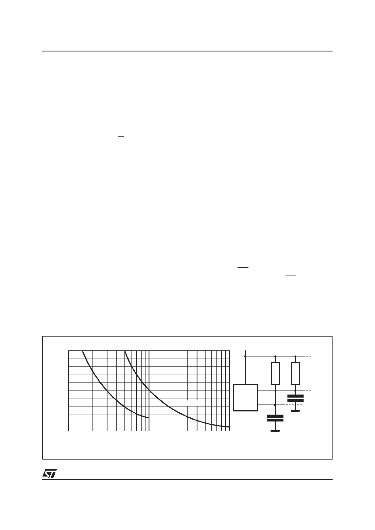
Serial Clock (SCL)
The SCL input pin is used to strobe all data in and
out of the memory. In applications where this line
is usedby slavesto synchronize thebus to aslower clock, the master must have an open drain output, anda pull-up resistormust be connectedfrom
the SCL line to VCC. (Figure 3 indicates how the
value of the pull-up resistor can be calculated). In
most applications, though,this method of synchronization is not employed, and so the pull-up resistor is not necessary, provided that the master has
a push-pull (rather than open drain) output.
Serial Data (SDA)
The SDA pin is bi-directional, and is used to transfer datain or out of the memory. It isan open drain
output that may be wire-OR’ed with other open
drain or open collector signals on the bus. A pull
up resistor must be connected from the SDA bus
to VCC. (Figure 3 indicates how the value of the
pull-up resistor can be calculated).
Chip Enable (E1, E0)
These chip enable inputs are used toset thevalue
that is to be looked for on the two least significant
bits (b2, b1) of the 7-bit device select code. These
inputs must be tied to VCCor VSSto establish the
device select code. When unconnected, the E1
and E0 inputs areinternally read as VIL(see Table
7 and Table 8)
Write Control (WC)
The hardware Write Control pin (WC) is useful for
protecting the entire contents of the memory from
inadvertenterase/write. TheWrite Control signalis
used to enable (WC=VIL) or disable (WC=VIH)
write instructions to the entire memoryarea. When
Figure 3. Maximum RLValue versus Bus Capacitance (C
BUS
) for an I2C Bus
AI01665
V
CC
C
BUS
SDA
R
L
MASTER
R
L
SCL
C
BUS
100
0
4
8
12
16
20
C
BUS
(pF)
Maximum RP value (kΩ)
10 1000
fc = 400kHz
fc =100kHz
M24256-A
4/20
unconnected, the WC input is internally read as
VIL, and write operations are allowed.
When WC=1, Device Select and Address bytes
are acknowledged, Data bytes are not acknowledged.
Please seethe Application Note
AN404
fora more
detailed description of the Write Control feature.
DEVICE OPERATION
The memory device supports the I2C protocol.
This is summarized in Figure 4, and is compared
with other serial bus protocols in Application Note
AN1001
. Any device thatsends data on to the bus
is defined to be a transmitter, and any device that
reads the data to be a receiver. The device that
controls the data transfer is known as the master,
and theother asthe slave.A data transfer canonly
be initiated by the master, which will also provide
the serial clock for synchronization. The memory
device is always a slave device in all communication.
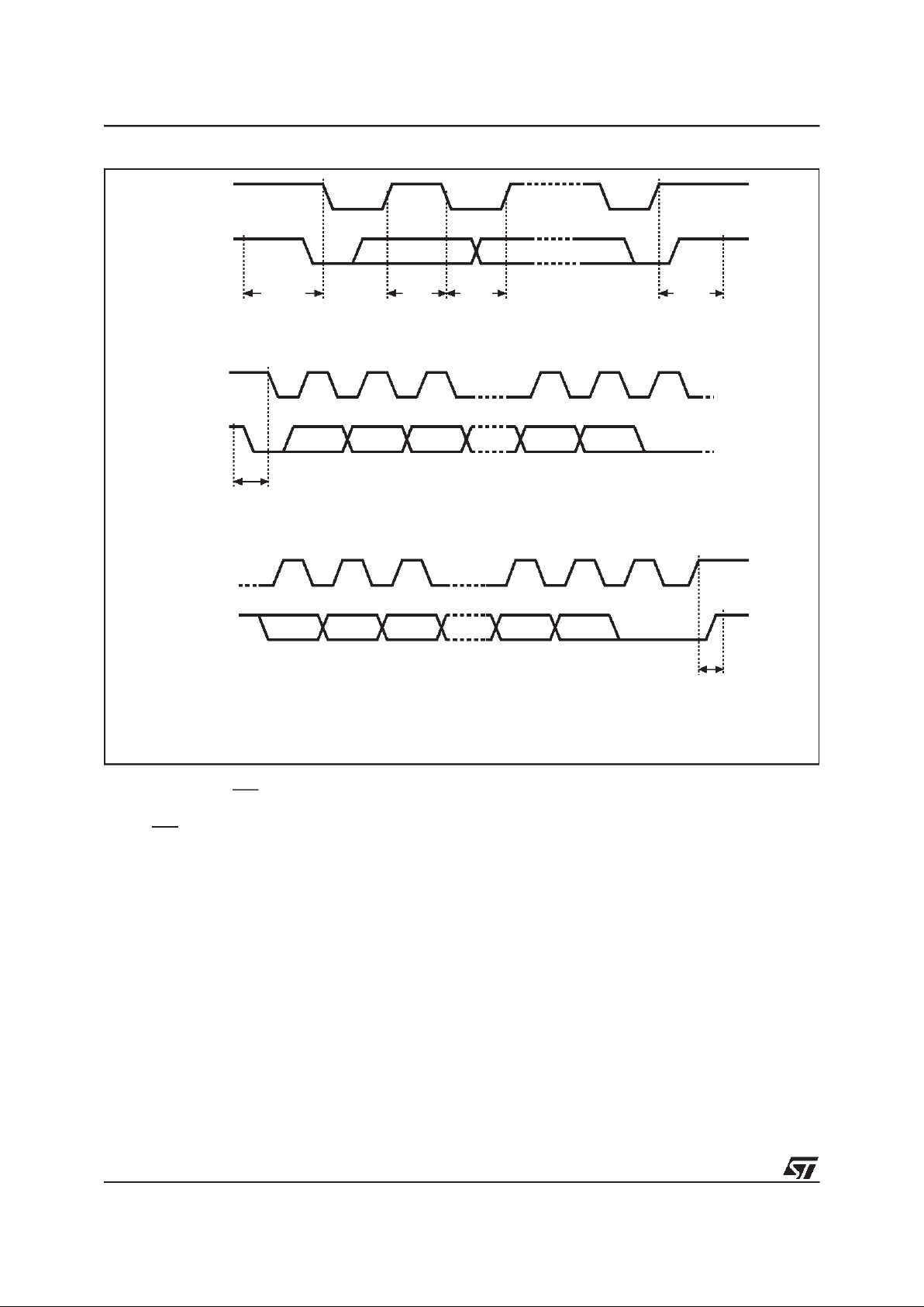
Start Condition
START is identified by a high to low transition of
the SDA line while the clock, SCL, is stable in the
high state. A START condition must precede any
data transfer command. The memory device continuously monitors (except during a programming
cycle) the SDA and SCL lines for a START condition, and will not respond unless one is given.
Stop Condition
STOP isidentified by alow to hightransition of the
SDA line while the clock SCL is stable in the high
state. A STOP condition terminates communication between the memory device and the busmaster. A STOP condition at the end of a Read
command, after (and only after) a NoAck, forces
the memory device into its standby state. A STOP
condition at the end of a Write command triggers
the internal EEPROM write cycle.
Figure 4. I2C Bus Protocol
SCL
SDA
SCL
SDA
SDA
START
CONDITION
SDA
INPUT
SDA
CHANGE
AI00792
STOP
CONDITION
123 789
MSB
ACK
START
CONDITION
SCL
123 789
MSB ACK
STOP
CONDITION
5/20
M24256-A
Acknowledge Bit (ACK)
An acknowledge signal is used to indicate a successful byte transfer. The bus transmitter, whether
it be master or slave, releases the SDA bus after
sending eight bits of data. During the 9thclock
pulse period, the receiver pulls the SDA bus low to
acknowledge the receipt of the eight data bits.
Data Input
During data input, thememory device samplesthe
SDA bus signal on the rising edge of the clock,
SCL. For correct device operation, theSDA signal
must be stable during the clock low-to-high transition, andthe data must change
only
when theSCL
line is low.
Memory Addressing
To start communication between the bus master
and the slave memory, the master must initiate a
START condition.Following this,the master sends
the 8-bit byte, shown in Table 3, on the SDA bus
line (most significant bit first). This consists of the
7-bit DeviceSelect Code, andthe 1-bitRead/Write
Designator (RW). The Device Select Code is further subdivided into:a 4-bit DeviceType Identifier,
and a 3-bit Chip Enable “Address” (0, E1, E0).
To address the memory array, the 4-bit Device
Type Identifier is 1010b.
Up to fourmemory devices can be connected ona
single I2C bus. Each one is given a unique 2-bit
code on its Chip Enable inputs. When the Device
Select Codeis received onthe SDA bus, the memory only responds if the Chip Select Code is the
same as the pattern applied to its Chip Enable
pins.
The 8thbit is the RW bit. This is set to ‘1’ for read
and ‘0’ for write operations. If a match occurs on
the Device Select Code, the corresponding memorygives anacknowledgment onthe SDAbus during the 9thbit time. If the memory does not match
the DeviceSelect Code, itdeselects itself from the
bus, and goes into stand-by mode.
There are two modes both for read and write.
These are summarized in Table 6 and described
later. A communication between the master and
the slave is ended with a STOP condition.
Each data byte in the memory has a 16-bit (two
bytewide) address. The MostSignificantByte (Table 4) is sent first, followed by theLeast significant
Byte (Table 5). Bits b15 to b0 form theaddress of
the byte in memory. Bit b15 is treated as Don’t
Care bits on the M24256-A memory.
Write Operations
Following a START condition the master sends a
Device Select Code with the RW bit set to ’0’, as
shown in Table 6.Thememory acknowledges this,
and waits for two address bytes. The memory re-
Table 3. Device Select Code
1
Note: 1. The most significant bit, b7, is sent first.
Device Type Identifier Chip Enable RW
b7 b6 b5 b4 b3 b2 b1 b0
Device Select Code 1 0 1 0 0 E1 E0 RW
Table 4. Most Significant Byte
Note: 1. b15 is treated as Don’t Care on the M24256-A series.
Table 5. Least Significant Byte
b15 b14 b13 b12 b11 b10 b9 b8
b7 b6 b5 b4 b3 b2 b1 b0
Table 6. Operating Modes
Note: 1. X = V
IH
or V
IL
.
Mode RW bit
WC
1
Data Bytes Initial Sequence
Current Address Read 1 X 1 START, Device Select, RW = 1
Random Address Read
0X
1
START, Device Select, RW = 0, Address
1 X reSTART, Device Select, RW = 1
Sequential Read 1 X ≥ 1 Similar to Current or Random Address Read
Byte Write 0 V
IL
1 START, Device Select, RW = 0
Page Write 0 V
IL
≤ 64 START, Device Select, RW = 0
M24256-A
6/20
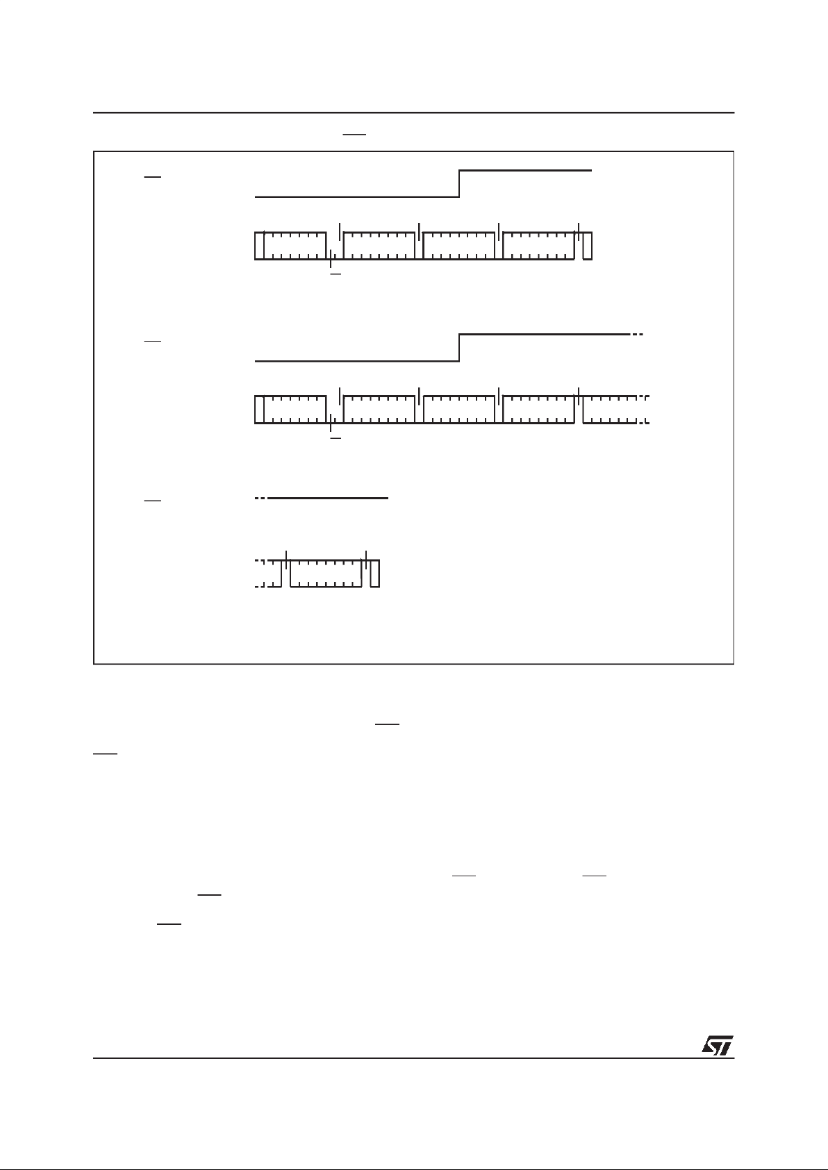
Figure 5. Write Mode Sequences with WC=1 (data write inhibited)
STOP
START
BYTE WRITE DEV SEL BYTE ADDR BYTE ADDR DATA IN
WC
START
PAGE WRITE DEV SEL BYTE ADDR BYTE ADDR DATA IN 1
WC
DATA IN 2
AI01120B
PAGE WRITE
(cont’d)
WC (cont’d)
STOP
DATA IN N
ACK ACK ACK NO ACK
R/W
ACK ACK ACK NO ACK
R/W
NO ACK NO ACK
sponds toeach address byte withan acknowledge
bit, and then waits for the data byte.
Writing to the memory may be inhibited if the WC
input pin is taken high. Any write command with
WC=1 (during a period of time from the START
condition until the end of the two address bytes)
will not modify the memory contents, and the accompanying data bytes will
not
be acknowledged,
as shown in Figure 5.
Byte Write
In the Byte Write mode, after the Device Select
Code and the address bytes, the master sends
one data byte. If the addressed location is write
protected by the WC pin, the memory replies with
a NoAck, and the location is not modified. If, instead, the WC pin has been held at 0, as shown in
Figure 6, the memory replies with an Ack. The
master terminates the transfer by generating a
STOP condition.
Page Write
The Page Write mode allows up to 64 bytes to be
written in a single write cycle, provided that they
are all located in the same ’row’ in the memory:
that is the most significant memory address bits
(b14-b6 for the M24256-A) are the same. If more
bytes are sentthan will fit up to the endof the row,
a conditionknown as ‘roll-over’ occurs.Data starts
to becomeoverwritten (in a way notformally specified in this data sheet).
The master sends from one up to64 bytes of data,
each of which is acknowledged by the memory if
the WC pin is low. If the WC pin is high, the contents of the addressed memory location are not
modified, and each data byte is followed by a
NoAck. After each byte is transferred, theinternal
byte address counter (the 6 least significant bits
only) is incremented. The transferis terminated by
the master generating a STOP condition.
When the master generates a STOP condition immediately after the Ack bit (in the “10thbit” time
 Loading...