

SGS Thomson Microelectronics M24164 Datasheet
TWO WIRE I2C SERIAL INTERFACE
SUPPORTS 400kHz PROTOCOL
1 MILLION ERASE/WRITE CYCLES
40 YEARS DA TA RETE NT ION
2ms TYPICAL PROGRAMMING TIME
SINGLE SUPPLY VOLTAGE:
– 4.5V to 5.5V for M24164
– 2.5V to 5.5V for M24164-W
– 1.8V to 5.5V for M24164-R
HARDWARE WRITE CONT ROL
BYTE and PAGE WRITE (up to 16 BYTES)
BYTE, RANDOM and SEQUENTIAL READ
MODES
SELF TIMED PROGRAMMING CYCLE
AUTOMATIC ADDRESS INCREMENTING
ENHANCED ESD/LA T CH-UP
PERFORMANCES
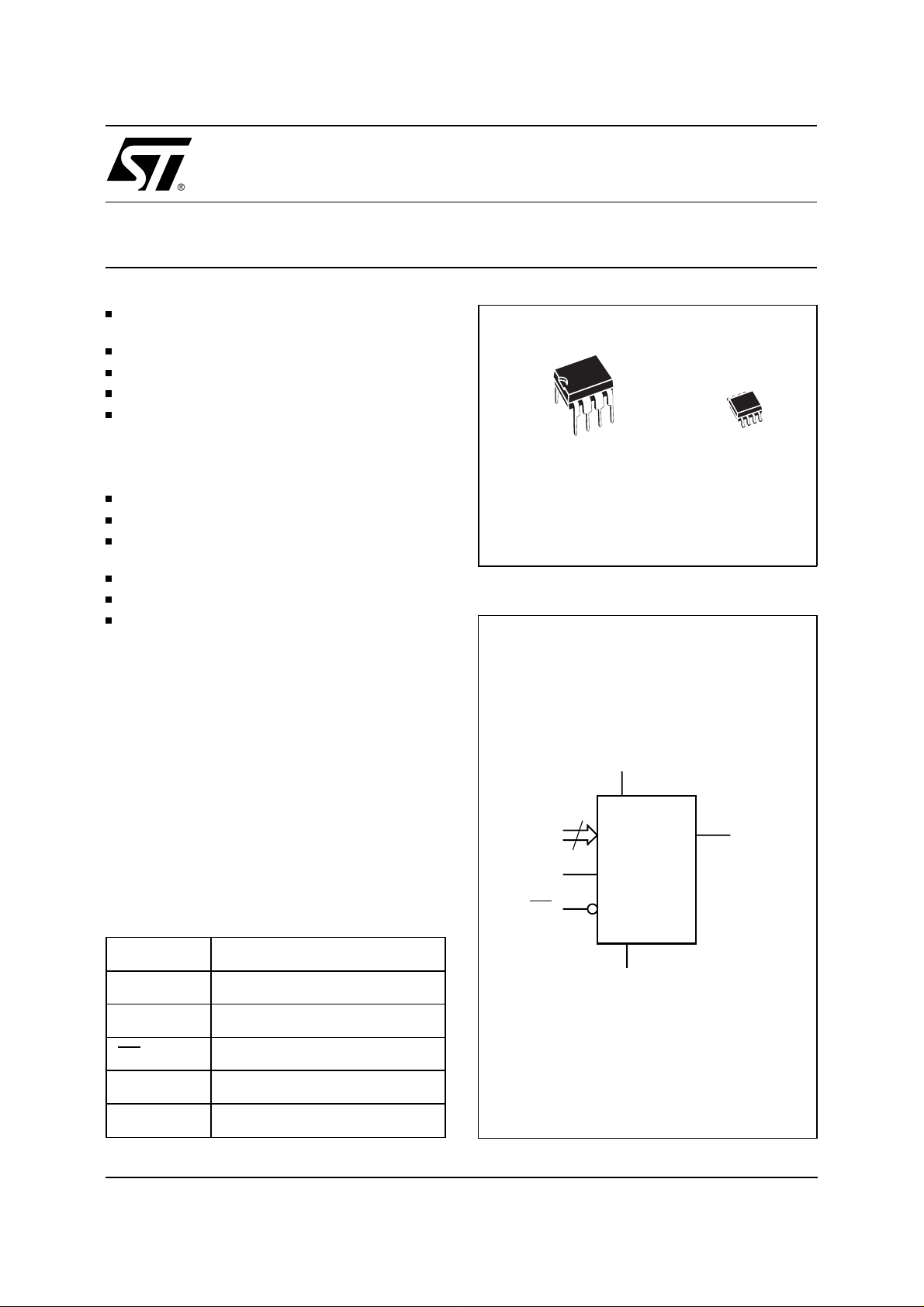
M24164
16 Kbit Serial I2C BUS EEPROM
PRELIMINARY DATA
8
1
PSDIP8 (BN)
0.25mm Frame
Figure 1. Logic Diagram
8
1
SO8 (MN)
150mil Width
DESCRIPTION
The M24164 is a 16 Kbit EEPROM. The memory
is an electrically erasable programmable memory
(EEPROM) fabricated with STMicroelectronics’s
High Endurance Single Polysilicon CMOS technology which guarantees an endurance typically well
above one million erase/write cycles with a data
retention of 40 years. The "-W" version operate with
a power supply value as low as 2.5V and the "-R"
version operate down to 1.8V.
Both Plastic Dual-in-Line and Plastic Small Out line
packages are available.
T ab le 1. Signal Names
E0-E2 Chip Enable Inputs
SDA Serial Data Address Input/Output
SCL Serial Clock
WC Write Control
V
CC
V
SS
Supply Voltage
Ground
V
CC
3
E0-E2 SDA
SCL
WC
M24164
V
SS
AI02264
January 1999 1/16
This is preliminary information on a new product now in development or undergoing evaluation. Details are subject to change without noti ce.
M24164
T ab le 2. Absolute Maximum Ratings
Symbol Parameter Value Unit
T
T
V
Notes:
T
STG
LEAD
V
V
ESD
Ambient OperatingTemperature
A
Storage Temperature –65 to 150
Lead Temperature, Soldering (PSDIP8 package) 10 sec
Input or Output Voltages –0.6 to 6.5 V
IO
Supply Voltage –0.3 to 6.5 V
CC
Electrostatic Discharge Voltage (Human Body model)
Electrostatic Discharge Voltage (Machine model)
1. Except for the rating "Operating Temperature Range", stresses above those listed in the Table "Absolute Maximum Ratings"
may cause permanent damage to the device. These are stress rating s only and operation of the device at these or any other
conditions above those indicated in the Operating sections of this specification is not implied. Exposure to Absolute Maximum
Rating conditions for extended periods may affect device reliability. Refer also to the STMicroelectronics SURE Program and other
relevant quality documents.
2. Depends on range.
3. MIL-STD-883C, 3015.7 (100pF, 1500 Ω).
4. EIAJ IC-121 (Condition C) (200pF, 0 Ω).
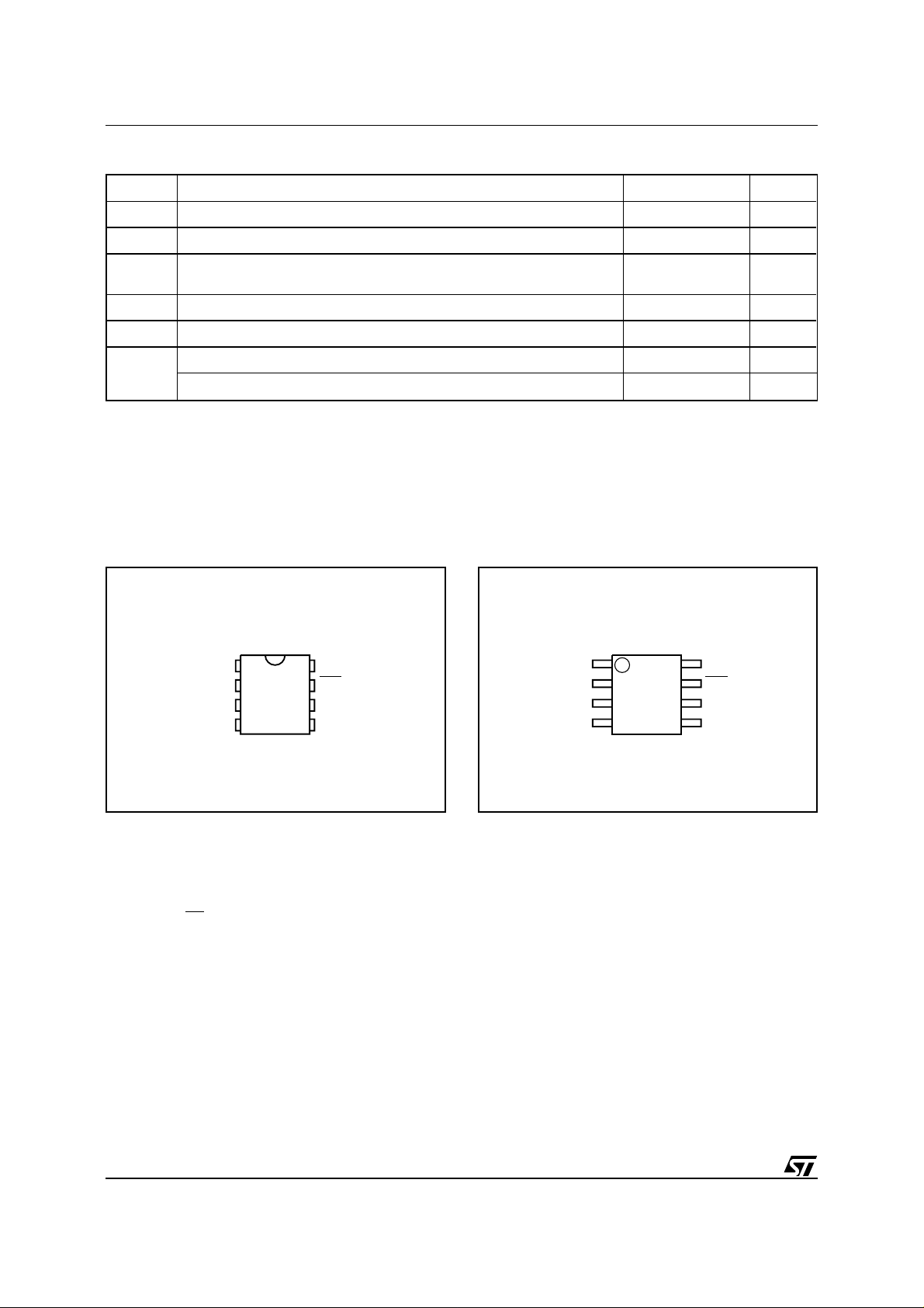
Figure 2A. DIP Pin Connections
(1)
(2)
(SO8 package) 40 sec
(3)
(4)
Figure 2B. SO Pin Connections
–40 to 125
260
215
4000 V
500 V
C
°
C
°
C
°
M24164
1
E0 V
2
3
E2
4
SS
8
7
6
5
AI02265
CC
WCE1
SCL
SDAV
DESCRIPTION (cont’d)
The memory is compatible with the two wire serial
interface which uses a bi-directional data bus and
serial clock. The memory offers 3 chip enable
inputs (E2,
E1, E0) so that up to 8 x 16K devices
may be attached to the bus and selected individually. The memory behaves as a slave device with
all memory operations synchronized by the serial
clock.
Read and write operations are initiated by a ST ART
condition generated by the bus master. The ST ART
condition is followed by a s tream of 7 bit s, plus one
read/write bit and terminated by an acknowledge
bit (see T able 3). When writing data to the memory
it responds to the 8 bits received by assertin g an
acknowledge bit during the 9th bit time. When data
M24164
1
E0 V
2
3
E2
SS
4
8
7
6
5
AI02266
CC
WCE1
SCL
SDAV
is read by the bus master, it acknowledges the
receipt of the data bytes in t he same way. Data
transfers are terminated with a STOP condition.
Power On Reset: V
lock out write protect . In
CC
order to prevent any possible data corruption and
inadvertent write operations during power up, a
Power On Reset (POR) circuit is implemented.
Until the V
voltage has reached the P OR thresh-
CC
old value, the internal reset is active, all operations
are disabled and the device will not respond t o any
command. In the same way , when V
drops down
CC
from the operating voltage to below the POR
threshold value, all operations are disabled and the
device will not respond to any command. A stable
V
must be applied before applying any logic
CC
signal.
2/16
M24164
T ab le 3. Device Select Code
Chip Enable MSB Address RW
Bit b7 b6 b5 b4 b3 b2 b1 b0
Device Select 1 E2
Note:
The MSB b7 is sent first.
T ab le 4. Operating Modes
Mode RW bit WP Data Bytes Initial Sequence
Current Address Read ’1’ X 1 STAR T, Device Select, R
Random Address Read
Sequential Read ’1’ X
Byte Write ’0’ V
Page Write ’0’ V
Note:
1. X = V
or VIL.
IH
(1)
’0’ X
’1’ X reSTART, Device Select, R
SIGNAL DESCRIPTIONS
Serial Clock (SCL). The SCL input pin is used to
synchronize all data in and out of the memory. A
resistor can be connected from the SCL line to V
to act as a pull up (see Figure 3).
Serial Data (SDA). The SDA pin is bi-directional
and is used to transfer data in or out of the memory.
It is an open drain output that may be wire-OR’ ed
with other open drain or open collector signals on
the bus. A resistor must be connected from the SDA
bus line to V
to act as pull up (see Figure 3).
CC
Chip Enable (E2 - E 0). These chip enable inpu ts
are used to set 3 bits (b6, b5, b4) of the 7 bit device
select code. These inputs may be driven dynamically or tied to V
or VSS to establish the device
CC
select code.
Write Control (
(
WC) is provided on pin 7 of the memory. This
WC). A hardware Write Control pin
feature is useful to protect the entire contents of the
memory from any erroneous erase/write cycle. The
Write Control signal is used to enable (
disable (
WC=VIH) write instructions to the entire
memory area. When unconnected, the
internally read as V
allowed. When
WC=1, Device Select and Address
and write operations are
IL
bytes are acknowledged, Data by tes are not acknowledged.
Refer to Application Note AN404 for more detailed
E1 E0 A10 A9 A8 RW
1
1 As CURRENT or RANDOM Mode
≥
1 START, Device Select, RW = ’0’
IL
IL
16 START, Device Select, RW = ’0’
≤
START, Device Select, R
DEVICE OPERATION
2
I
CC
C Bus Background
The memory supports the I
col defines any device that sends data onto the bus
2
C protocol. This proto-
as a transmitter and any device that reads the data
as a receiver. The device that controls the data
transfer is known as the master and t he other as
the slave. The master will always initiate a data
transfer and will provide the serial clock for synchronisation. The memory is always a slave device
in all communications.
Start Condition. START is identified by a high to
low transition of the SDA line while the clock SCL
is stable in the high state. A ST AR T condition must
precede any command for data transfer. Except
during a programming cycle, the memory continuously monitors the SDA and SCL signals for a
START condition and will not r espond unless one
is given.
Stop Condition. STOP is identified by a low to high
WC=VIL) or
WC input is
transition of the SDA line while the clock SCL is
stable in the high s tate. A STOP condition terminates communication between the memory and the
bus master . A S TOP condition at the end of a Read
sequence, after and only after a No-Ac knowledge,
forces the standby state. A STOP condition at the
end of a Write command triggers the internal
EEPROM write cycle.
information about Write Control feature.
W = ’1’
W = ’0’, Address,
W = ’1’
3/16
M24164
Acknowledge B it ( ACK). An acknowledge signal
is used to indicate a suc cessful data transfer. The
bus transmitter, eit her master or s lave, will release
the SDA bus after sending 8 bits of data. During the
9th clock pulse period the receiver pulls t he SDA
bus low to acknowledge the receipt of the 8 bits of
data.
Data Input. During data input the memory samples
the SDA bus signal on the rising edge of the clock
SCL. Note that for correct device operation, the
SDA s ignal must be stable during the clock low to
high transition and the data must change ONLY
when the SCL line is low.
Memory Addressing. To start communication between the bus master and the slave memory, the
master must initiate a START condition. Following
this, the master sends onto the SDA bus line 8 bits
(MSB first) corresponding to the Device Select
code (7 bits) and a READ or WRITE bit.
Three out of the four most significant bits of the
Device Select code are the Device Select bits (b6,
b5, b4). They are matched to the chip enable
signals applied on pins E2,
E1, E0 . T h us up to 8 x
16K memories can be connected on the same bus
giving a memory capacity total of 128 Kbits.
After a START condition any memory on the bus
will identify the device code and compare the 3 bits
to its chip enable inputs E2,
is the read or write bit (R
E1, E0. The 8th bit sent
W).
This bit is set to ’1’ for read and ’0’ for write
operations. If a match is found, the corresponding
memory will acknowledge the identification on the
SDA bus during the 9th bit time. If the memory does
not match the Device Select code, it will self-deselect from the bus and go into standby mode.
Write Operations
Following a START condition the master sends a
Device Select code with the R
W bit set to ’0’. The
memory acknowledges it and waits for a byte address, which provides access t o the m emory area.
After receipt of the byte address, the memory again
responds with an acknowledge and waits for the
data byte. Writing in the Memory may be inhibited
if input pin
Any write command with
WC is taken high.
WC=1 (during a period of
time from the START condition until the Acknowledge of the last Data byte) will not modify the
memory content and will NOT be acknowledged on
data bytes, as shown in Figure 9.
Byte Write. In the Byte Write mode, after the
Device Select code and the address, the master
sends one data byte. If the addressed location is
write protected by the
NoACK and the location is not modified. If the
WC pin, the memory send a
WC
pin is tied to 0, after the data byte the memory
sends an ACK. The master terminates the transfer
by generating a STOP condition.
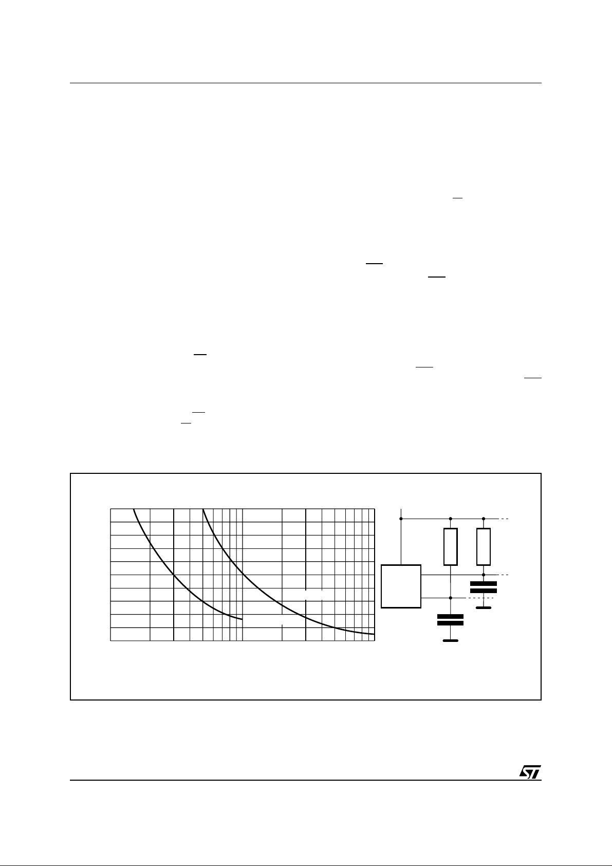
Figure 3. Maximum RL Value versus Bus Capacitance (C
20
16
12
8
Maximum RP value (kΩ)
4
0
10 1000
C
BUS
fc = 400kHz
100
(pF)
fc = 100kHz
) for an I2C Bus
BUS
V
MASTER
CC
SDA
SCL
R
R
C
BUS
L
C
BUS
AI01665
L
4/16
M24164
T able 5. Input Parameters
(1)
(TA = 25°C, f = 400 kHz )
Symbol Parameter Test Condition Min Max Unit
C
IN
C
IN
t
LP
Note:
1. Sampled only, not 100% tested.
Input Capacitance (SDA) 8 pF
Input Capacitance (other pins) 6 pF
Low-pass filter input time constant
(SDA and SCL)
200 500 ns
T ab le 6. DC Characteristics
(T
= 0 to 70°C or –40 to 85°C; VCC = 4.5V to 5.5V, 2.5V to 5.5V or 1.8V to 5.5V)
A
Symbol Parameter Test Condition Min Max Unit
I
I
I
V
V
V
I
LI
I
LO
I
CC
CC1
CC2
CC3
V
V
OL
Input Leakage Current
(SCL, SDA)
Output Leakage Current
Supply Current
Supply Current (-W series)
Supply Current (-R series)
Supply Current, Standby
Supply Current, Standby
(-W series)
Supply Current, Standby
(-R series)
IL
IH
IL
IH
Input Low Voltage (SCL, SDA,
E2, E1, E0)
Input High Voltage (SCL, SDA,
E2, E1, E0)
Input Low Voltage (WC) –0.3 0.5 V
Input High Voltage (WC) VCC – 0.5 VCC + 1 V
Output Low Voltage IOL = 3mA, VCC = 5V 0.4 V
Output Low Voltage (-W series) I
Output Low Voltage (-R series) I
0V ≤ V
0V ≤ V
V
= 5V, fC = 400kHz
CC
(Rise/Fall time < 30ns)
= 2.5V, fC = 400kHz
V
CC
(Rise/Fall time < 30ns)
= 1.8V, fC = 100kHz
V
CC
(Rise/Fall time < 30ns)
V
IN
VIN = VSS or VCC,
VIN = VSS or VCC,
= 2.1mA, VCC = 2.5V 0.4 V
OL
= 0.15mA, VCC = 1.8V 0.2 V
OL
≤ V
IN
CC
≤ VCC
OUT
SDA in Hi-Z
= VSS or VCC,
V
= 5V
CC
V
= 2.5V
CC
= 1.8V
V
CC
–0.3 0.3 V
0.7 V
CC
VCC + 1 V
2
±
2
±
2mA
1mA
0.8 mA
20
1
0.1
CC
A
µ
A
µ
A
µ
A
µ
A
µ
V
5/16
 Loading...