

SGS Thomson Microelectronics LS204I, LS204C Datasheet
.
LOW POWERCONSUMPTION
.
SHORT CIRCUIT PROTECTION
.
LOW DISTORTION,LOW NOISE
.
HIGHGAIN-BANDWIDTH PRODUCT
.
HIGHCHANNEL SEPARATION
LS204
HIGH PERFORMANCE
DUALOPERATIONAL AMPLIFIERS
DESCRIPTION
The LS204is a highperformance dual operational
amplifier with frequency and phase compensation
builtintothechip.Theinternalphasecompensation
allows stable operation as voltagefollowerin spite
of itshigh Gain-BandwidthProduct.
The circuit presents very stable electrical characteristics over the entire supply voltage range, and
is particularlyintendedforprofessionalandtelecom
applications(activefilter, etc).
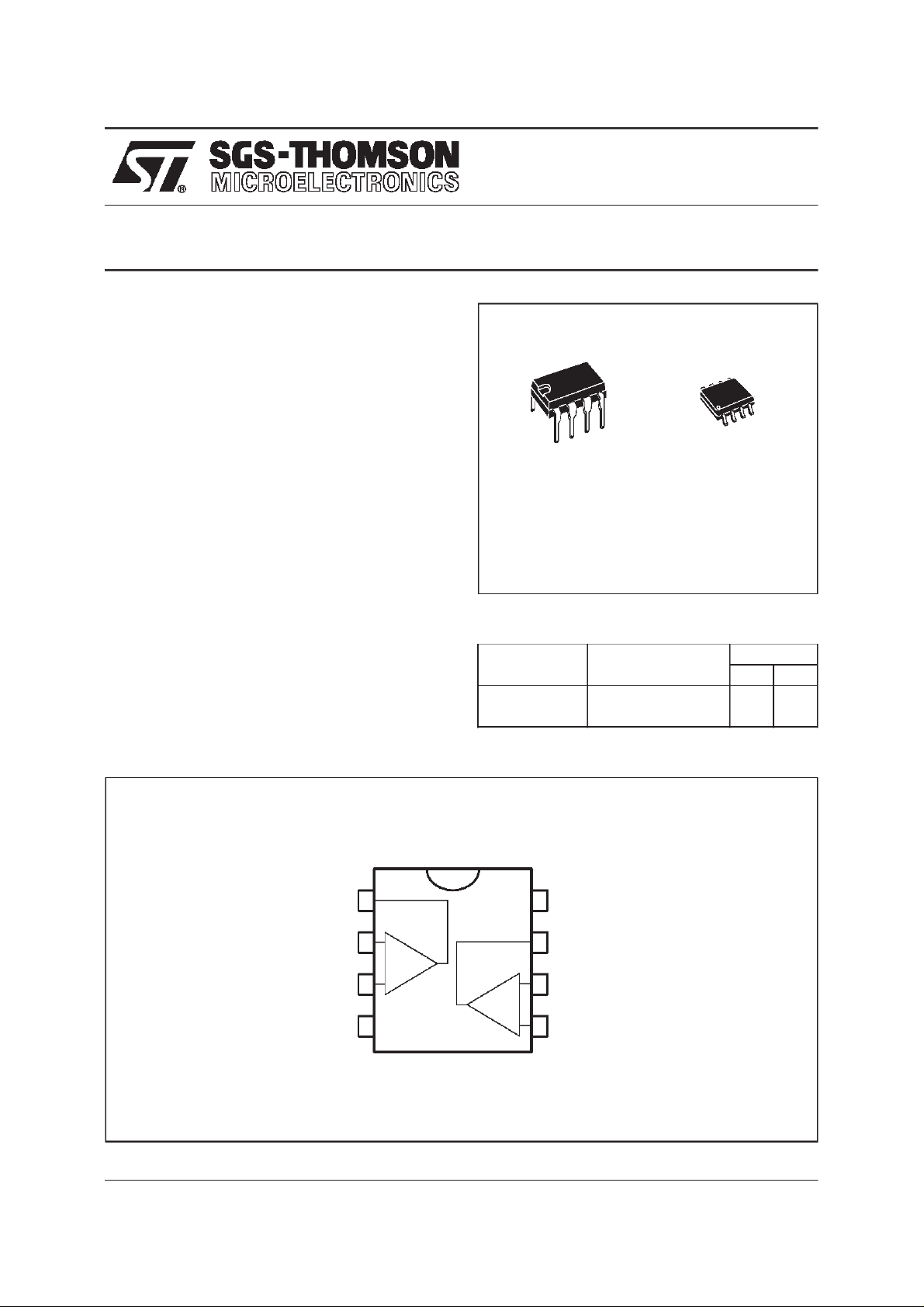
PINCONNECTIONS (top view)
Output 1
1
N
DIP8
(Plastic Package)
ORDER CODES
Part Number Temperature Range
LS204C 0, +70
LS204I -40, +105
8
V
CC
(Plastic Micropackage)
o
C ••
o
+
D
SO8
Package
ND
C ••
April 1998
Inverting Input 1
Non-inverting Input 1
CCV
Output
2
3
-
4
-
+
-
+
7
Non-inverting Input 2
6
Inverting Input 2
5
1/10
LS204
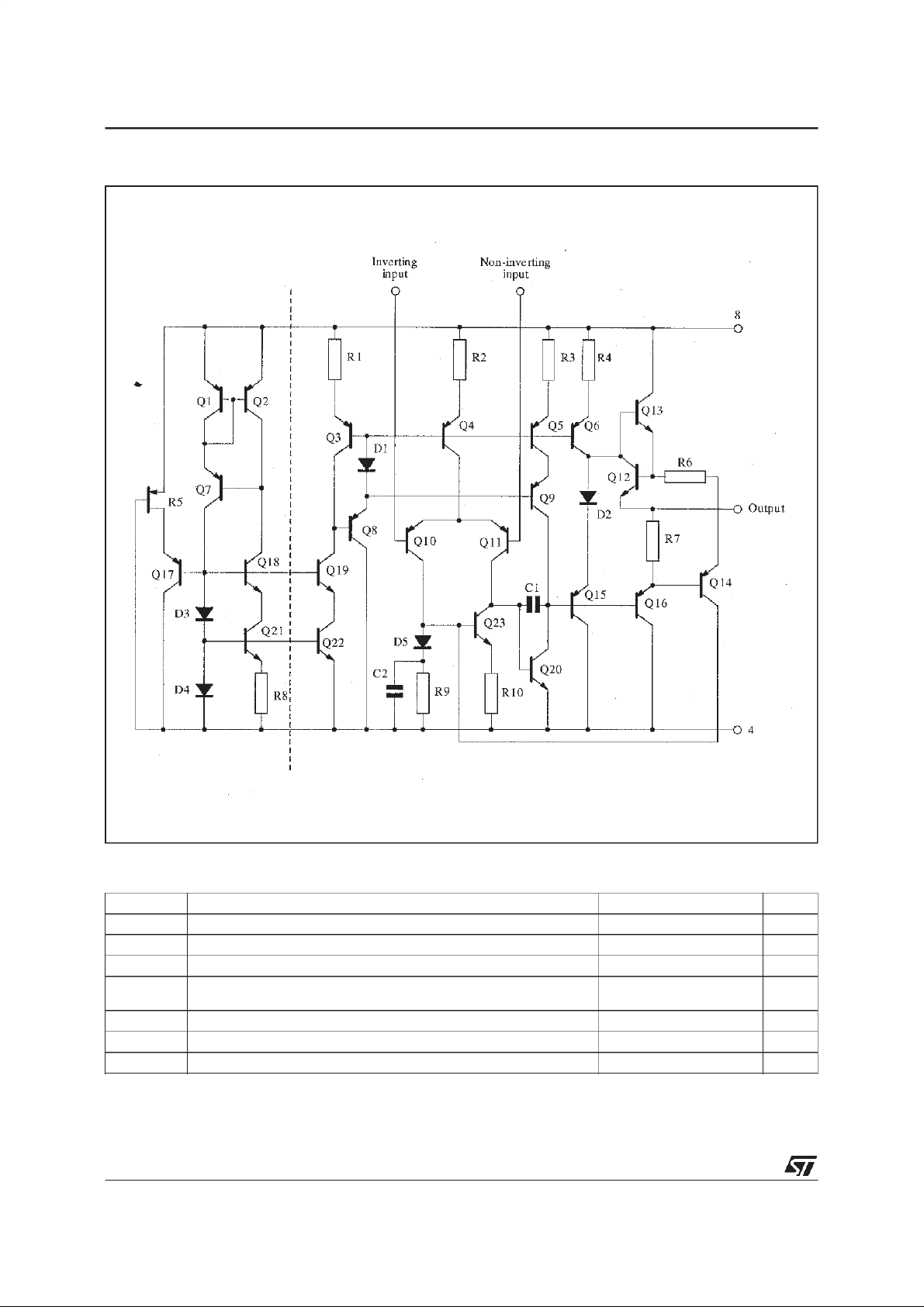
SCHEMATIC DIAGRAM (1/2 LS204)
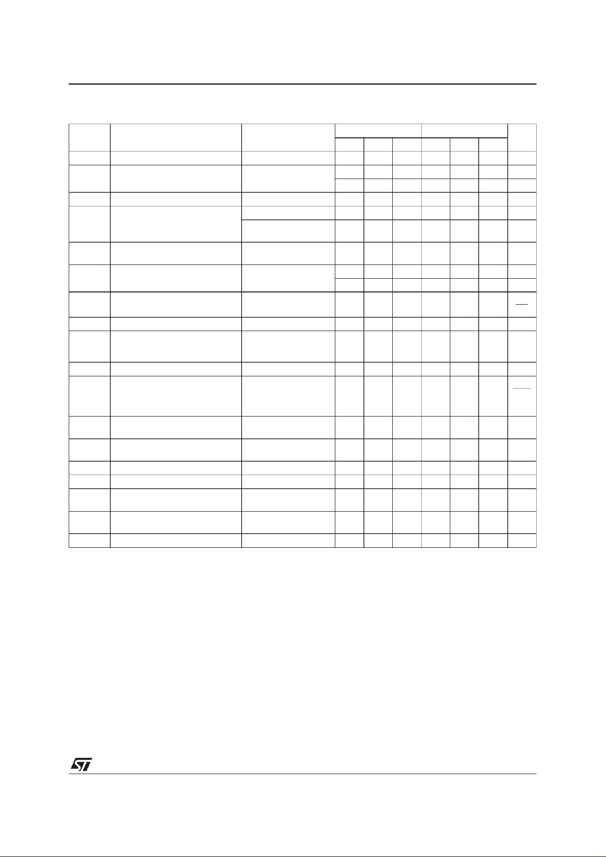
ABSOLUTEMAXIMUM RATINGS
Symbol Parameter Value Unit
SupplyVoltage ±18 V
InputVoltage ±V
i
Differential Input Voltage ± (VCC-1)
id
Operating Temperature Range LS204C
LS204I
Power Dissipation at T
JunctionTemperature 150
j
=70oC 500 mW
amb
CC
0 to +70
-40 to +105
Storage Temperature Range -65 to +150
2/10
V
CC
V
V
T
oper
P
tot
T
T
stg
o
C
o
C
o
C
LS204
ELECTRICALCHARACTERISTICS (VCC= ±15V,T
Symbol Parameter Test Conditions
Supply Current 0.7 1.2 0.8 1.5 mA
I
CC
Input Bias Current 50 150 100 300 nA
I
ib
T
min.<Top<Tmax
Input Resistance f = 1kHz 1 1 MΩ
R
i
Input Offset Voltage Rs≤ 10kΩ 0.5 2.5 0.5 3.5 mV
V
io
≤ 10kΩ
R
s
.<Top<T
T
min
DV
DI
Input Offset VoltageDrift Rs≤ 10kΩ
io
I
Input OffsetCurrent 5 20 12 50 nA
io
Input OffsetCurrent Drift T
io
Output Short Circuit Current 23 23 mA
I
os
Large Signal Voltage Gain T
A
vd
.<Top<T
T
min
.<Top<T
T
min
.<Top<T
min
.<Top<T
min
=2kΩ VCC= ±15V
R
L
V
= 25oC, unless otherwisespecified)
amb
LS204I LS204C
Min. Typ. Max. Min. Typ. Max.
. 300 700 nA
. 3.5 5
max
.2 2
max
. 40 100 nA
max
. 0.08 0.1 nA
max
.
CC
max
= ±4V
90 100
95
86 100
95
GBP Gain-Bandwidth Product f = 100kHz 1.8 3 1.5 2.5 MHz
Equivalent Input Noise Voltage f = 1kHz
e
n
THD Total Harmonic Distortion A
±V
V
Output Voltage Swing RL=2kΩ VCC= ±15V
opp
Large Signal Voltage Swing RL= 10kΩ f = 10kHz 28 28 V
opp
=50Ω
R
s
=1kΩ
R
s
= 10kΩ
R
s
= 20dB RL=2kΩ
V
=2VPPf = 1kHz
V
O
V
CC
= ±4V
8
15 10
10
18
12
20
0.03 0.1 0.03 0.1 %
±13
±3
±13
±3
SR Slew Rate Unity Gain, RL=2kΩ 0.8 1.5 1 V/µs
CMR Common Mode Rejection Ratio V
SVR Supply Voltage Rejection Ratio V
V
O1/VO2
Channel Separation f = 1kHz 100 120 120 dB
= 10V
ic
.<Top<T
T
min
= 1V f = 100Hz
ic
.<Top<T
T
min
.90 86
max
.90 86
max
Unit
mV
µV/
√Hz
°C
dB
nV
V
dB
dB
PP
o
C
3/10
 Loading...