

Memory TAG IC 512 bit High Endurance EEPROM
13.56MHz, ISO 15693 Standard Compliant with E.A.S.
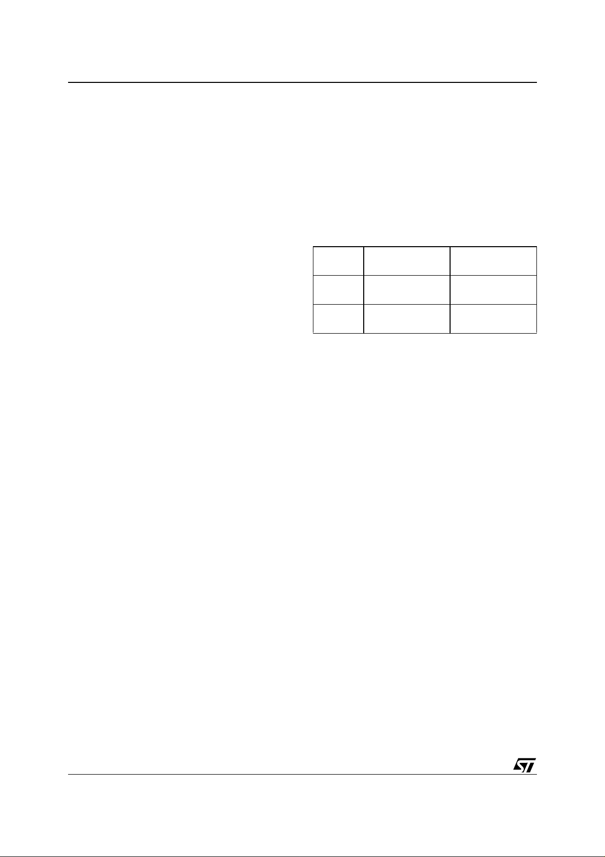
FEATURES SUMMARY
■ ISO15693 Standard: Fully Compliant
■ 13.56 MHz ±7 kHz Carrier Frequency
■ To the LRI512:
10% or 100% ASK modulation using:
– 1/4 pulse position coding (26 kbit/s)
– 1/256 pulse position coding (1.6 kbit/s)
■ From the LRI512:
Load modulation using Manchester coding with
423 kHz and 484 kHz subcarrier in:
– Fast data rate (26 kbit/s)
– Low data rate (6.6 kbit/s)
■ Internal Tuning Capacitor
■ 512 bits EEPROM with Block Lock Featu r e
■ 64-bit Unique Identifier (UID)
■ EAS features
■ READ block and WRITE block (32-bit blocks)
■ 5 ms Programming Time (typical)
■ More than 100,000 Erase/Write Cycles
■ More than 40 Year Data Retention
LRI512
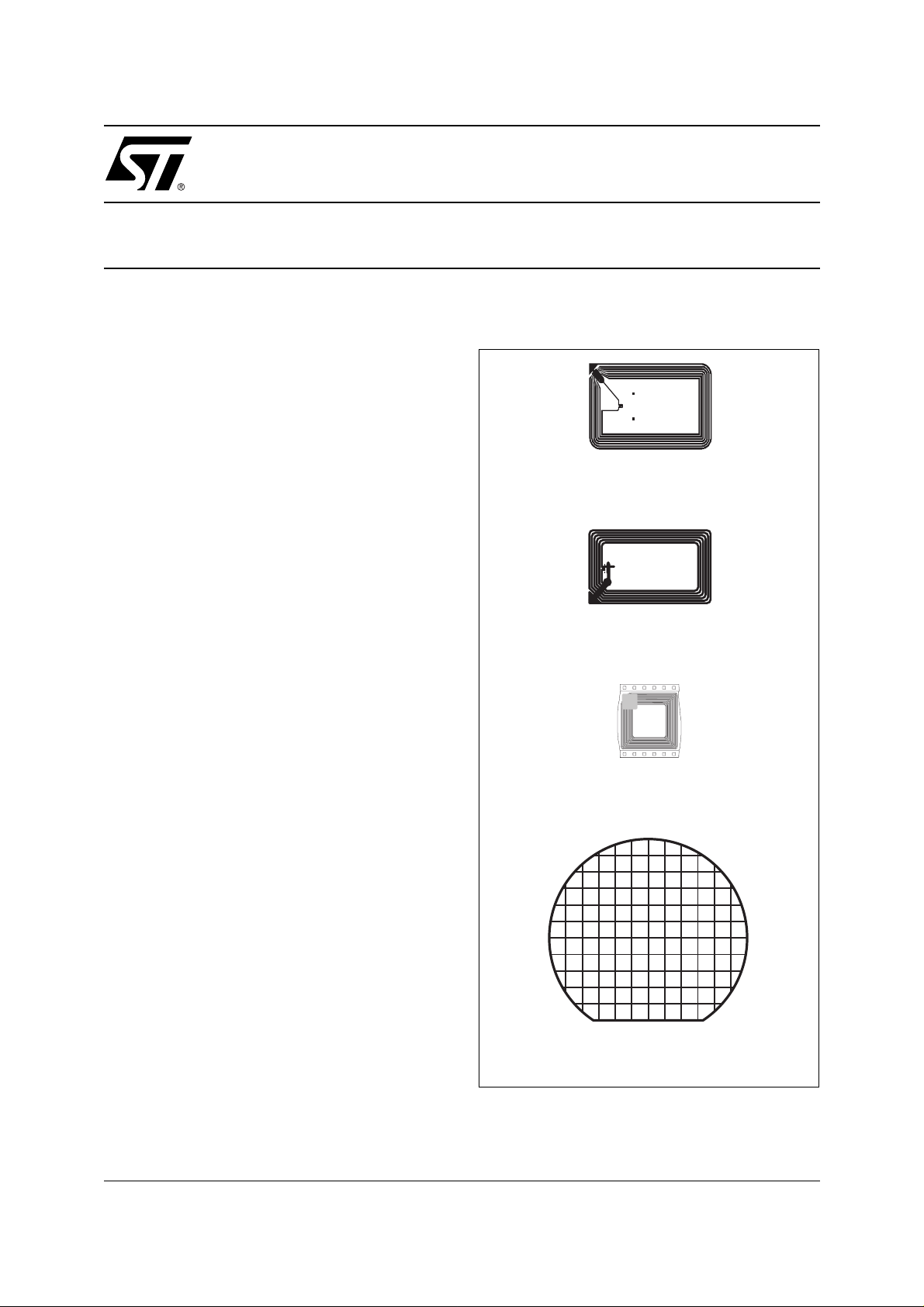
Figure 1. Delivery Forms
Antenna
(A1T/ISOR, A1S/I SOR)
Antenna
(A2T/ISOK)
Antenna
(C40)
Wafer
1/54July 2002
LRI512
SUMMARY DESCRIPTION
The LRI512 is a contactless memory, powered by
an externally transmitted radio wave. It is fully
compliant with the ISO15693 recomm enda tion for
radio-frequency power and signal interface.
The LRI512 contains 512 bits of Electrically
Erasa ble Prog rammabl e Memory (EEPRO M). The
memory is organized as 16 blocks of 32 bits.
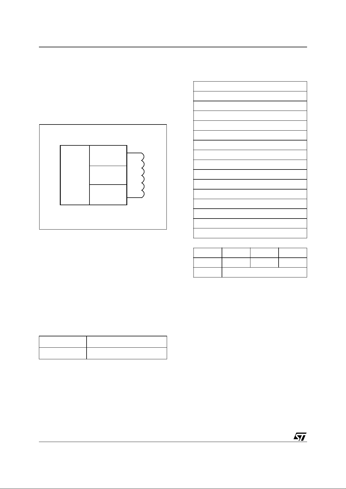
Figure 2. Logic Diagram
LRI512
AC1
AC0
512 bit
EEPROM
Power
Supply
Regulator
ASK
Demodulator
Manchester
Load
Modulator
Table 2. LRI512 Memory Map
Addr 0 7 8 15 16 23 24 31
0 User Area
1 User Area
2 User Area
3 User Area
4 User Area
5 User Area
6 User Area
7 User Area
8 User Area
9 User Area
10 User Area
11 User Area
12 User Area
13 User Area
AI04008B
The LRI512 is accessed by modulating the
13.56 MHz carrier frequency. Incoming data are
demodulated from the received signal amplitude
modulation (ASK, Amplitude Shift Keying). The
received ASK wave is 10% or 100% modulated
(amplitude modulation). The Data transfer rate is
1.6 kbit/s using the 1/256 pulse coding mod e and
26 kbit/s using the 1/4 pulse coding modes.
Outgoing data are generated by antenna load
variation, using the Manchester coding, using one
or two sub-carrier frequencies at 423 kHz and
484 kHz. The Data transfer rate is 6.6 kbit/s, in the
low data rate mode, and 26 kbit/s, in the fast data
rate mode.
Table 1. Signal Names
AC1 Antenna Coil
AC0 Antenna Coil
Memory Mapping
The LRI512 is divided in 16 blocks of 32 bits. Each
block can be individually Write Protected using a
specific Lock command.
14 User Area
15 User Area
UID 0 UID 1 UID 2 UID 3
UID 4 UID 5 UID 6 UID 7
AFI
The User Area consists of blocks that are always
accessible in READ. WRITE commands are possible if the addressed block is not locked. During a
WRITE, the 32 bits of the block are replaced by the
new 32-bit value.
The LRI512 also has a 64-bit block that is used to
store the 64-bit Unique Identifier (UID). This UID is
compliant to the ISO15963 description, and its value is used during the anti-collis ion sequence (INVENTORY). This block is not accessible by the
user, and the value is written by ST on the production line.
The LRI512 also has an AFI regist er in which the
Application Family Identifier is stored, for use in
the anti-collision algorithm.
2/54

LRI512
Commands
The LRI512 supports the following commands:
INVENTORY
–
: used to perform the anti-collision
sequence.
–
STAY QUIET:
to put the LRI512 in quiet mode.
The LRI512 is then deselected and does not respond to any command.
SELECT:
–
used to select the LRI512. After this
command, the LRI512 processes all READ/
WRITE commands with the Select_Flag set.
–
RESET TO READY:
to put the LRI512 i n the
ready state.
–
READ BLOCK:
to output the 32 bits of the se-
lected block and its locking status.
–
WRITE BLOCK:
to write the 32-bit value in the
selected block, provided that it is not locked.
–
LOCK BLOCK:
to lock the select ed b lock. After
this command, the block cannot be modified.
–
WRITE AFI:
to write the 8-bit v alue in the AFI
register, provided that it is not locked.
–
LOCK AFI:
ACTIVATE EAS:
–
to lock the AFI register.
to set the non volatile EAS bit.
When the EAS b i t is set, th e L R I512 answers to
the POOL EAS command.
DEACTIVATE EAS:
–
to reset the non volatile
EAS bit, so that the LRI512 no longer answers
to the POOL EAS command.
POOL EAS
–
: used to request all LRI512s in the
Reader field to generate the EAS signal, provided that their EAS bit is set.
Initial Dialogue for Vicinity Cards
The dialogue between the Vicinity Coupling Device (VCD) and the Vicinity Integrated Circuit Card
(LRI512) is conducted through the following consecutive operations:
– activation of the LRI512 by the RF operating
field of the VCD.
– transmission of a command by the VCD.
– transmission of a response by the LRI512.
These operations use t he RF power transfer and
communication signal interface specified in the following paragraphs. This technique is called Reader Talk First (RTF).
Power Transfer
Power transfer to the LRI512 is accomplished by
radio frequency at 13.56 MHz via coupling antennas in the LRI512 and in the VCD. The RF operating field of the VCD i s t ransformed on the LRI512
antenna as an AC voltage which is re-dressed, filtered and internally regulated. The amplitude
modulation (ASK) on this received signal is demodulated by the ASK demodulator.
Frequency
The ISO15693 standard defines the carrier fre-
f
quency (
) of the operating field to be
c
13.56 MHz ± 7 kHz.
Operating Fi e l d
The LRI512 operates continuously bet ween H
and H
– The minimum operating f ield is H
max
.
and has a
min
min
value of 150 mA/m rms.
– The maximum operating field is H
and has a
max
value of 5 A/m rms.
A VCD shall generate a field of at lea st H
not exceeding H
in the operating volume.
max
min
and
3/54
LRI512
COMMUNICATION SIGNAL FROM VCD TO LRI512
Since the LRI512 is fully compliant with the
ISO15693 recommendat ion, the descriptions and
illustrat ions that follow are very he avily based on
those of the ISO/IEC documents: ISO/IEC 156932:2000(E) and ISO/IEC 15693-3:2001(E). This
has been done with the kind permission of the ISO
Copyright Office.
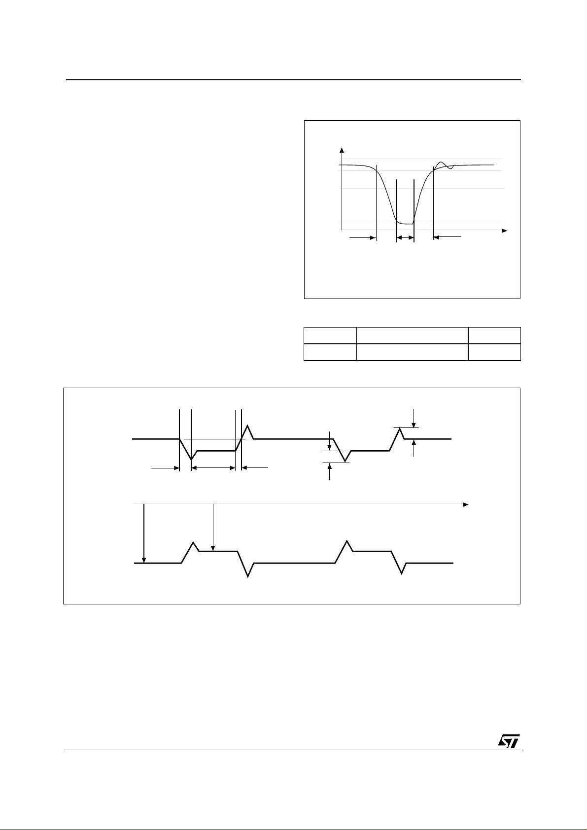
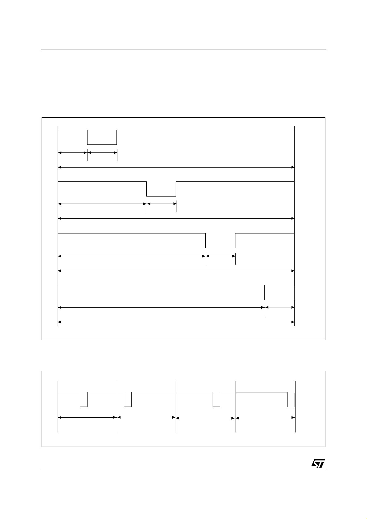
Communications between the VCD and the
LRI512 takes place using the modulation principle
of ASK (amplitude modulation). Two modulation
indices are used, 10% and 100%. The LRI512 decodes both. The VCD determines which index is
used.
The modulation index is defined as [a-b]/[a+b]
where a and b are the peak and minimum signal
amplitude, respectively, of the carrier frequency.
Depending of the choice made by the VCD, a
“pause” will be created as desc ribed in Figure 3
and Figure 4.
The LRI512 is operational for any de gree of m odulation index from between 10% and 30%.
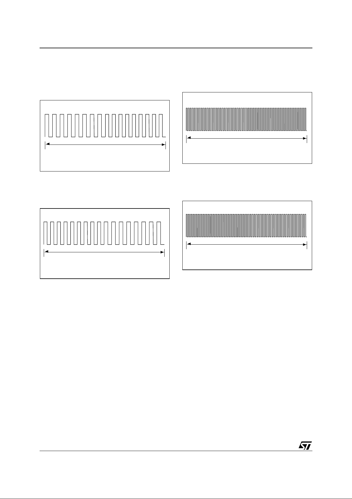
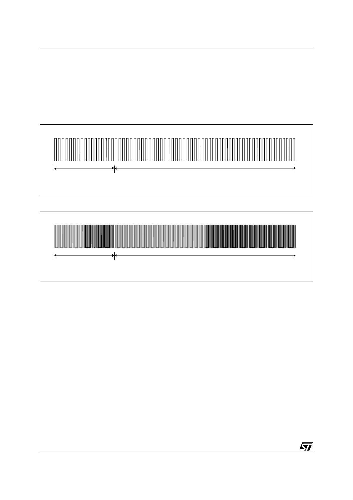
Figure 3. 100% Modulation Waveform
a
105%
100%
95%
60%
5%
tRFF
tRFR
tRFSBL
Table 3. 10% Modulation Parameters
hr 0.1 x (a-b) max
hf 0.1 x (a-b) max
t
AI06683
Figure 4. 10% Modulation Waveform
tRFF tRFSFL tRFR
ab t
hf
hr
AI06655
4/54
DATA RATE AND DATA CODING
The data coding implemented in the LRI512 uses
pulse position modulation. Both data coding
modes that are described in the ISO15693 are
supported by the LRI512. The sel ection is made
by the VCD and indicated to the LRI512 within the
Start of Frame (SOF).
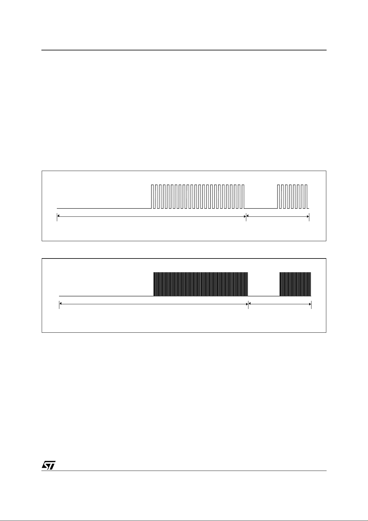
Data Coding Mode: 1 Out of 256
The value of one single byte is represented by the
position of one pause. Th e position of the pause
on 1 of 256 successive time period s of 18.88 µs
(256/f
), determines the value of the byte. In this
C
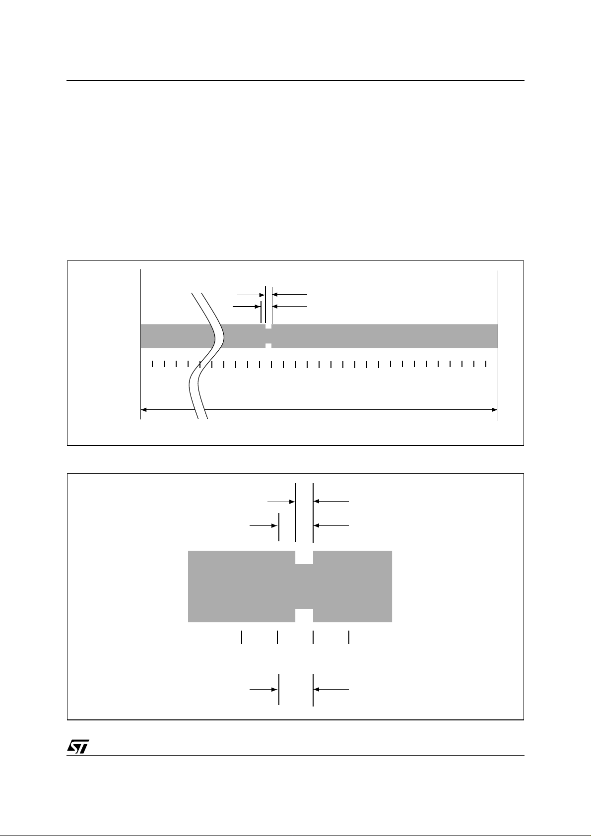
Figure 5. 1 Out of 256 Codin g Mode
Pulse
Modulated
Carrier
LRI512
case the transmission of one byte takes 4.833 ms
and the resulting data rate is 1.65 kbit/s (f
Figure 5 illustr ates t his puls e pos ition mo dulat ion
technique. In this figure, data E1h (225d) is sent by
the VCD to the LRI512.
The pause shall occur during the second half of
the position of the t ime pe riod t hat de term ines the
value, as shown in Figure 6.
A pause during the first period transmit the data
value 00h. A pause during the last period transmits
the data value FFh (255d).
9.44 µs
18.88 µs
/8192).
C
0 1 2 3 . . . . . . . . 2 . . . . . . . . . . . . . . . . . . . . . 2 2 2 2
. . . . . . . . . 2 . . . . . . . . . . . . . . . . . . . . . 5 5 5 5
. . . . . . . . . 5 . . . . . . . . . . . . . . . . . . . . . 2 3 4 5
Figure 6. Detai l of One Time Period
Pulse
Modulated
Carrier
4.833 ms
AI06656
9.44 µs
18.88 µs
. . . . . . .. . . . . . .
2
2
4
2
2
5
2
2
6
Time Period
one of 256
AI06657
5/54
LRI512
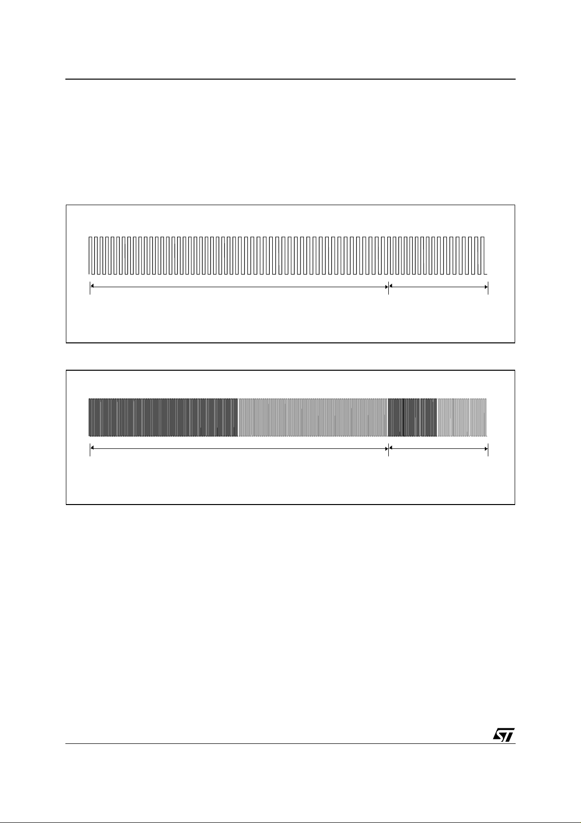
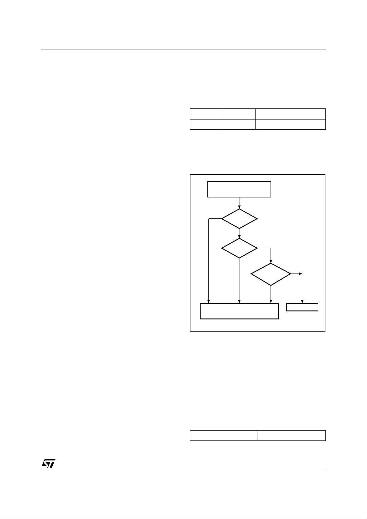
Data Coding Mode: 1 Out of 4
The value of 2 bits is represented by the position
of one pause. The position of the pause on 1 of 4
successive time periods of 18.88 µs (256/f
), de-
C
termines the value of the 2 bi ts. Four succes sive
Figure 7. 1 Out of 4 Coding Mode
Pulse position for "00"
9.44 µs 9.44 µs
Pulse position for "01" (1=LSB)
28.32 µs 9.44 µs
Pulse position for "10" (0=LSB)
pairs of bits form a byte, where the least significant
pair of bits is transmitted first.
In this case the transmission of one byte takes
302.08 µs and the resulting data rate is 26.48 kbit/
/512). Fig ure 7 illustr ates the 1 out o f 4 pulse
s (f
C
position technique and coding.
75.52 µs
75.52 µs
Pulse position for "11"
For example Figure 8 shows the transmission of
E1h (225d, 1110 0001b) by the VCD.
Figure 8. 1 Out of 4 Coding Exampl e
10
75.52 µs
00
75.52 µs
47.20µs 9.44 µs
75.52 µs
66.08 µs 9.44 µs
75.52 µs
AI06658
01 11
75.52 µs 75.52 µs
AI06659
6/54
LRI512
VCD to LRI512 Frames
Frames are delimited by a Start of Frame (SOF)
and an End of Frame (EOF) and are implemented
using code violation. Unused options are reserved
for fu tu r e u s e .
The LRI512 is ready to receive a new command
frame from the VCD after a delay of t
after having
2
sent a response frame to the VCD (as specified in
Table 59).
The LRI512 generates a Power-on delay of t
MINCD
after being activated by the powering field (as
specified in Table 59). After this delay, the LRI512
is ready to receive command frames from the
VCD.
Start of Frame (SOF)
The SOF defines the data codi ng mode the V CD
is to use for the following command frame.
The SOF sequence described in Figure 9 selects
the 1 out of 256 data coding mode.
The SOF sequence described in Figure 10 selects
the 1 out of 4 data coding mode.
The EOF sequence for either coding mode is described in Figure 11.
Figure 9. SOF to Select 1 Out of 256 Data Coding Mode
9.44 µs
37.76 µs
37.76 µs
9.44 µs
AI06661
Figure 10. SOF to Select 1 Out of 4 Data Coding Mode
9.44 µs
37.76 µs
9.44 µs
Figure 11. EOF for Either Data Co ding Mod e
9.44 µs
37.76 µs
9.44 µs
9.44 µs
37.76 µs
AI06660
AI06662
7/54
LRI512
COMMUNICATIONS SIGNAL FROM LRI512 TO VCD
For some parameters several modes have been
defined in order to allow for use in different noise
environments and application requirements.
Load Modulation
The LRI512 is capable of communication to the
VCD via an inductive couplin g area in which the
carrier is loaded to generate a s ubcarrier with frequency f
ing in a load in the LRI512.
Subcarri er
The LRI512 supports the one subcarrier and two
subcarriers response formats. These formats are
selected by the VCD using the first bit in the protocol header.
When one subcarrier is used, the frequency f
the subcarrier load m odulation is 423.75kHz ( f
32).
When two subcarriers are used, the frequency f
is 423.75 kHz (f
484.28 kHz (f
. The subcarrier is generated by switch-
S
S
/32), and the frequency fS2 is
C
/28). When using the two subcarri-
C
1 of
C
S
/
1
ers mode, the LRI512 generates a continuous
phase relationship between f
1 and fS2.
S
Data Rates
The LRI512 can respond using the low or the high
data rate format. The selection of the data rate is
made by the VCD using the s econd bi t in t he protocol header.
Table 4 shows the different data rates the LRI512
can achieve using each combination.
Table 4. Response Data Rate
Data Rate One Subcarrier Two Subcarriers
Low
High
6.62 kbit/s
/2048)
(f
C
26.48 kbit/s
/512)
(f
C
6.67 kbit/s
(fC/2032)
26.69 kbit/s
(fC/508)
8/54
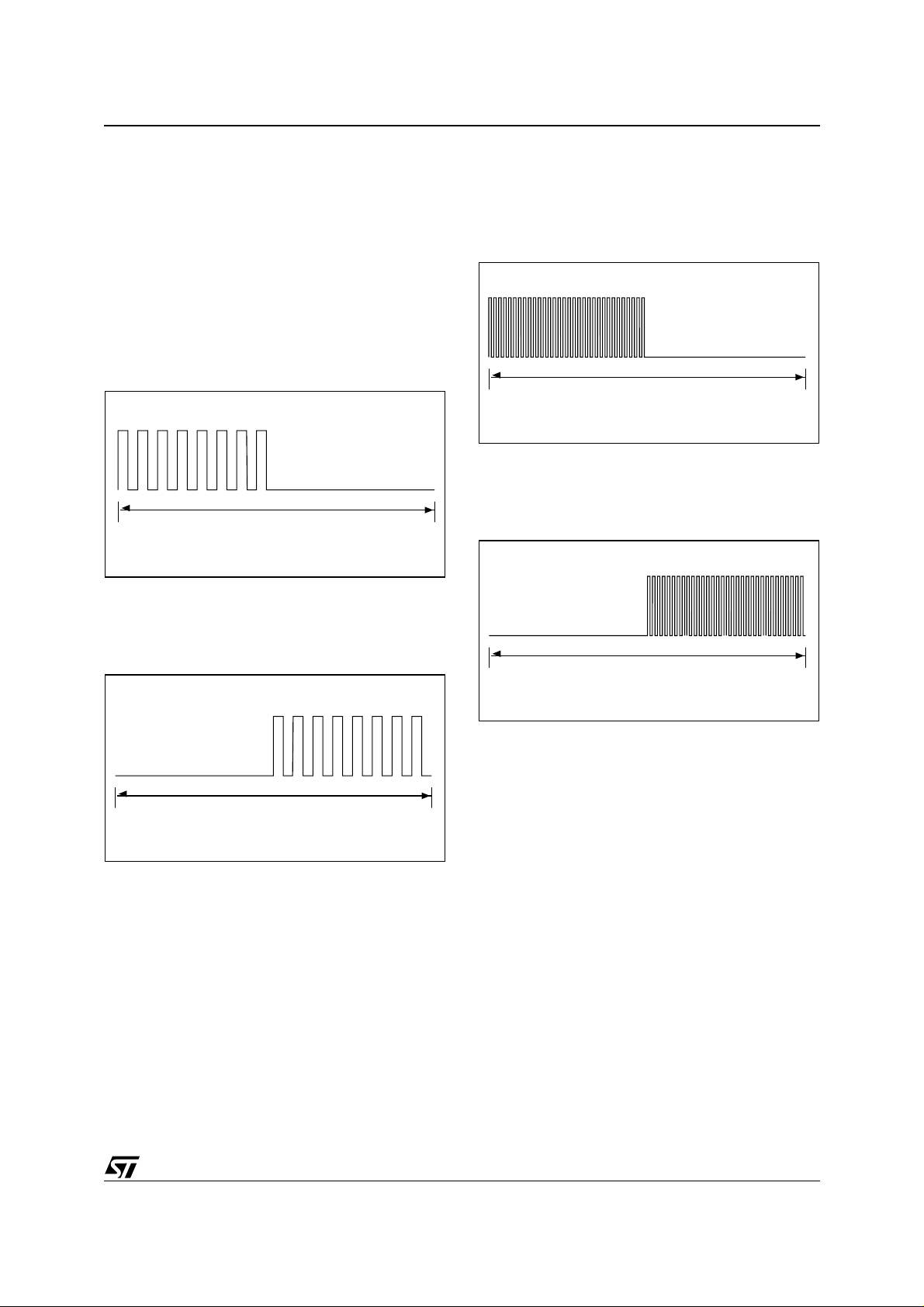
BIT REPRESENTATION AND CODING
Data bits are encoded usin g Manchester coding,
according to the following schemes.
For the low data rate the same subcarrier frequency or frequencies are used, in this case the num ber of pulses shall be multiplied by 4 and all times
will increas e b y thi s fa cto r .
Bit Coding Using One Subcarrier
High Data Rate. A logic 0 starts with 8 pulses of
423.75 kHz (f
/32) followed by an unmodulated
C
time of 18,88µs as shown in Figure 12.
LRI512
Low Data Rate. A logic 0 starts with 32 pulses of
423.75 kHz (fC/32) followed by an unmodulated
time of 75.52 µs as shown in Figure 14.
Figure 14. Logi c 0, Lo w D ata Ra te
Figure 12. Lo gi c 0 , Hi gh D at a R at e
37.76 µs
AI06663
A logic 1 starts with an unmodulated time of
18.88 µ s followed by 8 pulses of 423.75 kHz (f
C
32) as shown in Figure 13.
Figure 13. Lo gi c 1 , Hi gh D at a R at e
37.76 µs
AI06664
149.86 µs (ISO=151.04 µs)
A logic 1 starts with an unmodulated time of
75.52 µ s followed by 32 pulses of 423.75 kHz (f
32) as shown in Figure 15.
Figure 15. Logi c 1, Lo w D ata Ra te
/
149.86 µs (ISO=151.04 µs)
AI06666
AI06665
/
C
9/54
LRI512
Bit Coding Usi ng Two Subcarri ers
High Data Rate. A logic 0 starts with 8 pulses of
423.75 kHz (f
484.28 kHz (f
/32) followed by 9 pulses of
C
/28) as shown in Figure 16.
C
Figure 16. Lo gi c 0, Hi gh D a ta Ra te
37.46 µs
AI06670
A logic 1 starts with 9 pulses of 484.28 kHz (f
followed by 8 pulses of 423.75 kHz (f
C
/32) as
C
/28)
shown in Figure 17.
Figure 17. Lo gi c 1 , Hi gh D at a R at e
Low Data Rate. A logic 0 starts with 32 pulses of
423.75 kHz (f
484.28 kHz (f
/32) followed by 36 pulses of
C
/28) as shown in Figure 18.
C
Figure 18. Logic 0, Low Data Rate
149.86 µs ± 0.3 µs
AI06668
A logic 1 starts with 36 pulses of 484.28 k Hz (f
28) followed by 32 pulses of 423.75 kHz (f
/32) as
C
C
shown in Figure 19.
Figure 19. Logic 1, Low Data Ra te
/
37.46 µs
149.86 µs ± 0.3 µs
AI06667
AI06669
10/54
LRI512 TO VCD FRAMES
Frames are delimited by an SOF and EOF and are
implemented using code violation. Unused options
are reserved for future use.
For the low data rate, the same subcarrier frequency or frequencies are used. In this case the
number of pulses shall be multiplied by 4.
The VCD is ready to receive a response frame
from the LRI512 w ithin less than t
after having
1
sent a command frame (as specified in Table 59).
SOF Wh en U si ng One Subcarri er
High Data Rate. SOF comprises 3 parts: (see
Figure 20)
– an unmodulated time of 56.64 µs,
– 24 pulses of 423.75 kHz (
– a logic 1 which starts with an unmodulated time
of 18.88 µs followed by 8 pulses of 423.75 kHz.
Low Data Rate. SOF comprises 3 parts: (see
Figure 21)
– an unmodulated time of 226.56 µs,
– 96 pulses of 423.75 kHz (
– a logic 1 which starts with an unmodulated time
of 75.52 µs followed by 32 pulses of
423.75 kHz.
Figure 20. Start of Frame, High Data Rate, One Subcarrier
113.28 µs 37.76 µs
f
c
f
c
LRI512
/32),
/32),
AI06671
Figure 21. Start of Frame, Low Data Rate, One Subcarrier
453.12 µs 149.86 µs (ISO=151.04 µs)
AI06672
11/54
LRI512
SOF When U si ng Two Subcarri er s
High Data Rate. SOF comprises 3 parts: (see
Figure 22)
f
– 27 pulses of 484.28 kHz (
– 24 pulses of 423.75 kHz (
c
f
c
/28),
/32),
– a logic 1 which starts with 9 pulses of
484.28 kHz followed by 8 pulses of 423.75 kHz.
Low Data Rate. SOF comprises 3 parts: (see
Figure 23)
– 108 pulses of 484.28 kHz (
– 96 pulses of 423.75 kHz (
– a logic 1 which starts with 36 pulses of
484.28 kHz followed by 32 pulses of
423.75 kHz.
Figure 22. Start of Frame, High Data Rate, Two Subcarriers
112.39 µs 37.76 µs (ISO=37.46 µs)
Figure 23. Start of Frame, Low Data Rate, Two Subcarriers
f
c
f
/28),
c
/32),
AI06673
449.56 µs
149.86 µs ± 0.3 µs
AI06674
12/54
LRI512
EOF When Us i ng On e Su bc arrier
High Data Rate. EOF comprises 3 parts: (see
Figure 24)
– a logic 0 which starts with 8 pulses of
423.75 kHz followed by an unmodulated time of
18.88 µs.
f
– 24 pulses of 423.75 kHz (
/32),
c
Low Data Rate. EOF comprises 3 parts: (see
Figure 25)
– a logic 0 which starts with 32 pulses of
423.75 kHz followed by an unmodulated time of
75.52 µs.
– 96 pulses of 423.75 kHz (
– an unmodulated time of 226.56 µs.
– an unmodulated time of 56.64 µs.
Figure 24. End of Frame, High Data Rate, One Subcarrier
37.76 µs
Figure 25. End of Frame, Low Data Rate, One Subcarrier
113.28 µs
f
c
/32),
AI06675
453.12 µs151.04 µs
AI06676
13/54
LRI512
EOF When U si ng Two Subcarri er s
High Data Rate. EOF comprises 3 parts: (see
Figure 26)
– a logic 0 which starts with 8 pulses of
423.75 kHz followed by 9 pulses of 484.28 kHz,
– 24 pulses of 423.75 kHz (
– 27 pulses of 484.28 kHz (
f
c
f
c
/32),
/28).
Low Data Rate. EOF comprises 3 parts: (see
Figure 27)
– a logic 0 which starts with 32 pulses of
423.75 kHz followed by 36 pulses of
484.28 kHz,
– 96 pulses of 423.75 kHz (
– 108 pulses of 484.28 kHz (
Figure 26. End of Frame, High Data Rate, Two Subcarriers
112.39 µs37.46 µs
Figure 27. End of Frame, Low Data Rate, Tw o S ubcar riers
f
c
/32),
f
/28).
c
AI06677
449.56 µs151.62 µs (ISO=149.86 µs)
AI06678
14/54
UNIQUE IDENTIFIER (UID)
The LRI512s are uniquely identified by a 64-bit
Unique Identifier (UID). This UID complies with
ISO/IEC 15963 and ISO/IEC 7816-6. The UID is a
read only code, and comprises:
– The 8 MSB is E0h
– The IC Ma nufacturer code of ST 02h, o n 8 bits
(ISO/IEC 7816-6/AM1)
– A Unique Serial Number on 48 bits.
The UID is used for addressing each LRI512
uniquely and individu ally, during the ant i-collision
APPLICATION FAMILY IDENTIFIER (AFI)
The AFI (Application Family Identifier) describes
the type of application targeted by the VCD, and is
used to extract from all the LRI512 s present only
the LRI512s meeting the required application criteria .
It is programmed by the LRI512 issuer in the AFI
register. Once programmed and Locked, it cannot
be modified.
The most significant ni bble of A FI i s used to code
one specific or all application families.
The least significant nibble of AFI i s used to code
one specific or all application sub-families. Subfamily codes, other than 0, are proprietary.
(See ISO 15693-3 documentation)
LRI512
loop and for one-to-one exchange between a VCD
and a LRI512.
Table 5. UID Format
MSB LSB
63 56 55 48 47 0
E0h 02h Unique Serial Number
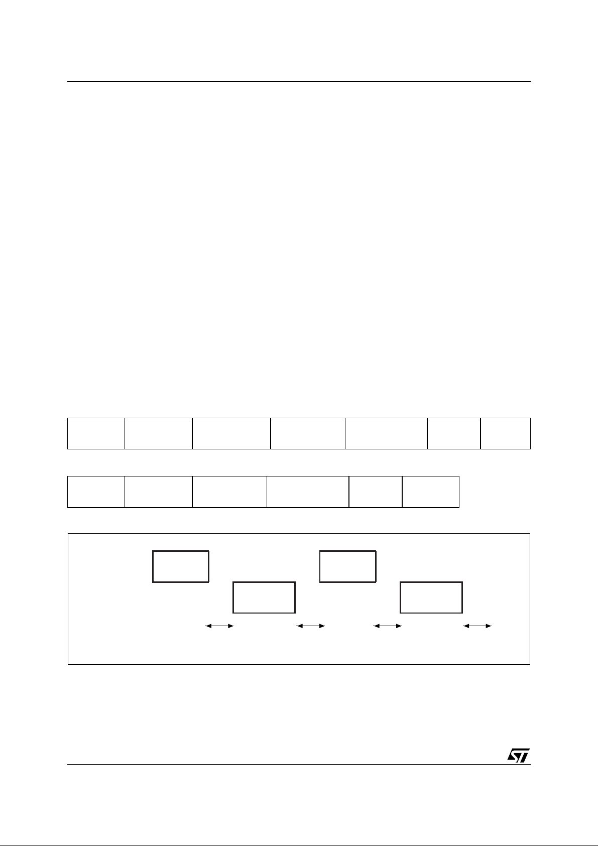
Figure 28. LRI512 Decision Tree for AFI
Inventory Request
Received
No
AFI Flag
Set ?
Yes
AFI value
= 0 ?
Yes
No
AFI value
= Internal
value ?
No
CRC
The CRC used in the LRI512 is calculated as per
the definition in ISO/IEC 13239.
The initial register content is all ones: FFFFh.
The 2-byte CRC is appended to each Request and
each Response, within each frame, before the
EOF. The CRC is calculated on all the bytes after
the SOF up to the CRC field.
Upon reception of a Request from the VCD, the
LRI512 verifies that the CRC value is valid. If it is
invalid, it discards the frame, and does not answer
the VCD.
Upon reception of a Response from the LRI512, it
is recommended that the VCD verify that the CRC
Yes
Answer given by the LRI512
to the Inventory Request
No Answer
AI06679
value is valid. If it is invalid, actions to be performed are left to the responsibility of the VCD designer.
The CRC is transmitted Least Significant Byte first.
Each byte is transmitted Least Significant Bit first.
Table 6. CRC Transmission Rules
LSByte MSByte
LSBit MSBit LSBit MSBit
CRC 16 (8bits) CRC 16 (8 bits)
15/54
LRI512
LRI512 PROTOCOL DESCRIPTI ON
The Transmission protocol defines the mechanism to exchange instructions and data between
the VCD and the LRI512, in both directions.
It is based on the concept of “VCD talks first”.
This means that any LRI51 2 does n ot start trans-
mitting unless it has received and properly decoded an instruction sent by the VCD.
The protocol is based on an exchange of
– a Request from the VCD to the LRI512
– a Response from the LRI512 to the VCD
Each Request and each Response is contained in
a Frame. The frame delimiters (SOF, EOF) are described in the previous paragraphs.
Each Request consists of
– Request SOF (see Figure 9 and Figure 10)
– Flags
– A Command Code
– Parameters, depending on the Command
– Application data
– 2-byte CRC
– Request EOF (see Figure 11)
Each Response consists of
– Answer SOF (see Figure 20 to Figure 23)
– Flags
– Parameters, depending on the Command
– Application data
– 2-byte CRC
– Answer EOF (see Figure 24 to Figure 27)
The protocol is bit-oriented. The number of bits
transmitted in a frame is a multiple o f eight (8) –
that is, an integer number of bytes.
A single-byte field is transm itted Least Significant
Bit (LSBit) first.
A multiple-byte field is transmitted Least Significant Byte (LSByte) first, each byte is transmitted
Least Significant Bit (LSBit) first.
The setting of the flags indicates the pres ence of
the optional fields. When the flag is s et (to one),
the field is present. When the flag is reset (to zero),
the field is absent.
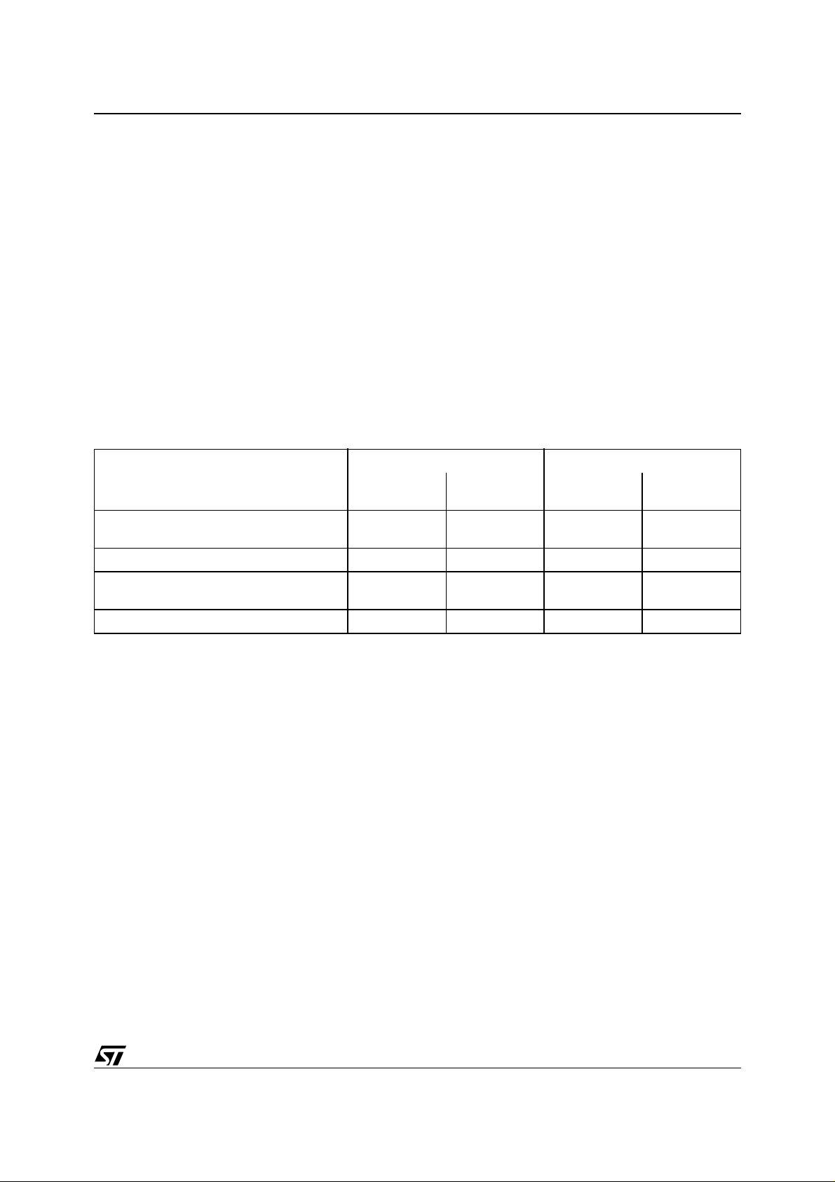
Table 7. VCD Request Frame Format
Request
SOF
Request Flags Command Code Parameters Data
Table 8. LRI512 Response Fr ame Fo rm at
Response
SOF
Response
Flags
Parameters Data
Figure 29. LRI512 Protocol Timing
VCD
LRI512
Timing
Request Frame
(Table 7)
Response Frame
(Table 8)
t1 t2 t1 t2
2 Bytes
CRC
Request Frame
(Table 7)
2 Bytes
CRC
Response
EOF
Response Frame
(Table 8)
Request
EOF
AI06830
16/54
LRI512 STATES
A LRI512 can be in one of four states:
– Power-off
– Ready
– Quiet
–Selected
Transitions between these s tates are specified in
Figure 30 and Table 9.
Power-off State
The LRI512 is in t he Power-of f state when it does
not receive enough energy from the VCD.
Quiet State
When in the Quiet State, the LRI512 answe rs any
Request other than an Inventory Request with the
Address_Flag set.
Selected State
In the Selected State, the LR I512 answers to any
Request in all modes:
– Request in Select mode with the Select flag set
– Request in Addressed mode if the UID match.
– Request in Non-Addressed mode as it is gener-
al Request.
Ready State
The LRI512 is in the Ready state when it receives
enough energy from the V CD. It sha ll ans wer any
Request where the Select_Flag is not set.
Table 9. LRI512 Response, Depending on the States of the Request Flags
Address_Flag Select_Flag
Flags
LRI512 in Ready or Selected state (Devices
in Quiet state do not answer)
LRI512 in Selected state X X
1
Addressed0Non Addressed
XX
Selected
LRI512
1
0
Non Selected
LRI512 in Ready, Quiet or Selected state (the
device which match the UID)
Error (03h) X X
XX
17/54
 Loading...