

LOW DROP VOLTAGE REGULATOR DRIVE
FOR EXTERNAL N-CHANNEL POWER MOSFET
■ VERYLOW DROPOUTPOWERMOSFET
DRIVER
■ HIGHPRECISIONVref= 2.5V(± 2%)
■
VERYLOW CURRENTDRAIN(TYP.2mA)
■ REFERENCEOUTPUTCURRENT UP TO
20mA
■
OPERATINGSUPPLYVOLTAGEFROM5V
TO30V
■
MAXIMUM INPUTVOLTAGEON-GATEPIN
(N.8) UP TO 60V
■ INTERNAL CURRENTLIMIT OPERATIONAL
AMPLIFIEROFFSETTRIMMED AT
50mV
± 10mV
■
NOCAPACITOR IS NEEDED FORSTABILITY
OFREFERENCE OUTPUT
■ TEMPERATURERANGE0
APPLICATION
■ ULTRAHIGH CURRENT ULTRA LOW
DROPOUTVOLTAGEREGULATOR
■ CONSTANTHIGH CURRENTSOURCE
o
CTO70oC
LPR30
DIP-8 SO-8
■ LOWPARTSCOUNT 5V TO 3.3V
COMPUTERSUPPLY
■ LOWNOISE/LOWDROPSMPSPOST
REGULATOR
DESCRIPTION
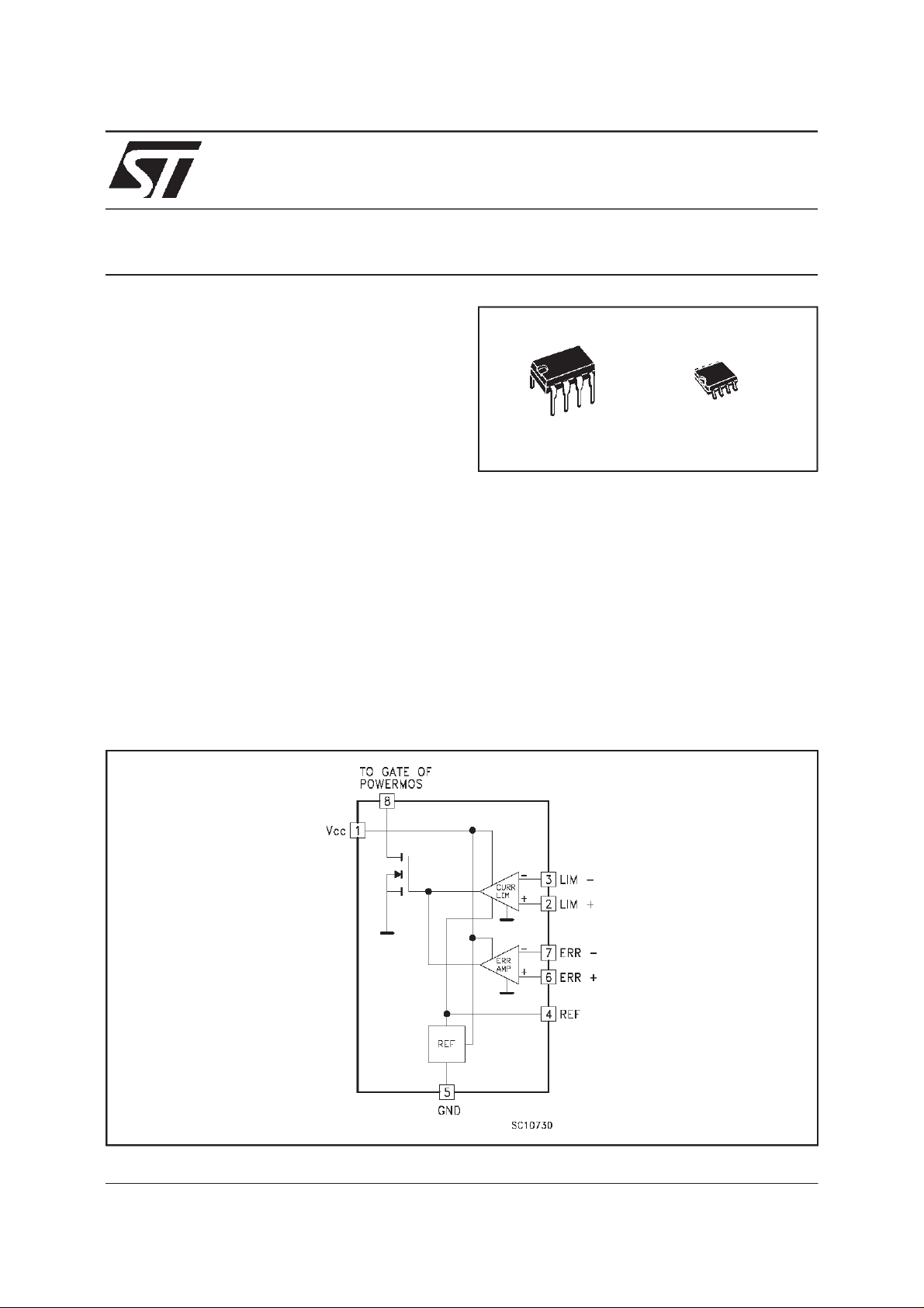
The LPR30 is a very Low Dropout Regulator
Controller in a single IC solution for very high
current low dropout linear voltgage regulator. It
uses an external N-CHANNEL POWER MOSFET
as the linear passelement. The LPR30 features a
dropout voltage as low as the R
DS(on)
of the
BLOCKDIAGRAM
May 2000
1/10
LPR30
external Power MOSFET multiplied by the output
current. Consequently the output current can be
as high as the POWER MOSFET can provide
(also using an adeguate heatsink).
The V
of the LPR30 range from 5V to 30V. For
CC
very low drop voltage operation,the LPR30
requires an external gate drive supply to provide
the control voltage needed to drive the gate of the
externalPOWERMOSFET.
The regulator output is constant-current limited
when the controller detects 50mV across an
externalsense resistor.
It has an internal high precision (± 2%) Voltage
Referenceat 2.5V
The output regulated voltage is possible to
program to any voltage from 1V to more than
50V.
Flexible design is achieved by the availability of
the Voltage Reference Output through an
externalpin (N.4) that is able to supply morethan
20mA as load current. The LPR30 is available in
8 pin plastic DIP and in SO-8 for SMD. In both
packageversions it isable to operate from 0
o
C.
70
ABSOLUTE MAXIMUM RATINGS
Symbol Parameter Value Unit
V
I
V
I
Absolute Maximum Ratings are those values beyond which damage to the device may occur.
Functionaloperation under these conditions is not implied.
DC InputVoltage 36 V
CC
Reference OutputCurrent Internally Limited
oREF
PowerDissipation 1 W
P
tot
Operating JunctionTemperature Range 0 to 70
T
op
T
Storage Temperature Range - 40 to 150
stg
Maximum GateVoltage(pin n8) 60 V
gate
Maximum GateCurrent(pin n8) 200 mA
gate
o
Cto
o
C
o
C
THERMALDATA
Symbol Parameter DIP-8 SO-8 Unit
R
thj-amb
(*) This value depends from thermal design of PCB on which the device is mounted.
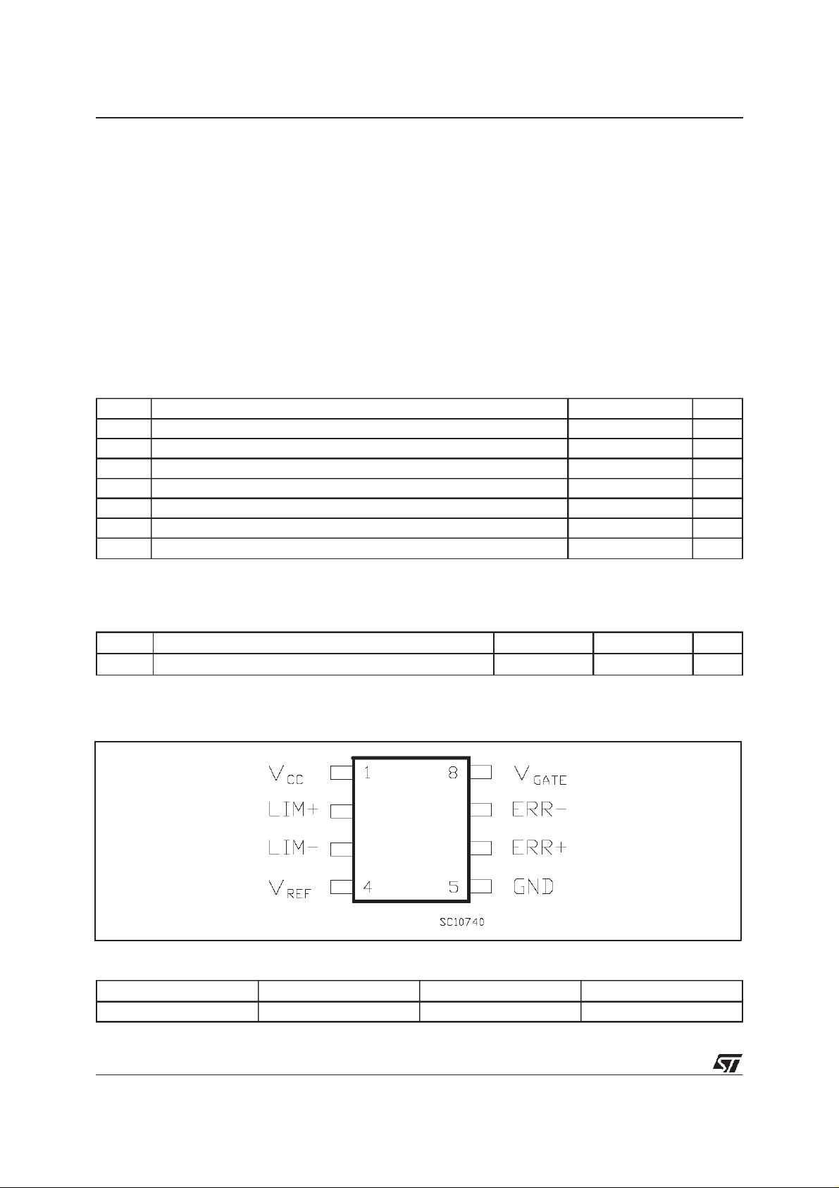
CONNECTION DIAGRAM
Thermal Resistance Junction-ambient (*) Max 130 to 180 100 to 150
(topview)
o
ORDERING NUMBERS
Type DIP-8 SO-8 SO-8 (tape & reel)
LPR30 LPR30N LPR30D LPR30D-TR
C/W
2/10
ELECTRICAL CHARACTERISTICS
(Referto thetestcircuits, V
=10V, Tj=25oC unlessotherwise specified.
CC
GENERAL
Symbol Parameter Test Conditions Min. Typ. Max. Unit
V
I
CC
Operating SupplyVoltage 5 30 V
CC
SupplyCurrent IK=0µAVCC=30V
= 0 to70oC
T
j
24mA
ERR(-),LIM(-)= 1V
ERR(+),LIM(+)= 0V
V
OSAT
OutputSaturation Voltage VCC=5V IO=100mA
T
= 0 to70oC
j
280 500 mV
ERR(-),LIM(-)= 1V
ERR(+),LIM(+)= 0V
I
OLK
OutputLeakage Current VCC=5V VO=60V
100
ERR(-),LIM(-)= 0V
ERR(+),LIM(+)= 1V
REFERENCE BLOCK
Symbol Parameter Test Conditions Min. Typ. Max. Unit
V
REF
I
∆V
REF
SVR SupplyVoltage Rejection V
eN OutputNoise B = 10 Hz to 10 KHz
Reference OutputVoltage 2.45 2.5 2.55 V
Reference OutputCurrent 20 mA
K
/∆IKReference OutputVoltage
IK= 1 to 20 mA C
= 0 pF 3 mV
REF
Change
<10V±1V f = 120 Hz C
IN
= 0 pF 70 dB
REF
50
I
=10mA C
K
REF
=0pF
LPR30
A
µ
V
µ
ERRORAMPLIFIER BLOCK
Symbol Parameter Test Conditions Min. Typ. Max. Unit
I
V
I
OS
G
V
InputBiasCurrent 0.3 1
B
InputOffsetVoltage VCC= 5 to30 V Tj=0 to 70oC5mV
OS
InputOffsetCurrent 5 50 nA
Open LoopGain Tj= 0 to70oC80dB
V
InputCommonMode Voltage
CM
Tj= 0 to70oC1V
-1 V
CC
Range
CMR Common ModeRejection 70 dB
SVR SupplyVoltage Rejection V
=9 to11V f = 120Hz
IN
=9 to11V f = 10KHz
V
IN
70
60
CURRENT LIMITING BLOCK
Symbol Parameter Test Conditions Min. Typ. Max. Unit
I
V
G
V
InputBiasCurrent 0.5
B
InputOffsetVoltage Tj= 0 to70oC4060V
OS
Open LoopGain Tj= 0 to70oC50dB
V
InputCommonMode Voltage
CM
Tj= 0 to70oC0V
-3 V
CC
Range
µ
dB
dB
µ
A
A
3/10
 Loading...