

SINGLE J-FET OPERATIONAL AMPLIFIER
.INTERNALLY ADJUSTABLE INPUT OFFSET
VOLTAGE
.LOW POWER CONSUMPTION
.WIDE COMMON-MODE (UP TO V
DIFFERENTIALVOLTAGERANGE
CC
+
)AND
.LOW INPUT BIAS AND OFFSET CURRENT
.OUTPUTSHORT-CIRCUIT PROTECTION
.HIGH INPUT IMPEDANCE J–FET INPUT
STAGE
.INTERNAL FREQUENCY COMPENSATION
.LATCHUPFREE OPERATION
.HIGHSLEWRATE: 16V/µs (typ)
DESC RIP TI ON
Thesecircui t sare highspeedJ–FETinputsingle
operationalampl if iersinc or poratingw el lmatched,high
voltage J–FET and bipolar transistors in a monolithic
integratedcircui t.
Thedevicesfeaturehighslewrates,lowinputbiasand
offsetcurr ents, and lowoffsetvoltagetemperatur e
coefficient .
LF251 - LF351
WIDE BANDWIDTH
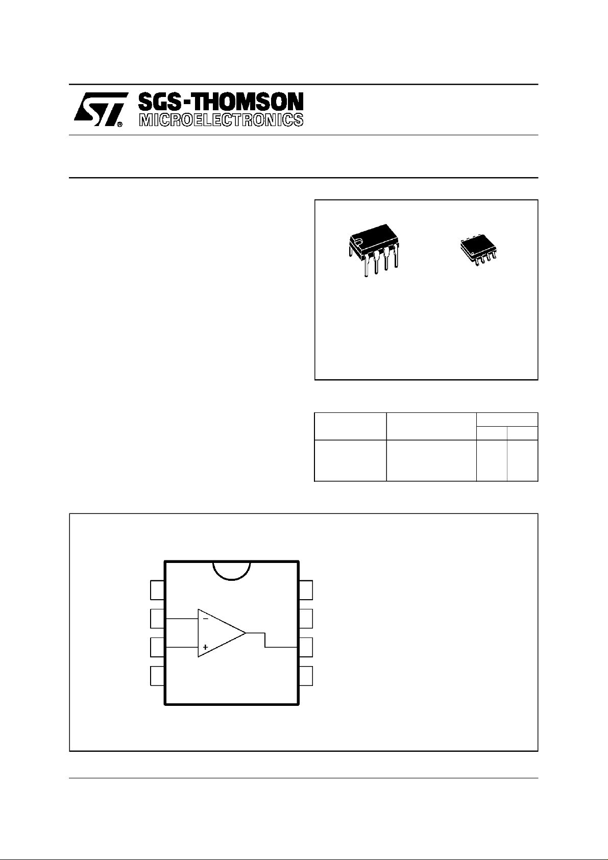
N
DIP8
(PlasticPackage)
ORDER CODES
Part Number Temperature
o
LF351 0
LF251 –40
LF151 –55
C, +70oC ••
o
C, +105oC ••
o
C, +125oC ••
LF15 1
D
SO8
(PlasticMicropackage)
Package
ND
PIN CONNECTI O NS (top view)
1
2
3
4
October1997
8
7
6
1 - Offset Null 1
2 - Inverting input
3 - Non-inverting input
-
4-V
CC
5 - Offset Null 2
6 - Output
+
7-V
CC
8 - N.C.
5
1/9
LF151 - LF251 - LF351
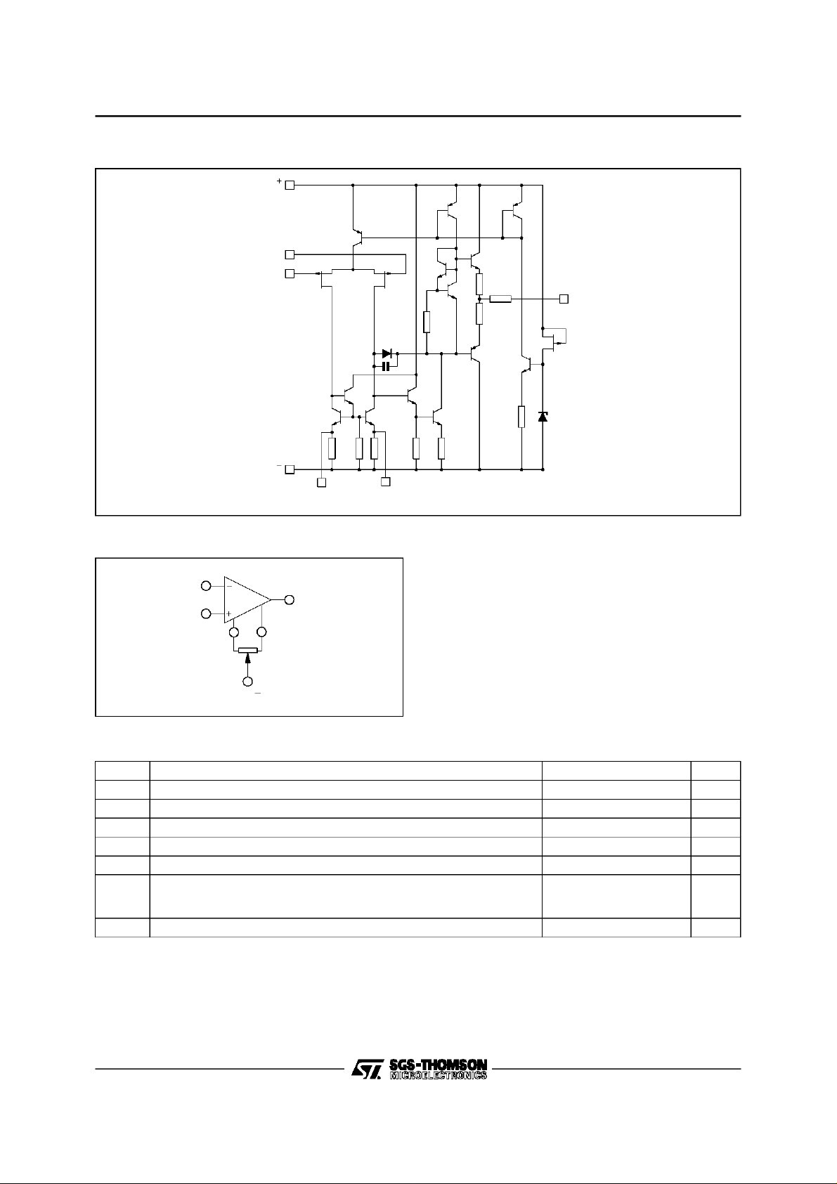
SCHE MATIC DI AGRAM
Non-inverting
Inve rting
V
CC
input
input
1.3k
V
CC
Offse t Null1 Offset Null2
Ω
100
100
30k
Ω
1.3k
35k
100
35k
Ω
200
Ω
8.2k
Output
INPUT OFFS ET VOLTAG E NULL CIRCUITS
LF35 1
N1
N2
Ω
100k
V
CC
ABSOLUTE MAXIMUM RATINGS
Symbol Parameter Value Unit
V
P
T
T
Notes: 1. All voltagevalues, except differential voltage, are with respect to the zero reference level (ground)of the supplyvoltageswhere the
Supply Voltage - (note 1) ±18 V
CC
Input Voltage - (note 3) ±15 V
V
i
Differential Input Voltage - (note 2) ±30 V
V
id
Power Dissipation 680 mW
tot
Output Short-circuit Duration - (note 4) Infinite
Operating Free Air Temperature Range LF351
oper
LF251
LF151
Storage Temperature Range –65 to 150
stg
zero reference levelis the midpoint between V
2. Differentialvoltages are at the non-inverting input terminalwith respect to the inverting input terminal.
3. The magnitude of the inputvoltage must never exceed themagnitude of the supply voltage or 15 volts, whichever is less.
4. The output may be shorted to ground or to either supply. Temperature and /or supply voltages must be limitedto ensure that the
dissipationrating is not exceeded.
+
CC
andV
–
.
CC
0to70
–40 to 105
–55 to 125
o
C
o
C
2/9
LF151 - LF251 - LF351
ELECTRICAL CHARACTERISTICS
= ±15V, T
V
CC
Symbol Parameter
V
DV
A
Input Offset Voltage (RS= 10kΩ)
io
Input Offset Voltage Drift 10 µV/oC
io
Input Offset Current *
I
io
Input Bias Current *
I
ib
Large Signal Voltage Gain (RL=2kΩ,VO=±10V)
vd
SVR Supply Voltage Rejection Ratio (R
I
V
Supply Current (no load)
CC
Input Common Mode Voltage Range ±11 +15
icm
CMR Common Mode Rejection Ratio (R
Ios Output Short-circuit Current
±V
Output Voltage Swing
OPP
SR Slew Rate
(V
t
Rise Time
r
(V
K
OV
Overshoot
(V
GBP Gain Bandwidth Product
(f = 100kHz, T
R
Input Resistance 10
i
THD Total Harmonic Distortion (f = 1kHz, A
C
L
e
Equivalent Input Noise Voltage (f = 1kHz, Rs= 100Ω)15
n
∅m Phase Margin 45 Degrees
* The inputbias currents arejunction leakage currents which approximately double forevery 10oC increase in thejunctiontemperature.
=25oC (unless otherwise specified)
amb
=25oC
T
amb
≤ T
T
min.
T
amb
T
min.
T
amb
T
min.
T
amb
T
min.
T
amb
T
min.
T
amb
T
min.
T
amb
T
min.
T
amb
T
min.
T
amb
T
min.
= 10V, RL=2kΩ, CL= 100pF, T
i
= 20mV, RL=2kΩ,CL= 100pF, T
i
= 20mV, RL=2kΩ,CL= 100pF, T
i
= 100pF, T
≤ T
amb
max.
=25oC
≤ T
≤ T
amb
max.
=25oC
≤ T
≤ T
amb
max.
=25oC
≤ T
≤ T
amb
max.
= 10kΩ)
=25oC
≤ T
amb
≤ T
max.
S
=25oC
≤ T
≤ T
amb
max.
= 10kΩ)
=25oC
≤ T
amb
≤ T
max.
S
=25oC
≤ T
≤ T
amb
max.
=25oCR
≤ T
≤ T
amb
max.
=25oC, Vin= 10mV, RL=2kΩ,CL= 100pF) 2.5 4
amb
=25oC, VO=2VPP) 0.01
amb
=2kΩ
L
= 10kΩ
R
L
RL=2kΩ
= 10kΩ
R
L
=25oC, unity gain) 12 16
amb
=25oC, unity gain) 0.1
amb
amb
= 20dB, RL=2kΩ,
V
LF151 - LF251 - LF351
Min. Typ. Max.
20 200
50
200
25
80
86
80
1.4 3.4
-12
70
86
70
10
40 60
10
10
12
12
13.5
10
12
=25oC, unity gain) 10
310
13
5 100
4
20
3.4
60
12
Unit
mV
pA
nA
pA
nA
V/mV
dB
mA
V
dB
mA
V
V/µs
µs
%
MHz
Ω
%
nV
√Hz
3/9
 Loading...