

Datasheet LF45ABPT-TR, LF45ABDT-TR, LF47CDT-TR, LF47ABPT-TR, LF45CPT-TR Datasheet (SGS Thomson Microelectronics)
...
1/34August 2003
■ VERY LOW DROPOUT VOLTAGE (0.45V)
■ VERY LOW QUIESCENT CURRENT (TYP.
50 µA IN OFFMODE,500 µA IN ON MODE)
■ OUTPUT CURRENT UP TO 500 mA
■ LOGIC-CONTROLLED ELECTRONIC
SHUTDOWN
■ OUTPUT VOLTAGES OF 1.25; 1.5; 1.8; 2.5;
2.7; 3; 3.3; 3.5; 4; 4.5; 4.7; 5; 5.2; 5.5; 6; 8;
8.5; 9; 12V
■ INTERNAL CURRENT AND THERMAL LIMIT
■ ONLY 2 .2 µF FOR STABILITY
■ AVAILABLE IN ± 1% (AB) OR ± 2% (C)
SELECTION AT 25 °C
■ SUPPLY VOLTAGE REJECTION: 80db (TYP. )
■ TEMPERATURE RANGE: -40 TO 12 5 °C
DESCRIPTION
The LF00 series are very Low Drop regulators
available in PENTAWA TT, TO-220, TO-220FP ,
DPAK and PPAK package and in a wide range of
output voltages.
The very Low Drop voltage (0.45V) and the very
low quiescent current make them particularly
suitable for Low Noise, Lo w Power applications
and specially in battery powered systems.
In the 5 pins configuration (PENTAW AT T and
PPAK) a Shutdown Logic Control function is
available (pin 2, TTL compatible). This means that
when the device is used as a local regulator, it is
possible to put a part of the board in standby,
decreasing the tot al power consumption. In t he
three terminal configuration the device has the
same electricalperformance, but is fixed in the ON
state. It requires only a 2.2 µF capacitor for
stability allowing space and cost saving.
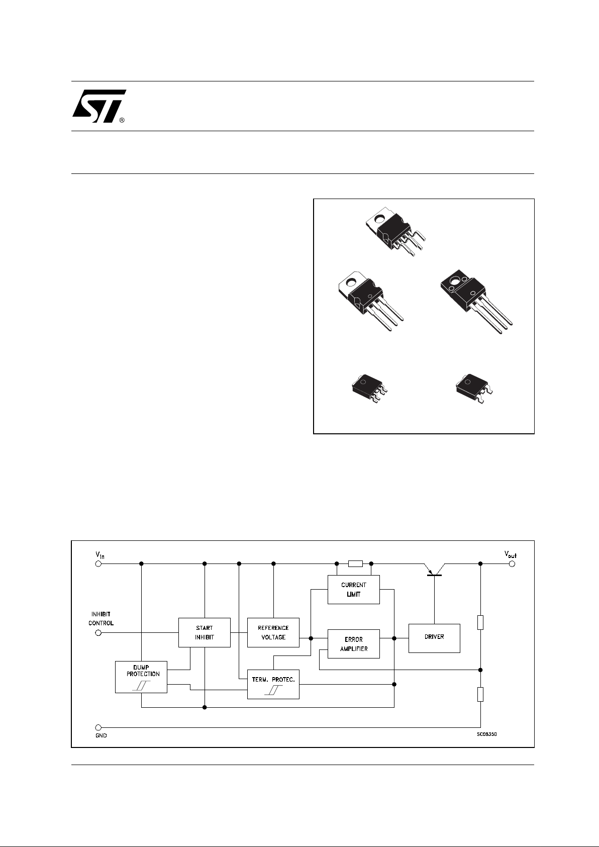
LF00
SERIES
VERY LOW DROP
VOLTAGE REGULATORS WITH INHIBIT
SCHEMATIC DIAGRAM
TO-220
PENTAWATT
DPAKPPAK
TO-220FP
LF00 SERIES
2/34
ABSOLUTE MAXIMUM RATINGS
(*) For 18 < VIN< 40 the regulator is in shut-down
THERMAL DATA
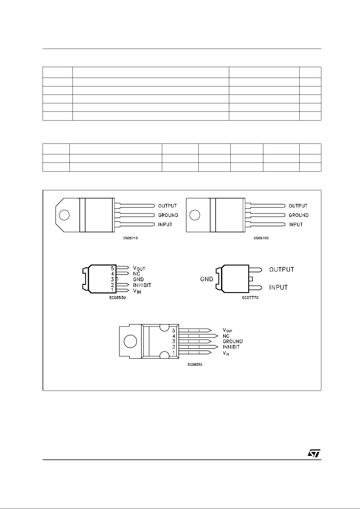
CONNECTION DIAGRAM (t op v iew)
Symbol Parameter Value Unit
V
I
DC Input Voltage
-0.5 to 40 (*) V
I
O
Output Current
Internally Limited
P
tot
Power Dissipation
Internally Limited
T
stg
Storage Temperature Range
-40 to 150 °C
T
op
Operating Junction Temperature Range
-40 to 125 °C
Symbol Parameter PENTAWATT TO-220 TO-220FP DPAK/PPAK Unit
R
thj-case
Thermal Resistance Junction-case
3358°C/W
R
thj-amb
Thermal Resistance Junction-ambient
50 50 60 100 °C/W
TO-220 TO-220FP
DPAK
PPAK
PENTAWATT
LF00 SERIES
3/34
ORDERING CODES
(*) Available on request.
(#) Available in Tape & Reel with the suffix "-TR".
TYPE PENTAWATT TO-220 TO-220FP DPAK (#) PPAK (#)
OUTPUT
VOLTAGE
LF12C (*) LF12CV5V LF12CV LF12CP LF12CDT LF12CPT 1.25 V
LF12AB (*) LF12ABV5V LF12ABV LF12ABP LF12ABDT LF12ABPT 1.25 V
LF15C LF15CV5V (*) LF15CV (*) LF15CP (*) LF15CDT LF15CPT (*) 1.5 V
LF15AB LF15ABV5V (*) LF15ABV (*) LF15ABP (*) LF15ABDT LF15ABPT (*) 1.5 V
LF18C LF18CV5V LF18CV LF18CP LF18CDT LF18CPT 1.8 V
LF18AB LF18ABV5V LF18ABV LF18ABP LF18ABDT LF18ABPT 1.8 V
LF25C LF25CV5V LF25CV LF25CP LF25CDT LF25CPT 2.5 V
LF25AB LF25ABV5V LF25ABV LF25ABP LF25ABDT LF25ABPT 2.5 V
LF27C LF27CV5V LF27CV LF27CP LF27CDT LF27CPT 2.7 V
LF27AB LF27ABV5V LF27ABV LF27ABP LF27ABDT LF27ABPT 2.7 V
LF30C LF30CV5V LF30CV LF30CP LF30CDT LF30CPT 3 V
LF30AB LF30ABV5V LF30ABV LF30ABP LF30ABDT LF30ABPT 3 V
LF33C LF33CV5V LF33CV LF33CP LF33CDT LF33CPT 3.3 V
LF33AB LF33ABV5V LF33ABV LF33ABP LF33ABDT LF33ABPT 3.3 V
LF35C LF35CV5V LF35CV LF35CP LF35CDT LF35CPT 3.5 V
LF35AB LF35ABV5V LF35ABV LF35ABP LF35ABDT LF35ABPT 3.5 V
LF40C LF40CV5V LF40CV LF40CP LF40CDT LF40CPT 4 V
LF40AB LF40ABV5V LF40ABV LF40ABP LF40ABDT LF40ABPT 4 V
LF45C (*) LF45CV5V LF45CV LF45CP LF45CDT LF45CPT 4.5 V
LF45AB (*) LF45ABV5V LF45ABV LF45ABP LF45ABDT LF45ABPT 4.5 V
LF47C LF47CV5V LF47CV LF47CP LF47CDT LF47CPT 4.75 V
LF47AB LF47ABV5V LF47ABV LF47ABP LF47ABDT LF47ABPT 4.75 V
LF50C LF50CV5V LF50CV LF50CP LF50CDT LF50CPT 5 V
LF50AB LF50ABV5V LF50ABV LF50ABP LF50ABDT LF50ABPT 5 V
LF52C LF52CV5V LF52CV LF52CP LF52CDT LF52CPT 5.2 V
LF52AB LF52ABV5V LF52ABV LF52ABP LF52ABDT LF52ABPT 5.2 V
LF55C LF55CV5V LF55CV LF55CP LF55CDT LF55CPT 5.5 V
LF55AB LF55ABV5V LF55ABV LF55ABP LF55ABDT LF55ABPT 5.5 V
LF60C LF60CV5V LF60CV LF60CP LF60CDT LF60CPT 6 V
LF60AB LF60ABV5V LF60ABV LF60ABP LF60ABDT LF60ABPT 6 V
LF80C LF80CV5V LF80CV LF80CP LF80CDT LF80CPT 8 V
LF80AB LF80ABV5V LF80ABV LF80ABP LF80ABDT LF80ABPT 8 V
LF85C LF85CV5V LF85CV LF85CP LF85CDT LF85CPT 8.5 V
LF85AB LF85ABV5V LF85ABV LF85ABP LF85ABDT LF85ABPT 8.5 V
LF90C LF90CV5V LF90CV LF90CP LF90CDT LF90CPT 9 V
LF90AB LF90ABV5V LF90ABV LF90ABP LF90ABDT LF90ABPT 9 V
LF120C LF120CV5V LF120CV LF120CP LF120CDT LF120CPT 12 V
LF120AB LF120ABV5V LF120ABV LF120ABP LF120ABDT LF120ABPT 12 V
LF00 SERIES
4/34
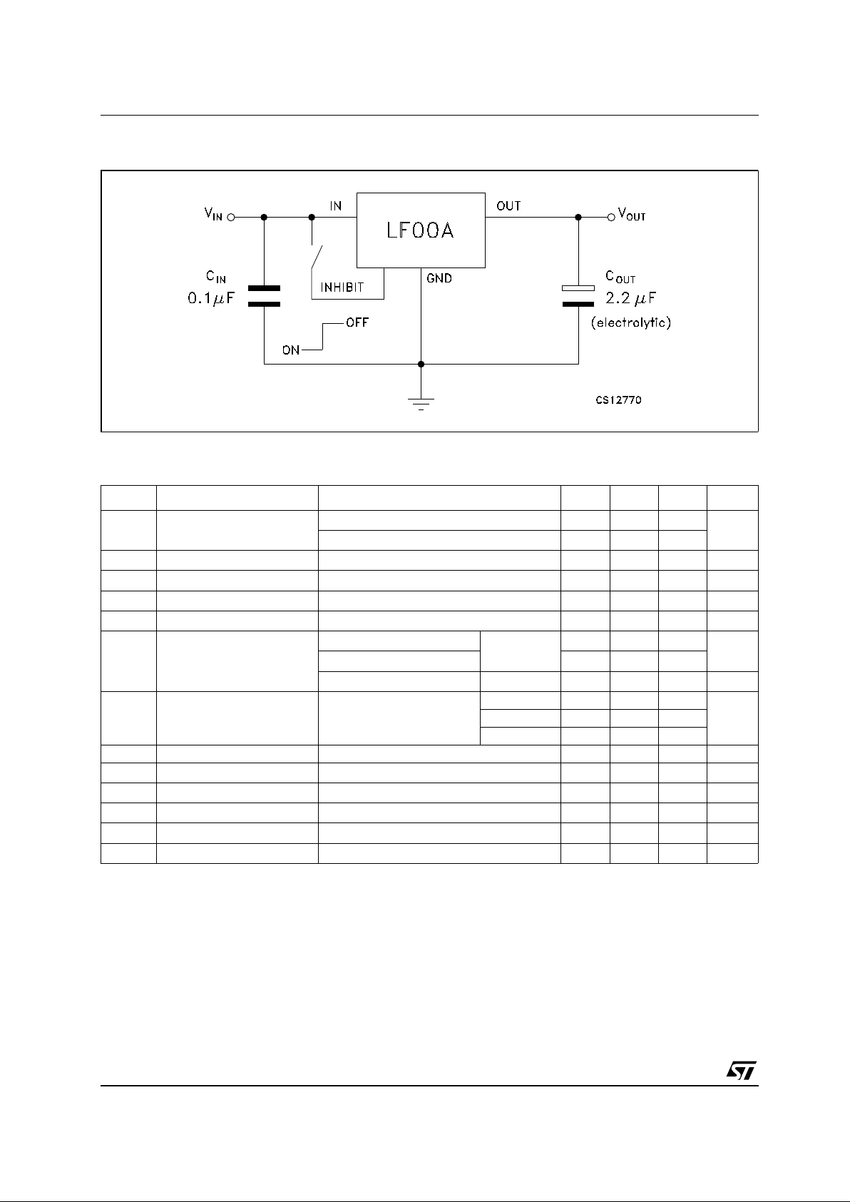
TEST CIRCUITS
ELECTRICAL CHARACTERISTICS FOR LF12AB (refer to the test circuits, T
j
=25°C,CI=0.1µF,
C
O
=2.2µF unless otherwise specified.)
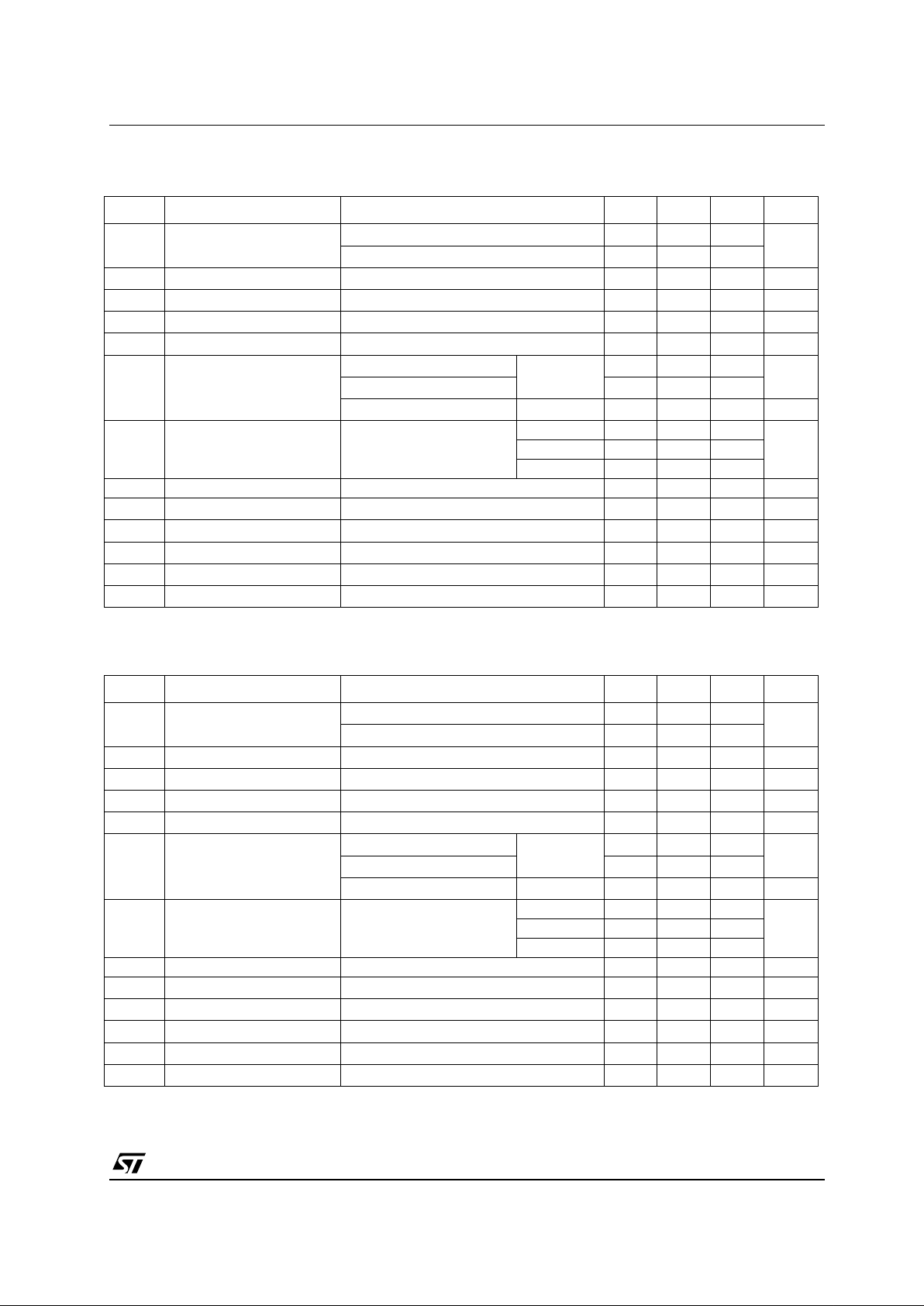
Symbol Parameter Test Conditions Min. Typ. Max. Unit
V
O
Output Voltage IO= 50 mA, VI= 3.3 V 1.238 1.25 1.263 V
I
O
= 50 mA, VI =3.3V,Ta= -25 to 85°C 1.225 1.275
V
I
Operating Input Voltage IO= 500 mA 2.5 16 V
I
O
Output Current Limit 1 A
∆V
O
Line Regulation VI = 2.5 to 16 V, IO= 5 mA 2 10 mV
∆V
O
Load Regulation VI = 2.8 V IO= 5 to 500 mA 2 10 mV
I
d
Quiescent Current VI = 2.5 to 16V, IO= 0mA ON MODE 0.5 1 mA
V
I
= 2.6 to 16V, IO= 500mA 12
V
I
= 6 V OFF MODE 50 100 µA
SVR Supply Voltage Rejection I
O
=5mA
V
I
= 3.5 ± 1 V
f = 120 Hz 82 dB
f=1KHz 77
f = 10 KHz 65
eN Output Noise Voltage B = 10 Hz to 100 KHz 50 µV
V
d
Dropout Voltage IO= 200 mA 1.25 V
V
IL
Control Input Logic Low Ta= -40 to 125°C 0.8 V
V
IH
Control Input Logic High Ta= -40 to 125°C 2 V
I
I
Control Input Current VI =6V, VC =6V 10 µA
C
O
Output Bypass Capacitance ESR = 0.1 to 10 Ω IO=0to500mA 2 10 µF
LF00 SERIES
5/34
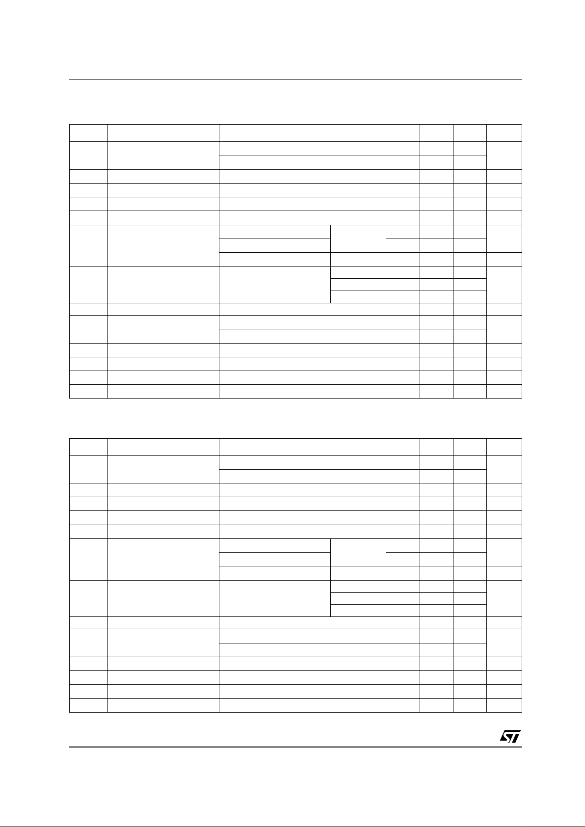
ELECTRICAL CHARACTERISTICS FOR LF12C (refer to the test circuits, Tj=25°C,CI=0.1µF,
C
O
=2.2µF unless otherwise specified.)
ELECTRICAL CHARACTERISTICS FOR LF15AB (refer to the test circuits, T
j
=25°C,CI=0.1µF,
C
O
=2.2µF unless otherwise specified.)
Symbol Parameter Test Conditions Min. Typ. Max. Unit
V
O
Output Voltage IO= 50 mA, VI= 3.3 V 1.225 1.25 1.275 V
I
O
= 50 mA, VI = 3.3 V, Ta= -25 to 85°C 1.2 1.3
V
I
Operating Input Voltage IO= 500 mA 2.5 16 V
I
O
Output Current Limit 1 A
∆V
O
Line Regulation VI = 2.5 to 16 V, IO= 5 mA 2 10 mV
∆V
O
Load Regulation VI = 2.8 V IO= 5 to 500 mA 2 10 mV
I
d
Quiescent Current VI = 2.5 to 16V, IO= 0mA ON MODE 0.5 1 mA
V
I
= 2.6 to 16V, IO= 500mA 12
V
I
= 6 V OFF MODE 50 100 µA
SVR Supply Voltage Rejection I
O
=5mA
V
I
=3.5±1V
f = 120 Hz 82 dB
f = 1 KHz 77
f = 10 KHz 65
eN Output Noise Voltage B = 10 Hz to 100 KHz 50 µV
V
d
Dropout Voltage IO= 200 mA 1.25 V
V
IL
Control Input Logic Low Ta= -40 to 125°C 0.8 V
V
IH
Control Input Logic High Ta= -40 to 125°C 2 V
I
I
Control Input Current VI =6V, VC =6V 10 µA
C
O
Output Bypass Capacitance ESR = 0.1 to 10 Ω IO= 0 to 500 mA 2 10 µF
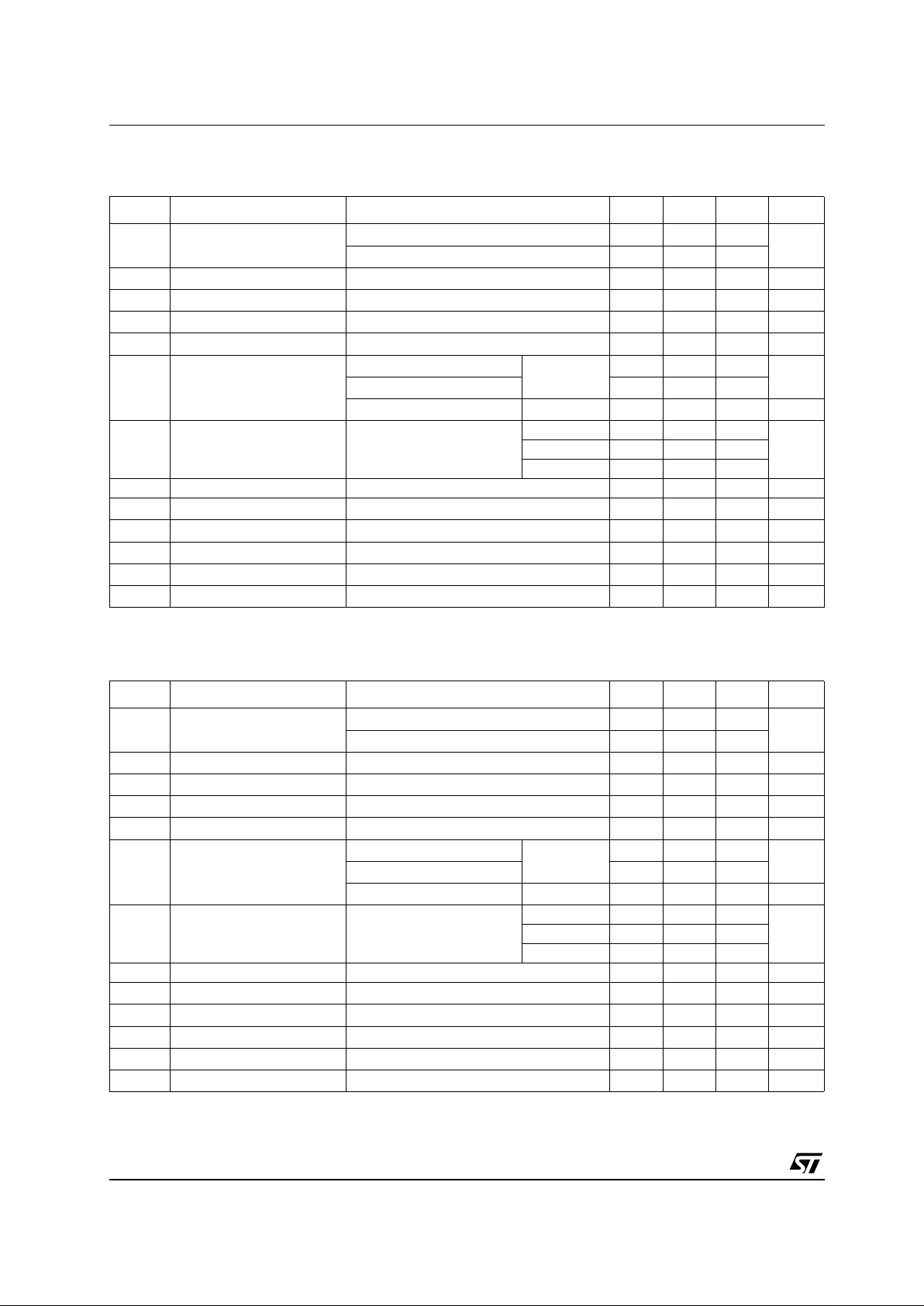
Symbol Parameter Test Conditions Min. Typ. Max. Unit
V
O
Output Voltage IO= 50 mA, VI= 3.5 V 1.485 1.5 1.515 V
I
O
= 50 mA, VI = 3.5 V, Ta= -25 to 85°C 1.470 1.530
V
I
Operating Input Voltage IO= 500 mA 2.5 16 V
I
O
Output Current Limit 1 A
∆V
O
Line Regulation VI = 2.5 to 16 V, IO= 5 mA 2 10 mV
∆V
O
Load Regulation VI = 2.8 V, IO= 5 to 500 mA 2 10 mV
I
d
Quiescent Current VI = 2.5 to 16V, IO= 0mA ON MODE 0.5 1 mA
V
I
= 2.8 to 16V, IO= 500mA 12
V
I
= 6 V OFF MODE 50 100 µA
SVR Supply Voltage Rejection I
O
=5mA
V
I
=3.5±1V
f = 120 Hz 82 dB
f = 1 KHz 77
f = 10 KHz 65
eN Output Noise Voltage B = 10 Hz to 100 KHz 50 µV
V
d
Dropout Voltage IO=200mA 1 V
V
IL
Control Input Logic Low Ta= -40 to 125°C 0.8 V
V
IH
Control Input Logic High Ta= -40 to 125°C 2 V
I
I
Control Input Current VI =6V, VC =6V 10 µA
C
O
Output Bypass Capacitance ESR = 0.1 to 10 Ω IO= 0 to 500 mA 2 10 µF
LF00 SERIES
6/34
ELECTRICAL CHARACTERISTICS FOR LF15C (refer to the test circuits, Tj= 25°C, CI=0.1µF,
C
O
=2.2µF unless otherwise specified.)
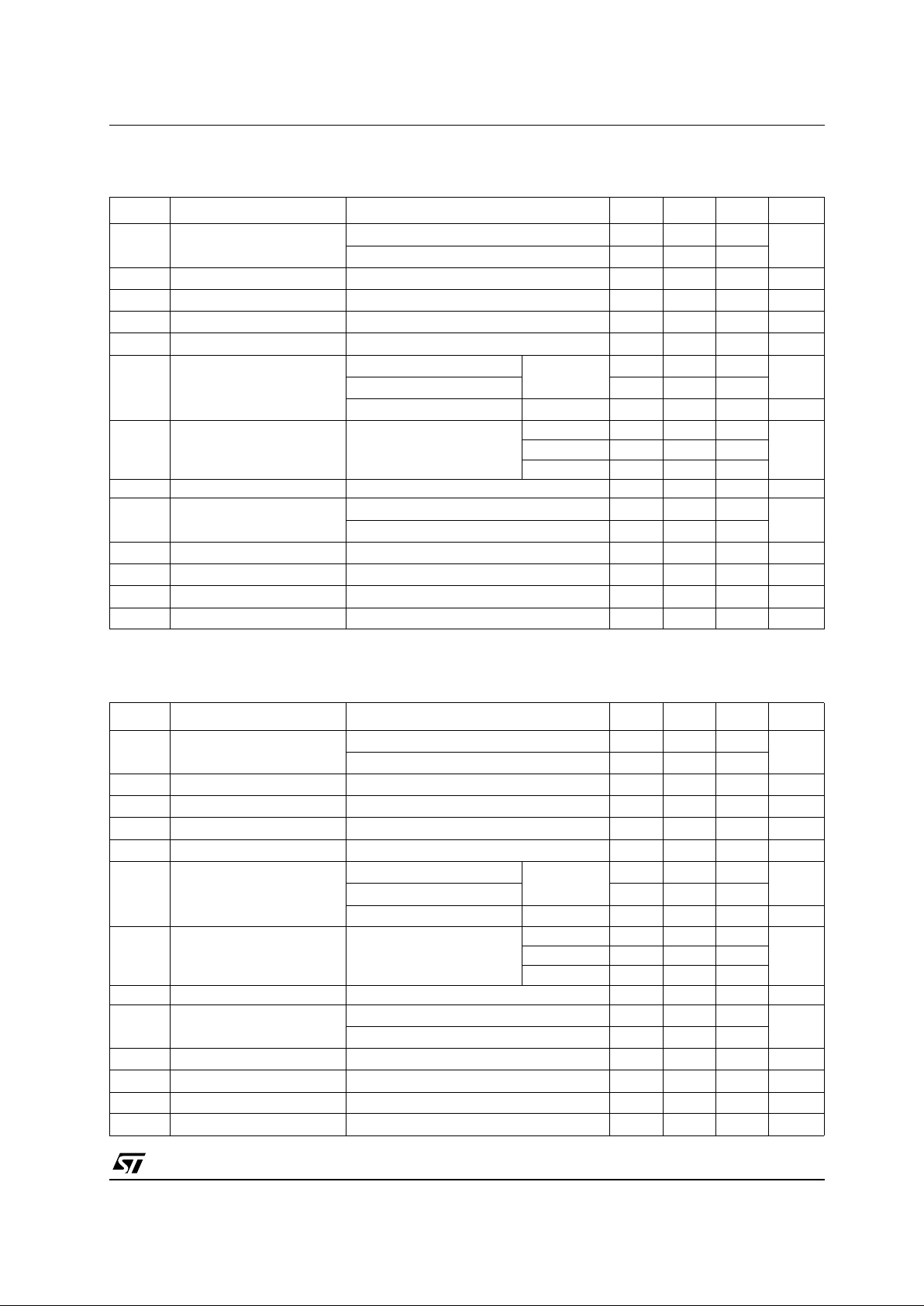
ELECTRICAL CHARACTERISTICS FOR LF18AB (refer to the test circuits, T
j
=25°C,CI=0.1µF,
C
O
=2.2µF unless otherwise specified.)
Symbol Parameter Test Conditions Min. Typ. Max. Unit
V
O
Output Voltage IO= 50 mA, VI= 3.5 V 1.47 1.5 1.53 V
I
O
= 50 mA, VI =3.5V,Ta= -25 to 85°C 1.44 1.56
V
I
Operating Input Voltage IO= 500 mA 2.5 16 V
I
O
Output Current Limit 1 A
∆V
O
Line Regulation VI = 2.5 to 16 V, IO= 5 mA 2 10 mV
∆V
O
Load Regulation VI = 2.8 V, IO= 5 to 500 mA 2 10 mV
I
d
Quiescent Current VI = 2.5 to 16V, IO= 0mA ON MODE 0.5 1 mA
V
I
= 2.8 to 16V, IO= 500mA 12
V
I
= 6 V OFF MODE 50 100 µA
SVR Supply Voltage Rejection I
O
=5mA
V
I
= 3.5 ± 1 V
f = 120 Hz 82 dB
f=1KHz 77
f = 10 KHz 65
eN Output Noise Voltage B = 10 Hz to 100 KHz 50 µV
V
d
Dropout Voltage IO= 200 mA 1 V
V
IL
Control Input Logic Low Ta= -40 to 125°C 0.8 V
V
IH
Control Input Logic High Ta= -40 to 125°C 2 V
I
I
Control Input Current VI =6V, VC =6V 10 µA
C
O
Output Bypass Capacitance ESR = 0.1 to 10 Ω IO=0to500mA 2 10 µF
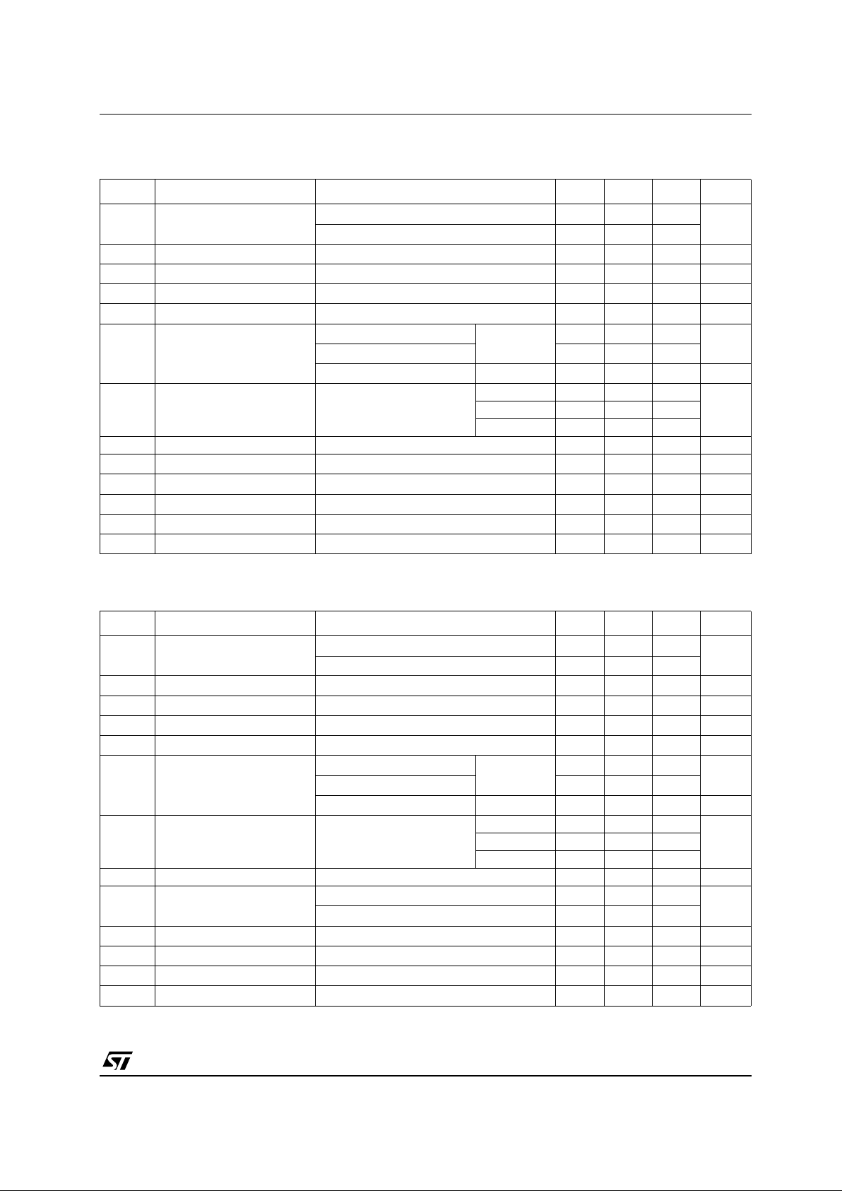
Symbol Parameter Test Conditions Min. Typ. Max. Unit
V
O
Output Voltage IO= 50 mA, VI= 3.3 V 1.782 1.8 1.818 V
I
O
= 50 mA, VI =3.3V,Ta= -25 to 85°C 1.764 1.836
V
I
Operating Input Voltage IO= 500 mA 3 16 V
I
O
Output Current Limit 1 A
∆V
O
Line Regulation VI = 2.8 to 16 V, IO= 5 mA 2 12 mV
∆V
O
Load Regulation VI = 3.3 V, IO= 5 to 500 mA 2 10 mV
I
d
Quiescent Current VI = 2.5 to 16V, IO= 0mA ON MODE 0.5 1 mA
V
I
= 3.1 to 16V, IO= 500mA 12
V
I
= 6 V OFF MODE 50 100 µA
SVR Supply Voltage Rejection I
O
=5mA
V
I
= 3.5 ± 1 V
f = 120 Hz 82 dB
f=1KHz 77
f = 10 KHz 60
eN Output Noise Voltage B = 10 Hz to 100 KHz 50 µV
V
d
Dropout Voltage IO= 200 mA 0.7 V
V
IL
Control Input Logic Low Ta= -40 to 125°C 0.8 V
V
IH
Control Input Logic High Ta= -40 to 125°C 2 V
I
I
Control Input Current VI =6V, VC =6V 10 µA
C
O
Output Bypass Capacitance ESR = 0.1 to 10 Ω IO=0to500mA 2 10 µF
LF00 SERIES
7/34
ELECTRICAL CHARACTERISTICS FOR LF18C (refer to the test circuits, Tj= 25°C, CI=0.1µF,
C
O
=2.2µF unless otherwise specified.)
ELECTRICAL CHARACTERISTICS FOR LF25AB (refer to the test circuits, T
j
=25°C,CI=0.1µF,
C
O
=2.2µF unless otherwise specified.)
Symbol Parameter Test Conditions Min. Typ. Max. Unit
V
O
Output Voltage IO= 50 mA, VI= 3.5 V 1.764 1.8 1.836 V
I
O
= 50 mA, VI =3.5V,Ta= -25 to 85°C 1.728 1.872
V
I
Operating Input Voltage IO= 500 mA 3 16 V
I
O
Output Current Limit 1 A
∆V
O
Line Regulation VI = 2.8 to 16 V, IO= 5 mA 2 12 mV
∆V
O
Load Regulation VI = 3.3 V, IO= 5 to 500 mA 2 10 mV
I
d
Quiescent Current VI = 2.5 to 16V, IO= 0mA ON MODE 0.5 1 mA
V
I
= 3.1 to 16V, IO= 500mA 12
V
I
= 6 V OFF MODE 50 100 µA
SVR Supply Voltage Rejection I
O
=5mA
V
I
= 3.5 ± 1 V
f = 120 Hz 82 dB
f=1KHz 77
f = 10 KHz 60
eN Output Noise Voltage B = 10 Hz to 100 KHz 50 µV
V
d
Dropout Voltage IO= 200 mA 0.7 V
V
IL
Control Input Logic Low Ta= -40 to 125°C 0.8 V
V
IH
Control Input Logic High Ta= -40 to 125°C 2 V
I
I
Control Input Current VI =6V, VC =6V 10 µA
C
O
Output Bypass Capacitance ESR = 0.1 to 10 Ω IO=0to500mA 2 10 µF
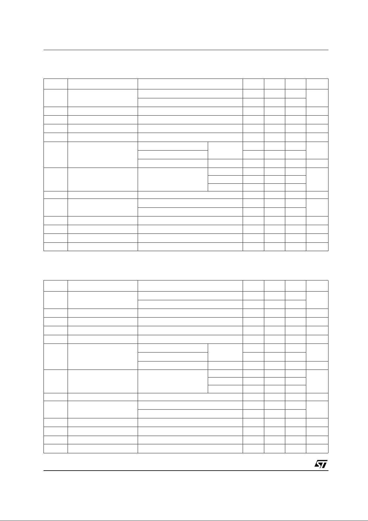
Symbol Parameter Test Conditions Min. Typ. Max. Unit
V
O
Output Voltage IO= 50 mA, VI= 4.5 V 2.475 2.5 2.525 V
I
O
= 50 mA, VI =4.5V,Ta= -25 to 85°C 2.450 2.550
V
I
Operating Input Voltage IO= 500 mA 16 V
I
O
Output Current Limit 1 A
∆V
O
Line Regulation VI = 3.5 to 16 V, IO= 5 mA 2 12 mV
∆V
O
Load Regulation VI = 3.8 V, IO= 5 to 500 mA 2 12 mV
I
d
Quiescent Current VI = 3.5 to 16V, IO= 0mA ON MODE 0.5 1 mA
V
I
= 3.8 to 16V, IO= 500mA 12
V
I
= 6 V OFF MODE 50 100 µA
SVR Supply Voltage Rejection I
O
=5mA
V
I
= 4.5 ± 1 V
f = 120 Hz 82 dB
f=1KHz 77
f = 10 KHz 65
eN Output Noise Voltage B = 10 Hz to 100 KHz 50 µV
V
d
Dropout Voltage IO= 200 mA 0.2 0.35 V
I
O
= 500 mA 0.4 0.7
V
IL
Control Input Logic Low Ta= -40 to 125°C 0.8 V
V
IH
Control Input Logic High Ta= -40 to 125°C 2 V
I
I
Control Input Current VI =6V, VC =6V 10 µA
C
O
Output Bypass Capacitance ESR = 0.1 to 10 Ω IO=0to500mA 2 10 µF
LF00 SERIES
8/34
ELECTRICAL CHARACTERISTICS FOR LF25C (refer to the test circuits, Tj= 25°C, CI=0.1µF,
C
O
=2.2µF unless otherwise specified.)
ELECTRICAL CHARACTERISTICS FOR LF27AB (refer to the test circuits, T
j
=25°C,CI=0.1µF,
C
O
=2.2µF unless otherwise specified.)
Symbol Parameter Test Conditions Min. Typ. Max. Unit
V
O
Output Voltage IO= 50 mA, VI= 4.5 V 2.45 2.5 2.55 V
I
O
= 50 mA, VI =4.5V,Ta= -25 to 85°C 2.4 2.6
V
I
Operating Input Voltage IO= 500 mA 16 V
I
O
Output Current Limit 1 A
∆V
O
Line Regulation VI = 3.5 to 16 V, IO= 5 mA 2 12 mV
∆V
O
Load Regulation VI = 3.8 V, IO= 5 to 500 mA 2 12 mV
I
d
Quiescent Current VI = 3.5 to 16V, IO= 0mA ON MODE 0.5 1 mA
V
I
= 3.8 to 16V, IO= 500mA 12
V
I
= 6 V OFF MODE 50 100 µA
SVR Supply Voltage Rejection I
O
=5mA
V
I
= 4.5 ± 1 V
f = 120 Hz 82 dB
f=1KHz 77
f = 10 KHz 65
eN Output Noise Voltage B = 10 Hz to 100 KHz 50 µV
V
d
Dropout Voltage IO= 200 mA 0.2 0.35 V
I
O
= 500 mA 0.4 0.7
V
IL
Control Input Logic Low Ta= -40 to 125°C 0.8 V
V
IH
Control Input Logic High Ta= -40 to 125°C 2 V
I
I
Control Input Current VI =6V, VC =6V 10 µA
C
O
Output Bypass Capacitance ESR = 0.1 to 10 Ω IO=0to500mA 2 10 µF
Symbol Parameter Test Conditions Min. Typ. Max. Unit
V
O
Output Voltage IO= 50 mA, VI= 4.7 V 2.673 2.7 2.727 V
I
O
= 50 mA, VI =4.7V,Ta= -25 to 85°C 2.646 2.754
V
I
Operating Input Voltage IO= 500 mA 16 V
I
O
Output Current Limit 1 A
∆V
O
Line Regulation VI = 3.7 to 16 V, IO= 5 mA 2 13 mV
∆V
O
Load Regulation VI =4V, IO= 5 to 500 mA 2 13 mV
I
d
Quiescent Current VI = 3.7 to 16V IO= 0mA ON MODE 0.5 1 mA
V
I
=4to16V IO= 500mA 12
V
I
= 6 V OFF MODE 50 100 µA
SVR Supply Voltage Rejection I
O
=5mA
V
I
= 4.7 ± 1 V
f = 120 Hz 82 dB
f=1KHz 77
f = 10 KHz 65
eN Output Noise Voltage B = 10 Hz to 100 KHz 50 µV
V
d
Dropout Voltage IO= 200 mA 0.2 0.35 V
I
O
= 500 mA 0.4 0.7
V
IL
Control Input Logic Low Ta= -40 to 125°C 0.8 V
V
IH
Control Input Logic High Ta= -40 to 125°C 2 V
I
I
Control Input Current VI =6V, VC =6V 10 µA
C
O
Output Bypass Capacitance ESR = 0.1 to 10 Ω IO=0to500mA 2 10 µF

LF00 SERIES
9/34
ELECTRICAL CHARACTERISTICS FOR LF27C (refer to the test circuits, Tj= 25°C, CI=0.1µF,
C
O
=2.2µF unless otherwise specified.)
ELECTRICAL CHARACTERISTICS FOR LF30AB (refer to the test circuits, T
j
=25°C,CI=0.1µF,
C
O
=2.2µF unless otherwise specified.)
Symbol Parameter Test Conditions Min. Typ. Max. Unit
V
O
Output Voltage IO= 50 mA, VI= 4.7 V 2.646 2.7 2.754 V
I
O
= 50 mA, VI =4.7V,Ta= -25 to 85°C 2.592 2.808
V
I
Operating Input Voltage IO= 500 mA 16 V
I
O
Output Current Limit 1 A
∆V
O
Line Regulation VI = 3.7 to 16 V IO= 5 mA 2 13 mV
∆V
O
Load Regulation VI =4V, IO= 5 to 500 mA 2 13 mV
I
d
Quiescent Current VI = 3.7 to 16V IO= 0mA ON MODE 0.5 1 mA
V
I
=4to16V IO= 500mA 12
V
I
= 6 V OFF MODE 50 100 µA
SVR Supply Voltage Rejection I
O
=5mA
V
I
= 4.7 ± 1 V
f = 120 Hz 82 dB
f=1KHz 77
f = 10 KHz 65
eN Output Noise Voltage B = 10 Hz to 100 KHz 50 µV
V
d
Dropout Voltage IO= 200 mA 0.2 0.35 V
I
O
= 500 mA 0.4 0.7
V
IL
Control Input Logic Low Ta= -40 to 125°C 0.8 V
V
IH
Control Input Logic High Ta= -40 to 125°C 2 V
I
I
Control Input Current VI =6V, VC =6V 10 µA
C
O
Output Bypass Capacitance ESR = 0.1 to 10 Ω IO=0to500mA 2 10 µF
Symbol Parameter Test Conditions Min. Typ. Max. Unit
V
O
Output Voltage IO= 50 mA, VI= 5 V 2.970 3 3.03 V
I
O
= 50 mA, VI =5V,Ta= -25 to 85°C 2.94 3.06
V
I
Operating Input Voltage IO= 500 mA 16 V
I
O
Output Current Limit 1 A
∆V
O
Line Regulation VI = 4 to 16 V, IO= 5 mA 3 15 mV
∆V
O
Load Regulation VI = 4.3 V, IO= 5 to 500 mA 3 15 mV
I
d
Quiescent Current VI = 4 to 16V, IO= 0mA ON MODE 0.5 1 mA
V
I
= 4.3 to 16V IO= 500mA 12
V
I
= 6 V OFF MODE 50 100 µA
SVR Supply Voltage Rejection I
O
=5mA
V
I
=5±1V
f = 120 Hz 81 dB
f=1KHz 76
f = 10 KHz 65
eN Output Noise Voltage B = 10 Hz to 100 KHz 50 µV
V
d
Dropout Voltage IO= 200 mA 0.2 0.35 V
I
O
= 500 mA 0.4 0.7
V
IL
Control Input Logic Low Ta= -40 to 125°C 0.8 V
V
IH
Control Input Logic High Ta= -40 to 125°C 2 V
I
I
Control Input Current VI =6V, VC =6V 10 µA
C
O
Output Bypass Capacitance ESR = 0.1 to 10 Ω IO=0to500mA 2 10 µF
LF00 SERIES
10/34
ELECTRICAL CHARACTERISTICS FOR LF30C (refer to the test circuits, Tj= 25°C, CI=0.1µF,
C
O
=2.2µF unless otherwise specified.)
ELECTRICAL CHARACTERISTICS FOR LF33AB (refer to the test circuits, T
j
=25°C,CI=0.1µF,
C
O
=2.2µF unless otherwise specified.)
Symbol Parameter Test Conditions Min. Typ. Max. Unit
V
O
Output Voltage IO= 50 mA, VI= 5 V 2.94 3 3.06 V
I
O
= 50 mA, VI =5V,Ta= -25 to 85°C 2.88 3.12
V
I
Operating Input Voltage IO= 500 mA 16 V
I
O
Output Current Limit 1 A
∆V
O
Line Regulation VI = 4 to 16 V, IO= 5 mA 3 15 mV
∆V
O
Load Regulation VI = 4.3 V, IO= 5 to 500 mA 3 15 mV
I
d
Quiescent Current VI = 4 to 16V, IO= 0mA ON MODE 0.5 1 mA
V
I
= 4.3 to 16V IO= 500mA 12
V
I
= 6 V OFF MODE 50 100 µA
SVR Supply Voltage Rejection I
O
=5mA
V
I
=5±1V
f = 120 Hz 81 dB
f=1KHz 76
f = 10 KHz 65
eN Output Noise Voltage B = 10 Hz to 100 KHz 50 µV
V
d
Dropout Voltage IO= 200 mA 0.2 0.35 V
I
O
= 500 mA 0.4 0.7
V
IL
Control Input Logic Low Ta= -40 to 125°C 0.8 V
V
IH
Control Input Logic High Ta= -40 to 125°C 2 V
I
I
Control Input Current VI =6V, VC =6V 10 µA
C
O
Output Bypass Capacitance ESR = 0.1 to 10 Ω IO=0to500mA 2 10 µF
Symbol Parameter Test Conditions Min. Typ. Max. Unit
V
O
Output Voltage IO= 50 mA, VI= 5.3 V 3.267 3.3 3.333 V
I
O
= 50 mA, VI =5.3V,Ta= -25 to 85°C 3.234 3.366
V
I
Operating Input Voltage IO= 500 mA 16 V
I
O
Output Current Limit 1 A
∆V
O
Line Regulation VI = 4.3 to 16 V, IO= 5 mA 3 16 mV
∆V
O
Load Regulation VI = 4.6 V, IO= 5 to 500 mA 3 16 mV
I
d
Quiescent Current VI = 4.3 to 16V, IO= 0mA ON MODE 0.5 1 mA
V
I
= 4.6 to 16V, IO= 500mA 12
V
I
= 6 V OFF MODE 50 100 µA
SVR Supply Voltage Rejection I
O
=5mA
V
I
= 5.3 ± 1 V
f = 120 Hz 80 dB
f=1KHz 75
f = 10 KHz 65
eN Output Noise Voltage B = 10 Hz to 100 KHz 50 µV
V
d
Dropout Voltage IO= 200 mA 0.2 0.35 V
I
O
= 500 mA 0.4 0.7
V
IL
Control Input Logic Low Ta= -40 to 125°C 0.8 V
V
IH
Control Input Logic High Ta= -40 to 125°C 2 V
I
I
Control Input Current VI =6V, VC =6V 10 µA
C
O
Output Bypass Capacitance ESR = 0.1 to 10 Ω IO=0to500mA 2 10 µF
LF00 SERIES
11/34
ELECTRICAL CHARACTERISTICS FOR LF33C (refer to the test circuits, Tj= 25°C, CI=0.1µF,
C
O
=2.2µF unless otherwise specified.)
ELECTRICAL CHARACTERISTICS FOR LF35AB (refer to the test circuits, T
j
=25°C,CI=0.1µF,
C
O
=2.2µF unless otherwise specified.)
Symbol Parameter Test Conditions Min. Typ. Max. Unit
V
O
Output Voltage IO= 50 mA, VI= 5.3 V 3.234 3.3 3.366 V
I
O
= 50 mA, VI =5.3V,Ta= -25 to 85°C 3.168 3.432
V
I
Operating Input Voltage IO= 500 mA 16 V
I
O
Output Current Limit 1 A
∆V
O
Line Regulation VI = 4.3 to 16 V, IO= 5 mA 3 16 mV
∆V
O
Load Regulation VI = 4.6 V, IO= 5 to 500 mA 3 16 mV
I
d
Quiescent Current VI = 4.3 to 16V, IO= 0mA ON MODE 0.5 1 mA
V
I
= 4.6 to 16V, IO= 500mA 12
V
I
= 6 V OFF MODE 50 100 µA
SVR Supply Voltage Rejection I
O
=5mA
V
I
= 5.3 ± 1 V
f = 120 Hz 80 dB
f=1KHz 75
f = 10 KHz 65
eN Output Noise Voltage B = 10 Hz to 100 KHz 50 µV
V
d
Dropout Voltage IO= 200 mA 0.2 0.35 V
I
O
= 500 mA 0.4 0.7
V
IL
Control Input Logic Low Ta= -40 to 125°C 0.8 V
V
IH
Control Input Logic High Ta= -40 to 125°C 2 V
I
I
Control Input Current VI =6V, VC =6V 10 µA
C
O
Output Bypass Capacitance ESR = 0.1 to 10 Ω IO=0to500mA 2 10 µF
Symbol Parameter Test Conditions Min. Typ. Max. Unit
V
O
Output Voltage IO= 50 mA, VI= 5.5 V 3.465 3.5 3.535 V
I
O
= 50 mA, VI =5.5V,Ta= -25 to 85°C 3.430 3.570
V
I
Operating Input Voltage IO= 500 mA 16 V
I
O
Output Current Limit 1 A
∆V
O
Line Regulation VI = 4.5 to 16 V, IO= 5 mA 3 17 mV
∆V
O
Load Regulation VI = 4.8 V, IO= 5 to 500 mA 3 17 mV
I
d
Quiescent Current VI = 4.5 to 16V, IO= 0mA ON MODE 0.5 1 mA
V
I
= 4.8 to 16V, IO= 500mA 12
V
I
= 6 V OFF MODE 50 100 µA
SVR Supply Voltage Rejection I
O
=5mA
V
I
= 5.5 ± 1 V
f = 120 Hz 79 dB
f=1KHz 74
f = 10 KHz 60
eN Output Noise Voltage B = 10 Hz to 100 KHz 50 µV
V
d
Dropout Voltage IO= 200 mA 0.2 0.35 V
I
O
= 500 mA 0.4 0.7
V
IL
Control Input Logic Low Ta= -40 to 125°C 0.8 V
V
IH
Control Input Logic High Ta= -40 to 125°C 2 V
I
I
Control Input Current VI =6V, VC =6V 10 µA
C
O
Output Bypass Capacitance ESR = 0.1 to 10 Ω IO=0to500mA 2 10 µF

LF00 SERIES
12/34
ELECTRICAL CHARACTERISTICS FOR LF35C (refer to the test circuits, Tj= 25°C, CI=0.1µF,
C
O
=2.2µF unless otherwise specified.)
ELECTRICAL CHARACTERISTICS FOR LF40AB (refer to the test circuits, T
j
=25°C,CI=0.1µF,
C
O
=2.2µF unless otherwise specified.)
Symbol Parameter Test Conditions Min. Typ. Max. Unit
V
O
Output Voltage IO= 50 mA, VI= 5.5 V 3.43 3.5 3.57 V
I
O
= 50 mA, VI =5.5V,Ta= -25 to 85°C 3.36 3.64
V
I
Operating Input Voltage IO= 500 mA 16 V
I
O
Output Current Limit 1 A
∆V
O
Line Regulation VI = 4.5 to 16 V, IO= 5 mA 3 17 mV
∆V
O
Load Regulation VI = 4.8 V, IO= 5 to 500 mA 3 17 mV
I
d
Quiescent Current VI = 4.5 to 16V, IO= 0mA ON MODE 0.5 1 mA
V
I
= 4.8 to 16V, IO= 500mA 12
V
I
= 6 V OFF MODE 50 100 µA
SVR Supply Voltage Rejection I
O
=5mA
V
I
= 5.5 ± 1 V
f = 120 Hz 79 dB
f=1KHz 74
f = 10 KHz 60
eN Output Noise Voltage B = 10 Hz to 100 KHz 50 µV
V
d
Dropout Voltage IO= 200 mA 0.2 0.35 V
I
O
= 500 mA 0.4 0.7
V
IL
Control Input Logic Low Ta= -40 to 125°C 0.8 V
V
IH
Control Input Logic High Ta= -40 to 125°C 2 V
I
I
Control Input Current VI =6V, VC =6V 10 µA
C
O
Output Bypass Capacitance ESR = 0.1 to 10 Ω IO=0to500mA 2 10 µF
Symbol Parameter Test Conditions Min. Typ. Max. Unit
V
O
Output Voltage IO= 50 mA, VI= 6 V 3.96 4 4.04 V
I
O
= 50 mA, VI =6V,Ta= -25 to 85°C 3.92 4.08
V
I
Operating Input Voltage IO= 500 mA 16 V
I
O
Output Current Limit 1 A
∆V
O
Line Regulation VI = 5 to 16 V, IO= 5 mA 4 20 mV
∆V
O
Load Regulation VI = 5.3 V, IO= 5 to 500 mA 4 20 mV
I
d
Quiescent Current VI = 5 to 16V, IO= 0mA ON MODE 0.5 1 mA
V
I
= 5.3 to 16V, IO= 500mA 12
V
I
= 6 V OFF MODE 50 100 µA
SVR Supply Voltage Rejection I
O
=5mA
V
I
=6±1V
f = 120 Hz 78 dB
f=1KHz 73
f = 10 KHz 60
eN Output Noise Voltage B = 10 Hz to 100 KHz 50 µV
V
d
Dropout Voltage IO= 200 mA 0.2 0.35 V
I
O
= 500 mA 0.4 0.7
V
IL
Control Input Logic Low Ta= -40 to 125°C 0.8 V
V
IH
Control Input Logic High Ta= -40 to 125°C 2 V
I
I
Control Input Current VI =6V, VC =6V 10 µA
C
O
Output Bypass Capacitance ESR = 0.1 to 10 Ω IO=0to500mA 2 10 µF

LF00 SERIES
13/34
ELECTRICAL CHARACTERISTICS FOR LF40C (refer to the test circuits, Tj= 25°C, CI=0.1µF,
C
O
=2.2µF unless otherwise specified.)
ELECTRICAL CHARACTERISTICS FOR LF45AB (refer to the test circuits, T
j
=25°C,CI=0.1µF,
C
O
=2.2µF unless otherwise specified.)
Symbol Parameter Test Conditions Min. Typ. Max. Unit
V
O
Output Voltage IO= 50 mA, VI= 6 V 3.92 4 4.08 V
I
O
= 50 mA, VI =6V,Ta= -25 to 85°C 3.84 4.16
V
I
Operating Input Voltage IO= 500 mA 16 V
I
O
Output Current Limit 1 A
∆V
O
Line Regulation VI = 5 to 16 V, IO= 5 mA 4 20 mV
∆V
O
Load Regulation VI = 5.3 V, IO= 5 to 500 mA 4 20 mV
I
d
Quiescent Current VI = 5 to 16V, IO= 0mA ON MODE 0.5 1 mA
V
I
= 5.3 to 16V, IO= 500mA 12
V
I
= 6 V OFF MODE 50 100 µA
SVR Supply Voltage Rejection I
O
=5mA
V
I
=6±1V
f = 120 Hz 78 dB
f=1KHz 73
f = 10 KHz 60
eN Output Noise Voltage B = 10 Hz to 100 KHz 50 µV
V
d
Dropout Voltage IO= 200 mA 0.2 0.35 V
I
O
= 500 mA 0.4 0.7
V
IL
Control Input Logic Low Ta= -40 to 125°C 0.8 V
V
IH
Control Input Logic High Ta= -40 to 125°C 2 V
I
I
Control Input Current VI =6V, VC =6V 10 µA
C
O
Output Bypass Capacitance ESR = 0.1 to 10 Ω IO=0to500mA 2 10 µF
Symbol Parameter Test Conditions Min. Typ. Max. Unit
V
O
Output Voltage IO= 50 mA, VI= 6.5 V 4.455 4.5 4.545 V
I
O
= 50 mA, VI =6.5V,Ta= -25 to 85°C 4.41 4.59
V
I
Operating Input Voltage IO= 500 mA 16 V
I
O
Output Current Limit 1 A
∆V
O
Line Regulation VI = 5.5 to 16 V, IO= 5 mA 4 22 mV
∆V
O
Load Regulation VI = 5.8 V, IO= 5 to 500 mA 4 22 mV
I
d
Quiescent Current VI = 5.5 to 16V, IO= 0mA ON MODE 0.5 1 mA
V
I
= 5.8 to 16V, IO= 500mA 12
V
I
= 6 V OFF MODE 50 100 µA
SVR Supply Voltage Rejection I
O
=5mA
V
I
= 6.5 ± 1 V
f = 120 Hz 77 dB
f=1KHz 72
f = 10 KHz 60
eN Output Noise Voltage B = 10 Hz to 100 KHz 50 µV
V
d
Dropout Voltage IO= 200 mA 0.2 0.35 V
I
O
= 500 mA 0.4 0.7
V
IL
Control Input Logic Low Ta= -40 to 125°C 0.8 V
V
IH
Control Input Logic High Ta= -40 to 125°C 2 V
I
I
Control Input Current VI =6V, VC =6V 10 µA
C
O
Output Bypass Capacitance ESR = 0.1 to 10 Ω IO=0to500mA 2 10 µF

LF00 SERIES
14/34
ELECTRICAL CHARACTERISTICS FOR LF45C (refer to the test circuits, Tj= 25°C, CI=0.1µF,
C
O
=2.2µF unless otherwise specified.)
ELECTRICAL CHARACTERISTICS FOR LF47AB (refer to the test circuits, T
j
=25°C,CI=0.1µF,
C
O
=2.2µF unless otherwise specified.)
Symbol Parameter Test Conditions Min. Typ. Max. Unit
V
O
Output Voltage IO= 50 mA, VI= 6.5 V 4.41 4.5 4.59 V
I
O
= 50 mA, VI =6.5V,Ta= -25 to 85°C 4.32 4.68
V
I
Operating Input Voltage IO= 500 mA 16 V
I
O
Output Current Limit 1 A
∆V
O
Line Regulation VI = 5.5 to 16 V, IO= 5 mA 4 22 mV
∆V
O
Load Regulation VI = 5.8 V, IO= 5 to 500 mA 4 22 mV
I
d
Quiescent Current VI = 5.5 to 16V, IO= 0mA ON MODE 0.5 1 mA
V
I
= 5.8 to 16V, IO= 500mA 12
V
I
= 6 V OFF MODE 50 100 µA
SVR Supply Voltage Rejection I
O
=5mA
V
I
= 6.5 ± 1 V
f = 120 Hz 77 dB
f=1KHz 72
f = 10 KHz 60
eN Output Noise Voltage B = 10 Hz to 100 KHz 50 µV
V
d
Dropout Voltage IO= 200 mA 0.2 0.35 V
I
O
= 500 mA 0.4 0.7
V
IL
Control Input Logic Low Ta= -40 to 125°C 0.8 V
V
IH
Control Input Logic High Ta= -40 to 125°C 2 V
I
I
Control Input Current VI =6V, VC =6V 10 µA
C
O
Output Bypass Capacitance ESR = 0.1 to 10 Ω IO=0to500mA 2 10 µF
Symbol Parameter Test Conditions Min. Typ. Max. Unit
V
O
Output Voltage IO= 50 mA, VI= 6.7 V 4.653 4.7 4.747 V
I
O
= 50 mA, VI =6.7V,Ta= -25 to 85°C 4.606 4.794
V
I
Operating Input Voltage IO= 500 mA 16 V
I
O
Output Current Limit 1 A
∆V
O
Line Regulation VI = 5.7 to 16 V, IO= 5 mA 4 23 mV
∆V
O
Load Regulation VI =6V, IO= 5 to 500 mA 4 23 mV
I
d
Quiescent Current VI = 5.7 to 16V, IO= 0mA ON MODE 0.5 1 mA
V
I
= 6 to 16V, IO= 500mA 12
V
I
= 6 V OFF MODE 50 100 µA
SVR Supply Voltage Rejection I
O
=5mA
V
I
= 6.7 ± 1 V
f = 120 Hz 77 dB
f=1KHz 72
f = 10 KHz 60
eN Output Noise Voltage B = 10 Hz to 100 KHz 50 µV
V
d
Dropout Voltage IO= 200 mA 0.2 0.35 V
I
O
= 500 mA 0.4 0.7
V
IL
Control Input Logic Low Ta= -40 to 125°C 0.8 V
V
IH
Control Input Logic High Ta= -40 to 125°C 2 V
I
I
Control Input Current VI =6V, VC =6V 10 µA
C
O
Output Bypass Capacitance ESR = 0.1 to 10 Ω IO=0to500mA 2 10 µF

LF00 SERIES
15/34
ELECTRICAL CHARACTERISTICS FOR LF47C (refer to the test circuits, Tj= 25°C, CI=0.1µF,
C
O
=2.2µF unless otherwise specified.)
ELECTRICAL CHARACTERISTICS FOR LF50AB (refer to the test circuits, T
j
=25°C,CI=0.1µF,
C
O
=2.2µF unless otherwise specified.)
Symbol Parameter Test Conditions Min. Typ. Max. Unit
V
O
Output Voltage IO= 50 mA, VI= 6.7 V 4.606 4.7 4.794 V
I
O
= 50 mA, VI =6.7V,Ta= -25 to 85°C 4.512 4.888
V
I
Operating Input Voltage IO= 500 mA 16 V
I
O
Output Current Limit 1 A
∆V
O
Line Regulation VI = 5.7 to 16 V, IO= 5 mA 4 23 mV
∆V
O
Load Regulation VI =6V, IO= 5 to 500 mA 4 23 mV
I
d
Quiescent Current VI = 5.7 to 16V, IO= 0mA ON MODE 0.5 1 mA
V
I
= 6 to 16V, IO= 500mA 12
V
I
= 6 V OFF MODE 50 100 µA
SVR Supply Voltage Rejection I
O
=5mA
V
I
= 6.7 ± 1 V
f = 120 Hz 77 dB
f=1KHz 72
f = 10 KHz 60
eN Output Noise Voltage B = 10 Hz to 100 KHz 50 µV
V
d
Dropout Voltage IO= 200 mA 0.2 0.35 V
I
O
= 500 mA 0.4 0.7
V
IL
Control Input Logic Low Ta= -40 to 125°C 0.8 V
V
IH
Control Input Logic High Ta= -40 to 125°C 2 V
I
I
Control Input Current VI =6V, VC =6V 10 µA
C
O
Output Bypass Capacitance ESR = 0.1 to 10 Ω IO=0to500mA 2 10 µF
Symbol Parameter Test Conditions Min. Typ. Max. Unit
V
O
Output Voltage IO= 50 mA, VI= 7 V 4.95 5 5.05 V
I
O
= 50 mA, VI =7V,Ta= -25 to 85°C 4.9 5.1
V
I
Operating Input Voltage IO= 500 mA 16 V
I
O
Output Current Limit 1 A
∆V
O
Line Regulation VI = 6 to 16 V, IO= 5 mA 5 25 mV
∆V
O
Load Regulation VI = 6.3 V, IO= 5 to 500 mA 5 25 mV
I
d
Quiescent Current VI = 6 to 16V, IO= 0mA ON MODE 0.5 1 mA
V
I
= 6.3 to 16V, IO= 500mA 12
V
I
= 6 V OFF MODE 50 100 µA
SVR Supply Voltage Rejection I
O
=5mA
V
I
=7±1V
f = 120 Hz 76 dB
f=1KHz 71
f = 10 KHz 60
eN Output Noise Voltage B = 10 Hz to 100 KHz 50 µV
V
d
Dropout Voltage IO= 200 mA 0.2 0.35 V
I
O
= 500 mA 0.4 0.7
V
IL
Control Input Logic Low Ta= -40 to 125°C 0.8 V
V
IH
Control Input Logic High Ta= -40 to 125°C 2 V
I
I
Control Input Current VI =6V, VC =6V 10 µA
C
O
Output Bypass Capacitance ESR = 0.1 to 10 Ω IO=0to500mA 2 10 µF

LF00 SERIES
16/34
ELECTRICAL CHARACTERISTICS FOR LF50C (refer to the test circuits, Tj= 25°C, CI=0.1µF,
C
O
=2.2µF unless otherwise specified.)
ELECTRICAL CHARACTERISTICS FOR LF52AB (refer to the test circuits, T
j
=25°C,CI=0.1µF,
C
O
=2.2µF unless otherwise specified.)
Symbol Parameter Test Conditions Min. Typ. Max. Unit
V
O
Output Voltage IO= 50 mA, VI= 7 V 4.9 5 5.1 V
I
O
= 50 mA, VI =7V,Ta= -25 to 85°C 4.8 5.2
V
I
Operating Input Voltage IO= 500 mA 16 V
I
O
Output Current Limit 1 A
∆V
O
Line Regulation VI = 6 to 16 V, IO= 5 mA 5 25 mV
∆V
O
Load Regulation VI = 6.3 V, IO= 5 to 500 mA 5 25 mV
I
d
Quiescent Current VI = 6 to 16V, IO= 0mA ON MODE 0.5 1 mA
V
I
= 6.3 to 16V, IO= 500mA 12
V
I
= 6 V OFF MODE 50 100 µA
SVR Supply Voltage Rejection I
O
=5mA
V
I
=7±1V
f = 120 Hz 76 dB
f=1KHz 71
f = 10 KHz 60
eN Output Noise Voltage B = 10 Hz to 100 KHz 50 µV
V
d
Dropout Voltage IO= 200 mA 0.2 0.35 V
I
O
= 500 mA 0.4 0.7
V
IL
Control Input Logic Low Ta= -40 to 125°C 0.8 V
V
IH
Control Input Logic High Ta= -40 to 125°C 2 V
I
I
Control Input Current VI =6V, VC =6V 10 µA
C
O
Output Bypass Capacitance ESR = 0.1 to 10 Ω IO=0to500mA 2 10 µF
Symbol Parameter Test Conditions Min. Typ. Max. Unit
V
O
Output Voltage IO= 50 mA, VI= 7.2 V 5.148 5.2 5.252 V
I
O
= 50 mA, VI =7.2V,Ta= -25 to 85°C 5.096 5.304
V
I
Operating Input Voltage IO= 500 mA 16 V
I
O
Output Current Limit 1 A
∆V
O
Line Regulation VI = 6.2 to 16 V, IO= 5 mA 5 26 mV
∆V
O
Load Regulation VI = 6.5 V, IO= 5 to 500 mA 5 26 mV
I
d
Quiescent Current VI = 6.2 to 16V, IO= 0mA ON MODE 0.5 1 mA
V
I
= 6.5 to 16V, IO= 500mA 12
V
I
= 6 V OFF MODE 50 100 µA
SVR Supply Voltage Rejection I
O
=5mA
V
I
= 7.2 ± 1 V
f = 120 Hz 76 dB
f=1KHz 71
f = 10 KHz 60
eN Output Noise Voltage B = 10 Hz to 100 KHz 50 µV
V
d
Dropout Voltage IO= 200 mA 0.2 0.35 V
I
O
= 500 mA 0.4 0.7
V
IL
Control Input Logic Low Ta= -40 to 125°C 0.8 V
V
IH
Control Input Logic High Ta= -40 to 125°C 2 V
I
I
Control Input Current VI =6V, VC =6V 10 µA
C
O
Output Bypass Capacitance ESR = 0.1 to 10 Ω IO=0to500mA 2 10 µF

LF00 SERIES
17/34
ELECTRICAL CHARACTERISTICS FOR LF52C (refer to the test circuits, Tj= 25°C, CI=0.1µF,
C
O
=2.2µF unless otherwise specified.)
ELECTRICAL CHARACTERISTICS FOR LF55AB (refer to the test circuits, T
j
=25°C,CI=0.1µF,
C
O
=2.2µF unless otherwise specified.)
Symbol Parameter Test Conditions Min. Typ. Max. Unit
V
O
Output Voltage IO= 50 mA, VI= 7.2 V 5.096 5.2 5.304 V
I
O
= 50 mA, VI =7.2V,Ta= -25 to 85°C 4.992 5.408
V
I
Operating Input Voltage IO= 500 mA 16 V
I
O
Output Current Limit 1 A
∆V
O
Line Regulation VI = 6.2 to 16 V, IO= 5 mA 5 26 mV
∆V
O
Load Regulation VI = 6.5 V, IO= 5 to 500 mA 5 26 mV
I
d
Quiescent Current VI = 6.2 to 16V, IO= 0mA ON MODE 0.5 1 mA
V
I
= 6.5 to 16V, IO= 500mA 12
V
I
= 6 V OFF MODE 50 100 µA
SVR Supply Voltage Rejection I
O
=5mA
V
I
= 7.2 ± 1 V
f = 120 Hz 76 dB
f=1KHz 71
f = 10 KHz 60
eN Output Noise Voltage B = 10 Hz to 100 KHz 50 µV
V
d
Dropout Voltage IO= 200 mA 0.2 0.35 V
I
O
= 500 mA 0.4 0.7
V
IL
Control Input Logic Low Ta= -40 to 125°C 0.8 V
V
IH
Control Input Logic High Ta= -40 to 125°C 2 V
I
I
Control Input Current VI =6V, VC =6V 10 µA
C
O
Output Bypass Capacitance ESR = 0.1 to 10 Ω IO=0to500mA 2 10 µF
Symbol Parameter Test Conditions Min. Typ. Max. Unit
V
O
Output Voltage IO= 50 mA, VI= 7.5 V 5.445 5.5 5.555 V
I
O
= 50 mA, VI =7.5V,Ta= -25 to 85°C 5.39 5.61
V
I
Operating Input Voltage IO= 500 mA 16 V
I
O
Output Current Limit 1 A
∆V
O
Line Regulation VI = 6.5 to 16 V, IO= 5 mA 5 27 mV
∆V
O
Load Regulation VI = 6.8 V, IO= 5 to 500 mA 5 27 mV
I
d
Quiescent Current VI = 6.5 to 16V, IO= 0mA ON MODE 0.5 1 mA
V
I
= 6.8 to 16V, IO= 500mA 12
V
I
= 6 V OFF MODE 50 100 µA
SVR Supply Voltage Rejection I
O
=5mA
V
I
= 7.5 ± 1 V
f = 120 Hz 76 dB
f=1KHz 71
f = 10 KHz 60
eN Output Noise Voltage B = 10 Hz to 100 KHz 50 µV
V
d
Dropout Voltage IO= 200 mA 0.2 0.35 V
I
O
= 500 mA 0.4 0.7
V
IL
Control Input Logic Low Ta= -40 to 125°C 0.8 V
V
IH
Control Input Logic High Ta= -40 to 125°C 2 V
I
I
Control Input Current VI =6V, VC =6V 10 µA
C
O
Output Bypass Capacitance ESR = 0.1 to 10 Ω IO=0to500mA 2 10 µF

LF00 SERIES
18/34
ELECTRICAL CHARACTERISTICS FOR LF55C (refer to the test circuits, Tj= 25°C, CI=0.1µF,
C
O
=2.2µF unless otherwise specified.)
ELECTRICAL CHARACTERISTICS FOR LF60AB (refer to the test circuits, T
j
=25°C,CI=0.1µF,
C
O
=2.2µF unless otherwise specified.)
Symbol Parameter Test Conditions Min. Typ. Max. Unit
V
O
Output Voltage IO= 50 mA, VI= 7.5 V 5.39 5.5 5.61 V
I
O
= 50 mA, VI =7.5V,Ta= -25 to 85°C 5.28 5.72
V
I
Operating Input Voltage IO= 500 mA 16 V
I
O
Output Current Limit 1 A
∆V
O
Line Regulation VI = 6.5 to 16 V, IO= 5 mA 5 27 mV
∆V
O
Load Regulation VI = 6.8 V, IO= 5 to 500 mA 5 27 mV
I
d
Quiescent Current VI = 6.5 to 16V, IO= 0mA ON MODE 0.5 1 mA
V
I
= 6.8 to 16V, IO= 500mA 12
V
I
= 6 V OFF MODE 50 100 µA
SVR Supply Voltage Rejection I
O
=5mA
V
I
= 7.5 ± 1 V
f = 120 Hz 76 dB
f=1KHz 71
f = 10 KHz 60
eN Output Noise Voltage B = 10 Hz to 100 KHz 50 µV
V
d
Dropout Voltage IO= 200 mA 0.2 0.35 V
I
O
= 500 mA 0.4 0.7
V
IL
Control Input Logic Low Ta= -40 to 125°C 0.8 V
V
IH
Control Input Logic High Ta= -40 to 125°C 2 V
I
I
Control Input Current VI =6V, VC =6V 10 µA
C
O
Output Bypass Capacitance ESR = 0.1 to 10 Ω IO=0to500mA 2 10 µF
Symbol Parameter Test Conditions Min. Typ. Max. Unit
V
O
Output Voltage IO= 50 mA, VI= 8 V 5.94 6 6.06 V
I
O
= 50 mA, VI =8V,Ta= -25 to 85°C 5.88 6.12
V
I
Operating Input Voltage IO= 500 mA 16 V
I
O
Output Current Limit 1 A
∆V
O
Line Regulation VI = 7 to 16 V, IO= 5 mA 6 30 mV
∆V
O
Load Regulation VI = 7.3 V, IO= 5 to 500 mA 6 30 mV
I
d
Quiescent Current VI = 7 to 16V, IO= 0mA ON MODE 0.7 1.5 mA
V
I
= 7.3 to 16V, IO= 500mA 12
V
I
= 9 V OFF MODE 70 140 µA
SVR Supply Voltage Rejection I
O
=5mA
V
I
=8±1V
f = 120 Hz 75 dB
f=1KHz 70
f = 10 KHz 60
eN Output Noise Voltage B = 10 Hz to 100 KHz 50 µV
V
d
Dropout Voltage IO= 200 mA 0.2 0.35 V
I
O
= 500 mA 0.4 0.7
V
IL
Control Input Logic Low Ta= -40 to 125°C 0.8 V
V
IH
Control Input Logic High Ta= -40 to 125°C 2 V
I
I
Control Input Current VI =9V, VC =6V 10 µA
C
O
Output Bypass Capacitance ESR = 0.1 to 10 Ω IO=0to500mA 2 10 µF

LF00 SERIES
19/34
ELECTRICAL CHARACTERISTICS FOR LF60C (refer to the test circuits, Tj= 25°C, CI=0.1µF,
C
O
=2.2µF unless otherwise specified.)
ELECTRICAL CHARACTERISTICS FOR LF80AB (refer to the test circuits, T
j
=25°C,CI=0.1µF,
C
O
=2.2µF unless otherwise specified.)
Symbol Parameter Test Conditions Min. Typ. Max. Unit
V
O
Output Voltage IO= 50 mA, VI= 8 V 5.88 6 6.12 V
I
O
= 50 mA, VI =8V,Ta= -25 to 85°C 5.76 6.24
V
I
Operating Input Voltage IO= 500 mA 16 V
I
O
Output Current Limit 1 A
∆V
O
Line Regulation VI = 7 to 16 V, IO= 5 mA 6 30 mV
∆V
O
Load Regulation VI = 7.3 V, IO= 5 to 500 mA 6 30 mV
I
d
Quiescent Current VI = 7 to 16V, IO= 0mA ON MODE 0.7 1.5 mA
V
I
= 7.3 to 16V, IO= 500mA 12
V
I
= 9 V OFF MODE 70 140 µA
SVR Supply Voltage Rejection I
O
=5mA
V
I
=8±1V
f = 120 Hz 75 dB
f=1KHz 70
f = 10 KHz 60
eN Output Noise Voltage B = 10 Hz to 100 KHz 50 µV
V
d
Dropout Voltage IO= 200 mA 0.2 0.35 V
I
O
= 500 mA 0.4 0.7
V
IL
Control Input Logic Low Ta= -40 to 125°C 0.8 V
V
IH
Control Input Logic High Ta= -40 to 125°C 2 V
I
I
Control Input Current VI =9V, VC =6V 10 µA
C
O
Output Bypass Capacitance ESR = 0.1 to 10 Ω IO=0to500mA 2 10 µF
Symbol Parameter Test Conditions Min. Typ. Max. Unit
V
O
Output Voltage IO= 50 mA, VI= 10 V 7.92 8 8.08 V
I
O
= 50 mA, VI =10V,Ta= -25 to 85°C 7.84 8.16
V
I
Operating Input Voltage IO= 500 mA 16 V
I
O
Output Current Limit 1 A
∆V
O
Line Regulation VI = 9 to 16 V, IO= 5 mA 8 40 mV
∆V
O
Load Regulation VI = 9.3 V, IO= 5 to 500 mA 8 40 mV
I
d
Quiescent Current VI = 9 to 16V, IO= 0mA ON MODE 0.7 1.5 mA
V
I
= 9.3 to 16V, IO= 500mA 12
V
I
= 9 V OFF MODE 70 140 µA
SVR Supply Voltage Rejection I
O
=5mA
V
I
=10±1V
f = 120 Hz 72 dB
f=1KHz 67
f = 10 KHz 57
eN Output Noise Voltage B = 10 Hz to 100 KHz 50 µV
V
d
Dropout Voltage IO= 200 mA 0.2 0.35 V
I
O
= 500 mA 0.4 0.7
V
IL
Control Input Logic Low Ta= -40 to 125°C 0.8 V
V
IH
Control Input Logic High Ta= -40 to 125°C 2 V
I
I
Control Input Current VI =9V, VC =6V 10 µA
C
O
Output Bypass Capacitance ESR = 0.1 to 10 Ω IO=0to500mA 2 10 µF

LF00 SERIES
20/34
ELECTRICAL CHARACTERISTICS FOR LF80C (refer to the test circuits, Tj= 25°C, CI=0.1µF,
C
O
=2.2µF unless otherwise specified.)
ELECTRICAL CHARACTERISTICS FOR LF85AB (refer to the test circuits, T
j
=25°C,CI=0.1µF,
C
O
=2.2µF unless otherwise specified.)
Symbol Parameter Test Conditions Min. Typ. Max. Unit
V
O
Output Voltage IO= 50 mA, VI= 10 V 7.84 8 8.16 V
I
O
= 50 mA, VI =10V,Ta= -25 to 85°C 7.68 8.32
V
I
Operating Input Voltage IO= 500 mA 16 V
I
O
Output Current Limit 1 A
∆V
O
Line Regulation VI = 9 to 16 V, IO= 5 mA 8 40 mV
∆V
O
Load Regulation VI = 9.3 V, IO= 5 to 500 mA 8 40 mV
I
d
Quiescent Current VI = 9 to 16V, IO= 0mA ON MODE 0.7 1.5 mA
V
I
= 9.3 to 16V, IO= 500mA 12
V
I
= 9 V OFF MODE 70 140 µA
SVR Supply Voltage Rejection I
O
=5mA
V
I
=10±1V
f = 120 Hz 72 dB
f=1KHz 67
f = 10 KHz 57
eN Output Noise Voltage B = 10 Hz to 100 KHz 50 µV
V
d
Dropout Voltage IO= 200 mA 0.2 0.35 V
I
O
= 500 mA 0.4 0.7
V
IL
Control Input Logic Low Ta= -40 to 125°C 0.8 V
V
IH
Control Input Logic High Ta= -40 to 125°C 2 V
I
I
Control Input Current VI =9V, VC =6V 10 µA
C
O
Output Bypass Capacitance ESR = 0.1 to 10 Ω IO=0to500mA 2 10 µF
Symbol Parameter Test Conditions Min. Typ. Max. Unit
V
O
Output Voltage IO= 50 mA, VI= 10.5 V 8.415 8.5 8.585 V
I
O
= 50 mA, VI =10.5V,Ta= -25 to 85°C 8.33 8.67
V
I
Operating Input Voltage IO= 500 mA 16 V
I
O
Output Current Limit 1 A
∆V
O
Line Regulation VI = 9.5 to 16 V, IO= 5 mA 8 42 mV
∆V
O
Load Regulation VI = 9.8 V, IO= 5 to 500 mA 8 42 mV
I
d
Quiescent Current VI = 9.5 to 16V, IO= 0mA ON MODE 0.7 1.5 mA
V
I
= 9.8 to 16V, IO= 500mA 12
V
I
= 9 V OFF MODE 70 140 µA
SVR Supply Voltage Rejection I
O
=5mA
V
I
= 10.5 ± 1 V
f = 120 Hz 72 dB
f=1KHz 67
f = 10 KHz 57
eN Output Noise Voltage B = 10 Hz to 100 KHz 50 µV
V
d
Dropout Voltage IO= 200 mA 0.2 0.35 V
I
O
= 500 mA 0.4 0.7
V
IL
Control Input Logic Low Ta= -40 to 125°C 0.8 V
V
IH
Control Input Logic High Ta= -40 to 125°C 2 V
I
I
Control Input Current VI =9V, VC =6V 10 µA
C
O
Output Bypass Capacitance ESR = 0.1 to 10 Ω IO=0to500mA 2 10 µF

LF00 SERIES
21/34
ELECTRICAL CHARACTERISTICS FOR LF85C (refer to the test circuits, Tj= 25°C, CI=0.1µF,
C
O
=2.2µF unless otherwise specified.)
ELECTRICAL CHARACTERISTICS FOR LF90AB (refer to the test circuits, T
j
=25°C,CI=0.1µF,
C
O
=2.2µF unless otherwise specified.)
Symbol Parameter Test Conditions Min. Typ. Max. Unit
V
O
Output Voltage IO= 50 mA, VI= 10.5 V 8.33 8.5 8.67 V
I
O
= 50 mA, VI =10.5V,Ta= -25 to 85°C 8.16 8.84
V
I
Operating Input Voltage IO= 500 mA 16 V
I
O
Output Current Limit 1 A
∆V
O
Line Regulation VI = 9.5 to 16 V, IO= 5 mA 8 42 mV
∆V
O
Load Regulation VI = 9.8 V, IO= 5 to 500 mA 8 42 mV
I
d
Quiescent Current VI = 9.5 to 16V, IO= 0mA ON MODE 0.7 1.5 mA
V
I
= 9.8 to 16V, IO= 500mA 12
V
I
= 9 V OFF MODE 70 140 µA
SVR Supply Voltage Rejection I
O
=5mA
V
I
= 10.5 ± 1 V
f = 120 Hz 72 dB
f=1KHz 67
f = 10 KHz 57
eN Output Noise Voltage B = 10 Hz to 100 KHz 50 µV
V
d
Dropout Voltage IO= 200 mA 0.2 0.35 V
I
O
= 500 mA 0.4 0.7
V
IL
Control Input Logic Low Ta= -40 to 125°C 0.8 V
V
IH
Control Input Logic High Ta= -40 to 125°C 2 V
I
I
Control Input Current VI =9V, VC =6V 10 µA
C
O
Output Bypass Capacitance ESR = 0.1 to 10 Ω IO=0to500mA 2 10 µF
Symbol Parameter Test Conditions Min. Typ. Max. Unit
V
O
Output Voltage IO= 50 mA, VI= 11 V 8.91 9 9.09 V
I
O
= 50 mA, VI =11V,Ta= -25 to 85°C 8.82 9.18
V
I
Operating Input Voltage IO= 500 mA 16 V
I
O
Output Current Limit 1 A
∆V
O
Line Regulation VI =10to16V, IO= 5 mA 9 45 mV
∆V
O
Load Regulation VI = 10.3 V, IO= 5 to 500 mA 9 45 mV
I
d
Quiescent Current VI =10to16V, IO= 0mA ON MODE 0.7 1.5 mA
V
I
= 10.3 to 16V,IO= 500mA 12
V
I
= 10 V OFF MODE 70 140 µA
SVR Supply Voltage Rejection I
O
=5mA
V
I
=11±1V
f = 120 Hz 71 dB
f=1KHz 66
f = 10 KHz 56
eN Output Noise Voltage B = 10 Hz to 100 KHz 50 µV
V
d
Dropout Voltage IO= 200 mA 0.2 0.35 V
I
O
= 500 mA 0.4 0.7
V
IL
Control Input Logic Low Ta= -40 to 125°C 0.8 V
V
IH
Control Input Logic High Ta= -40 to 125°C 2 V
I
I
Control Input Current VI =10V, VC =6V 10 µA
C
O
Output Bypass Capacitance ESR = 0.1 to 10 Ω IO=0to500mA 2 10 µF

LF00 SERIES
22/34
ELECTRICAL CHARACTERISTICS FOR LF90C (refer to the test circuits, Tj= 25°C, CI=0.1µF,
C
O
=2.2µF unless otherwise specified.)
ELECTRICAL CHARACTERISTICS FOR LF120AB (refer to the test circuits, T
j
=25°C,CI=0.1µF,
C
O
=2.2µF unless otherwise specified.)
Symbol Parameter Test Conditions Min. Typ. Max. Unit
V
O
Output Voltage IO= 50 mA, VI= 11 V 8.82 9 9.18 V
I
O
= 50 mA, VI =11V,Ta= -25 to 85°C 8.64 9.36
V
I
Operating Input Voltage IO= 500 mA 16 V
I
O
Output Current Limit 1 A
∆V
O
Line Regulation VI =10to16V, IO= 5 mA 9 45 mV
∆V
O
Load Regulation VI = 10.3 V, IO= 5 to 500 mA 9 45 mV
I
d
Quiescent Current VI =10to16V, IO= 0mA ON MODE 0.7 1.5 mA
V
I
= 10.3 to 16V,IO= 500mA 12
V
I
= 10 V OFF MODE 70 140 µA
SVR Supply Voltage Rejection I
O
=5mA
V
I
=11±1V
f = 120 Hz 71 dB
f=1KHz 66
f = 10 KHz 56
eN Output Noise Voltage B = 10 Hz to 100 KHz 50 µV
V
d
Dropout Voltage IO= 200 mA 0.2 0.35 V
I
O
= 500 mA 0.4 0.7
V
IL
Control Input Logic Low Ta= -40 to 125°C 0.8 V
V
IH
Control Input Logic High Ta= -40 to 125°C 2 V
I
I
Control Input Current VI =10V, VC =6V 10 µA
C
O
Output Bypass Capacitance ESR = 0.1 to 10 Ω IO=0to500mA 2 10 µF
Symbol Parameter Test Conditions Min. Typ. Max. Unit
V
O
Output Voltage IO= 50 mA, VI= 15 V 11.88 12 12.12 V
I
O
= 50 mA, VI =15V,Ta= -25 to 85°C 11.76 12.24
V
I
Operating Input Voltage IO= 500 mA 16 V
I
O
Output Current Limit 1 A
∆V
O
Line Regulation VI =13to16V, IO= 5 mA 12 60 mV
∆V
O
Load Regulation VI = 13.3 V, IO= 5 to 500 mA 12 60 mV
I
d
Quiescent Current VI =13to16V, IO= 0mA ON MODE 0.7 1.5 mA
V
I
= 13.3 to 16V,IO= 500mA 12
V
I
= 13 V OFF MODE 70 140 µA
SVR Supply Voltage Rejection I
O
=5mA
V
I
=14±1V
f = 120 Hz 69 dB
f=1KHz 64
f = 10 KHz 54
eN Output Noise Voltage B = 10 Hz to 100 KHz 50 µV
V
d
Dropout Voltage IO= 200 mA 0.2 0.35 V
I
O
= 500 mA 0.4 0.7
V
IL
Control Input Logic Low Ta= -40 to 125°C 0.8 V
V
IH
Control Input Logic High Ta= -40 to 125°C 2 V
I
I
Control Input Current VI =13V, VC =6V 10 µA
C
O
Output Bypass Capacitance ESR = 0.1 to 10 Ω IO=0to500mA 2 10 µF

LF00 SERIES
23/34
ELECTRICAL CHARACTERISTICS FOR LF120C (refer to the test circuits, Tj=25°C,CI=0.1µF,
C
O
=2.2µF unless otherwise specified.)
Symbol Parameter Test Conditions Min. Typ. Max. Unit
V
O
Output Voltage IO= 50 mA, VI= 14 V 11.76 12 12.24 V
I
O
= 50 mA, VI =14V,Ta= -25 to 85°C 11.52 12.48
V
I
Operating Input Voltage IO= 500 mA 16 V
I
O
Output Current Limit 1 A
∆V
O
Line Regulation VI =13to16V, IO= 5 mA 12 60 mV
∆V
O
Load Regulation VI = 13.3 V, IO= 5 to 500 mA 12 60 mV
I
d
Quiescent Current VI =13to16V, IO= 0mA ON MODE 0.7 1.5 mA
V
I
= 13.3 to 16V,IO= 500mA 12
V
I
= 13 V OFF MODE 70 140 µA
SVR Supply Voltage Rejection I
O
=5mA
V
I
=14±1V
f = 120 Hz 69 dB
f=1KHz 64
f = 10 KHz 54
eN Output Noise Voltage B = 10 Hz to 100 KHz 50 µV
V
d
Dropout Voltage IO= 200 mA 0.2 0.35 V
I
O
= 500 mA 0.4 0.7
V
IL
Control Input Logic Low Ta= -40 to 125°C 0.8 V
V
IH
Control Input Logic High Ta= -40 to 125°C 2 V
I
I
Control Input Current VI =13V, VC =6V 10 µA
C
O
Output Bypass Capacitance ESR = 0.1 to 10 Ω IO=0to500mA 2 10 µF

LF00 SERIES
24/34
TYPICAL PERFORMANCE CHARACTERISTICS
(unless otherwise specified V
O(NOM)
=3.3V)
Figure1 : Dropout Voltage vs Output Current
Figure2 : Dropout Voltage vs Temperature
Figure3 : Supply Current vs Input Voltage
Figure4 : Supply Current vs Input Voltage
Figure5 : Short Circuit Current vs Input Voltage
Figure6 : SupplyCurrentvs Temperature

LF00 SERIES
25/34
Logic Controlled Precision 3.3/5.0V Selectable Output
Sequential Multi-Output Supply

LF00 SERIES
26/34
Multiple Supply With ON/OFF Toggle Switch
Basic Inhibit Functions

LF00 SERIES
27/34
Delayed Turn-On
Low Voltage Bulb Blinker

LF00 SERIES
28/34
DIM.
mm. inch
MIN. TYP MAX. MIN. TYP. MAX.
A 4.8 0.189
C 1.37 0.054
D 2.4 2.8 0.094 0.110
D1 1.2 1.35 0.047 0.053
E 0.35 0.55 0.014 0.022
F 0.8 1.05 0.031 0.041
F1 1 1.4 0.039 0.055
G 3.2 3.4 3.6 0.126 0.134 0.142
G1 6.6 6.8 7 0.260 0.268 0.276
H2 10.4 0.409
H3 10.05 10.4 0.396 0.409
L 17.85 0.703
L1 15.75 0.620
L2 21.4 0.843
L3 22.5 0.886
L5 2.6 3 0.102 0.118
L6 15.1 15.8 0.594 0.622
L7 6 6.6 0.236 0.260
M 4.5 0.177
M1 4 0.157
Dia1 3.65 3.85 0.144 0.152
PENTAWATT (VERTICAL) MECHANICAL DA
TA
P010E

LF00 SERIES
29/34
DIM.
mm. inch
MIN. TYP MAX. MIN. TYP. MAX.
A 4.40 4.60 0.173 0.181
C 1.23 1.32 0.048 0.051
D 2.40 2.72 0.094 0.107
D1 1.27 0.050
E 0.49 0.70 0.019 0.027
F 0.61 0.88 0.024 0.034
F1 1.14 1.70 0.044 0.067
F2 1.14 1.70 0.044 0.067
G 4.95 5.15 0.194 0.203
G1 2.4 2.7 0.094 0.106
H2 10.0 10.40 0.393 0.409
L2 16.4 0.645
L4 13.0 14.0 0.511 0.551
L5 2.65 2.95 0.104 0.116
L6 15.25 15.75 0.600 0.620
L7 6.2 6.6 0.244 0.260
L9 3.5 3.93 0.137 0.154
DIA. 3.75 3.85 0.147 0.151
TO-220 MECHANICAL DAT
A
P011C

LF00 SERIES
30/34
DIM.
mm. inch
MIN. TYP MAX. MIN. TYP. MAX.
A 4.40 4.60 0.173 0.181
B 2.5 2.7 0.098 0.106
D 2.5 2.75 0.098 0.108
E 0.45 0.70 0.017 0.027
F 0.75 1 0.030 0.039
F1 1.15 1.50 0.045 0.059
F2 1.15 1.50 0.045 0.059
G 4.95 5.2 0.194 0.204
G1 2.4 2.7 0.094 0.106
H 10.0 10.40 0.393 0.409
L2 16 0.630
L3 28.6 30.6 1.126 1.204
L4 9.8 10.6 0.385 0.417
L6 15.9 16.4 0.626 0.645
L7 9 9.3 0.354 0.366
DIA. 3 3.2 0.118 0.126
TO-220FP MECHANICAL DATA
L2
A
B
D
E
H
G
L6
¯
F
L3
G1
123
F2
F1
L7
L4
7012510/F

LF00 SERIES
31/34
DIM.
mm. inch
MIN. TYP MAX. MIN. TYP. MAX.
A 2.2 2.4 0.086 0.094
A1 0.9 1.1 0.035 0.043
A2 0.03 0.23 0.001 0.009
B 0.64 0.9 0.025 0.035
B2 5.2 5.4 0.204 0.212
C 0.45 0.6 0.017 0.023
C2 0.48 0.6 0.019 0.023
D 6 6.2 0.236 0.244
E 6.4 6.6 0.252 0.260
G 4.4 4.6 0.173 0.181
H 9.35 10.1 0.368 0.397
L2 0.8 0.031
L4 0.6 1 0.023 0.039
DPAK MECHANI
CAL DATA
0068772-B

LF00 SERIES
32/34
DIM.
mm. inch
MIN. TYP MAX. MIN. TYP. MAX.
A 2.2 2.4 0.086 0.094
A1 0.9 1.1 0.035 0.043
A2 0.03 0.23 0.001 0.009
B 0.4 0.6 0.015 0.023
B2 5.2 5.4 0.204 0.212
C 0.45 0.6 0.017 0.023
C2 0.48 0.6 0.019 0.023
D 6 6.2 0.236 0.244
E 6.4 6.6 0.252 0.260
G 4.9 5.25 0.193 0.206
G1 2.38 2.7 0.093 0.106
H 9.35 10.1 0.368 0.397
L2 0.8 0.031
L4 0.6 1 0.023 0.039
PPAK MECHANICAL DATA
0078180-B

LF00 SERIES
33/34
DIM.
mm. inch
MIN. TYP MAX. MIN. TYP. MAX.
A 180 7.086
C 12.8 13.0 13.2 0.504 0.512 0.519
D 20.2 0.795
N 60 2.362
T 14.4 0.567
Ao 6.80 6.90 7.00 0.268 0.272 0.2.76
Bo 10.40 10.50 10.60 0.409 0.413 0.417
Ko 2.55 2.65 2.75 0.100 0.104 0.105
Po 3.9 4.0 4.1 0.153 0.157 0.161
P 7.9 8.0 8.1 0.311 0.315 0.319
Tape & Reel DPAK-PPAK MECHANICAL DATA

LF00 SERIES
34/34
Information furnished is believed to be accurate and reliable. However, STMicroelectronics assumes no responsibility for the
consequences of use o f suc h inf ormat ion n or f or an y infr ingeme nt of paten ts or oth er ri gh ts of third part ies whic h may resul t f rom
its use. No license is granted by implication or otherwise under any patent or patent rights of STMicroelectronics. Specifications
mentioned in this publication are subject to change without notice. This publication supersedes and replaces all information
previously supplied. STMicroelectronics products are not authorized for use as critical components in life support devices or
systems without express written approval of STMicroelectronics.
© The ST logo is a registered trademark of STMicroelectronics
© 2003 STMicroelectronics - Printed in Italy - All Rights Reserved
STMicroelectronics GROUP OF COMPANIES
Australia - Brazil - Canada - China - Finland - France - Germany - Hong Kong - India - Israel - Italy - Japan - Malaysia - Malta - Morocco
Singapore - Spain - Sweden - Switzerland - United Kingdom - United States.
© http://www.st.com
 Loading...