

Page 1
LF353
Dual Operational Amplifier (JFET)
www.fairchildsemi.com
Features
• Internally trimmed offset voltage: 10mV
• Low input bias current: 50pA
• Wide gain bandwidth: 4MHz
• High slew rate: 13V/µs
• High Input impedance: 10
12
Ω
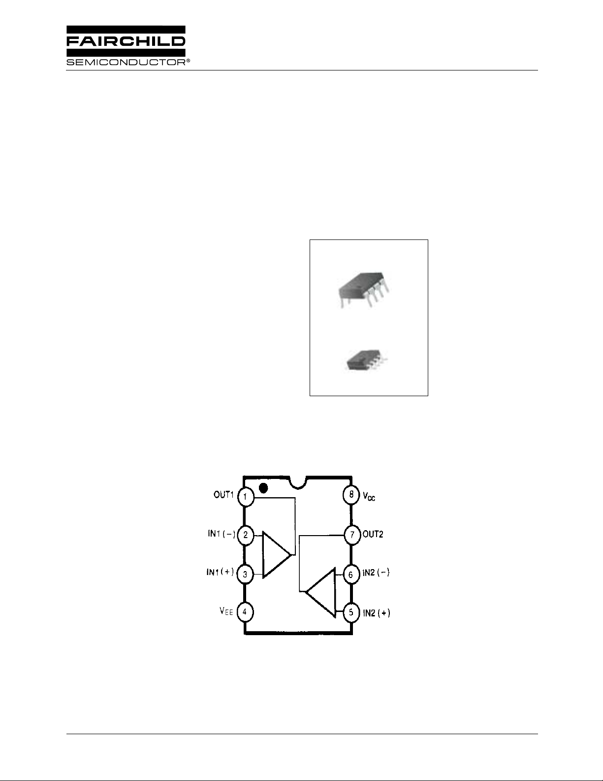
Internal Block Diagram
Description
The LF353 is a JFET input operational amplifier with an
internally compensated input offset voltage. The JFET input
device provides wide bandwidth, low input bias currents and
offset currents.
8-DIP
1
8-SOP
1
©2001 Fairchild Semiconductor Corporation
Rev. 1.0.0
Page 2
LF353
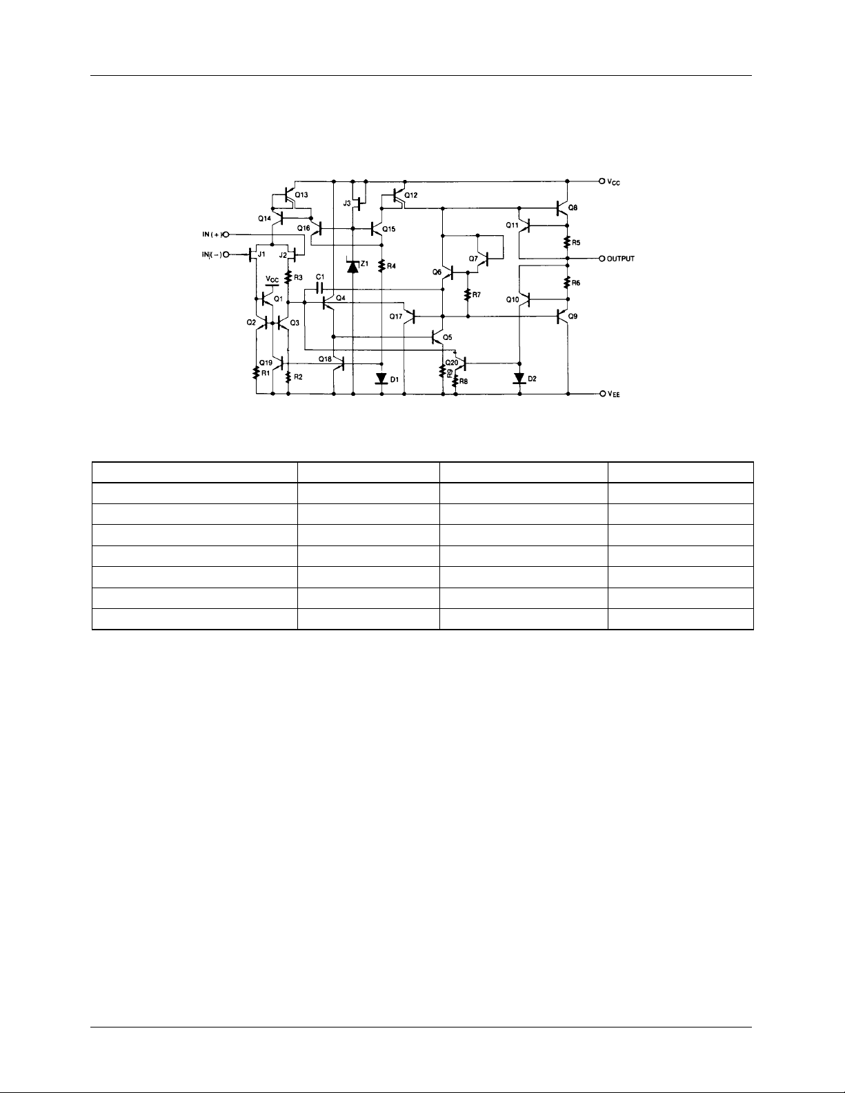
Schematic Diagram
(One Section Only)
Absolute Maximum Ratings
Parameter Symbol Value Unit
Power Supply Voltage V
Differential Input Voltage V
I(DIFF)
Input Voltage Range V
CC
I
±18 V
30 V
±15 V
Output Short Circuit Duration - Continuous Power Dissipation P
Operating Temperature Range T
Storage Temperature Range T
D
OPR
STG
500 mW
0 ~ +70 °C
-65 ~ +150 °C
2
Page 3

LF353
Electrical Characteristics
(V
=+15V, VEE= -15V, TA=25
CC
Parameter Symbol Conditions Min. Typ. Max. Unit
Input Offset Voltage V
Input Offset Voltage Drift ∆V
Input Offset Current I
Input Bias Current I
Input Resistance R
Large Signal Voltage Gain G
Output Voltage Swing V
Input Voltage Range V
Common Mode Rejection Ratio CMRR R
Power Supply Rejection Ratio PSRR R
Power Supply Current I
Slew Rate SR G
Gain-Bandwidth Product GBW - -4-MHz
Channel Seperation CS
Equivalent Input Noise Voltage V
Equivalent Input Noise Current I
°C, unless otherwise specified)
RS=10KΩ -5.010mV
IO
/∆T RS=10KΩ 0
IO
IO
BIAS
I
V
V
O(P_P)RL
I(R)
CC
O(P-P)
R
= 2KΩ 0
L
= 10KΩ±12 ±13.5 - V
≤ 10KΩ 70 100 - dB
S
≤ 10KΩ 70 100 - dB
S
= 1 - 13 - V/µS
V
0
0
0
- -10
= ±10V 25 100 - V/mV
- ±11 ±15/-12 - V
--3.66.5mA
f = 1Hz ~ 20KHz
(Input referenced)
RS = 100Ω
NI
f = 1KHz
f = 1KHz - 0.01 -
NI
°C≤TA≤+70 °C- - - -
°C≤TA≤+70 °C- 10 - µV/ °C
- 25 100 pA
°C≤TA≤+70 °C- - 4 nA
- 50 200 pA
°C≤TA≤+70 °C- - 8 nA
12
°C≤TA≤+70 °C15 - - -
- Ω
- 120 - dB
-16-
nV/
Hz
pA/
Hz
3
Page 4
LF353
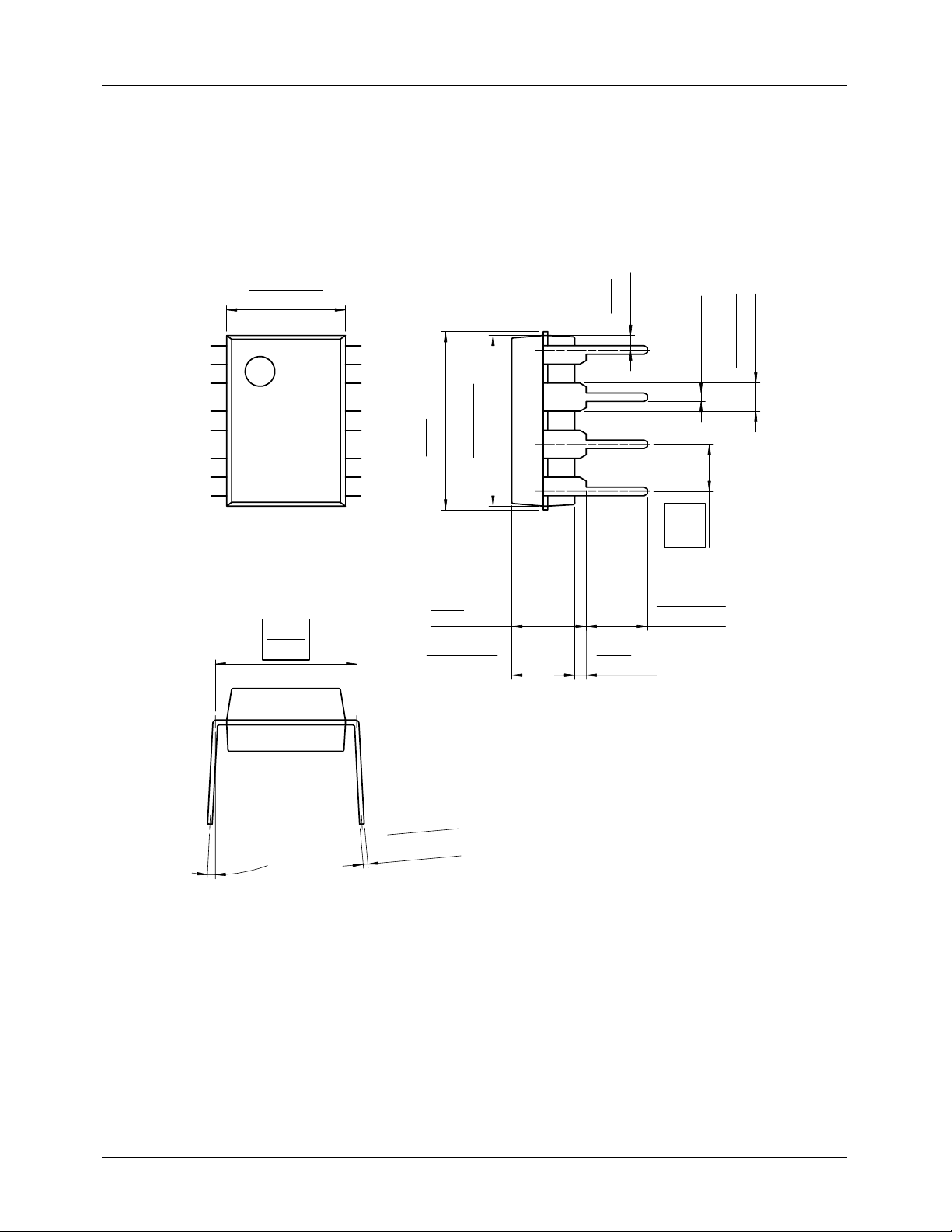
Mechanical Dimensions
Package
6.40 ±0.20
0.252
±0.008
8-DIP
0.79
0.031
()
±0.10
#1
#4 #5
7.62
0.300
#8
MAX
9.60
9.20 ±0.20
0.378
5.08
MAX
0.200
3.40 ±0.20
0.134 ±0.008
0.362 ±0.008
0.33
0.013
3.30 ±0.30
0.130 ±0.012
MIN
0.46
2.54
0.018 ±0.004
0.100
1.524 ±0.10
0.060 ±0.004
+0.10
0.25
–0.05
+0.004
0.010
–0.002
0~15°
4
Page 5

Mechanical Dimensions
Package
8-SOP
1.55
0.061
±0.20
±0.008
0.1~0.25
MIN
0.004~0.001
0.56
0.022
()
LF353
0.006
-0.002
0.50
0.020
+
0.004
±0.20
±0.008
0.15
-0.05
+
0.10
#1
#4
6.00
0.236
3.95
0.156
5.72
0.225
±0.30
±0.012
±0.20
±0.008
#8
#5
5.13
1.80
0.071
0~8°
MAX
0.202
±0.20
4.92
MAX
±0.008
0.194
MAX0.10
MAX0.004
1.27
0.050
±0.004
±0.10
0.41
0.016
5
Page 6

LF353
Ordering Information
Product Number Package Operating Temperature
LF353N 8-DIP
LF353M 8-SOP
0 ~ + 70°C
DISCLAIMER
FAIRCHILD SEMICONDUCTOR RESERVES THE RIGHT TO MAKE CHANGES WITHOUT FURT HER NOTICE TO ANY
PRODUCTS HEREI N TO IMPROVE RELIABILITY, FUNCTIO N OR DESIGN. FAIRCH IL D DOES NOT ASSUME ANY
LIABILITY ARISING OUT OF THE APPLICATION OR USE OF ANY PRODUCT OR CIRCUIT DESCRIBED HEREIN; NEITHER
DOES IT CONVEY ANY LICENSE UNDER IT S PATENT RIGHTS, NOR THE RIGHTS OF OTHE RS.
LIFE SUPPORT POL I CY
FAIRCHILD’S PR ODUCTS ARE NOT AUTH ORIZED FOR USE AS C RITICAL COMPONENT S IN LIFE SUPPORT DE VICES
OR SYSTEMS WITHOUT THE EXPRESS WRITTEN APPROVAL OF THE PRESIDENT OF FAIRCHILD SEMICONDUCTOR
CORPORATION. As used herein :
1. Life support devices or systems are devices or systems
which, (a) are intended for surgical implant into the body,
or (b) support or sustain life, and (c) whose failure to
perform when properly used in accordance with
2. A critical component in any component of a life support
device or sy stem whose fai lure to perform can be
reasonably expec ted to cause the failur e of the life support
device or system, or to affect its safety or effec t iv ene ss .
instructions for use provided in the labeling, can be
reasonably expected to result in a significant injury of the
user.
www.fairchildsemi.com
6/1/01 0.0m 001
2001 Fairchild Semiconductor Corporation
Stock#DSxxxxxxxx
 Loading...