

SGS Thomson Microelectronics LD1117BS33TR, LD1117BS28TR, LD1117BS25TR, LD1117BS18TR, LD1117BDT50TR Datasheet
...
LD1117A/B
SERIES
LOW DROP FIXED AND ADJUSTABLE
POSITIVE VOLTAGE REGULATORS
PRELIMINARY DATA
June 2000
BLOCKDIAGRAM
TO-252 (DPAK)SOT-223
■ LOWDROPOUT VOLTAGE
(1.15VTYP@ I
OUT
=1.2A,25oC)
■
VERYLOW QUIESCENTCURRENT
(5mA TYP @ 25
o
C)
■ TYPEA: OUTPUTCURRENT UPTO 1000mA
■
TYPEB: OUTPUTCURRENT UPTO 1200mA
■ FIXED OUTPUTVOLTAGE OF:1.8V, 2.5V,
2.85V, 3.3V,5.0V
■
ADJUSTABLEVERSIONAVAILABILITY
(V
ref
=1.25V)
■ INTERNALCURRENTAND THERMALLIMIT
■
ONLY10µF FOR STABILITY
■ AVAILABLEIN± 2% (AT 25
o
C) AND4% IN
FULLTEMPERATURERANGE
■
HIGHSUPPLY VOLTAGEREJECTION:
(80dBTYP)
■ TEMPERATURERANGE: 0
o
C TO 125oC
DESCRIPTION
The LD1117A and LD1117B are two LOW
DROP Voltage Regulator able to provide
respectively up to 1000mA and 1200mA of
Output Current, available even in adjustable
version (V
ref
=1.25V). Concerning fixed versions,
are offered the following Output Voltages: 1.8V,
2.5V, 2.85V, 3.3V and 5.0V. The 2.85V type is
ideal for SCSI-2 lines active termination. The
device is supplied in: SOT-223, DPAK. The
SOT-223 and DPAK surface mount packages
optimize the thermal characteristics even
offering a relevant space saving effect. High
efficency is assured by NPN pass transistor. In
fact in this case, unlike than PNP one, the
Quiescent Current flows mostly into the load.
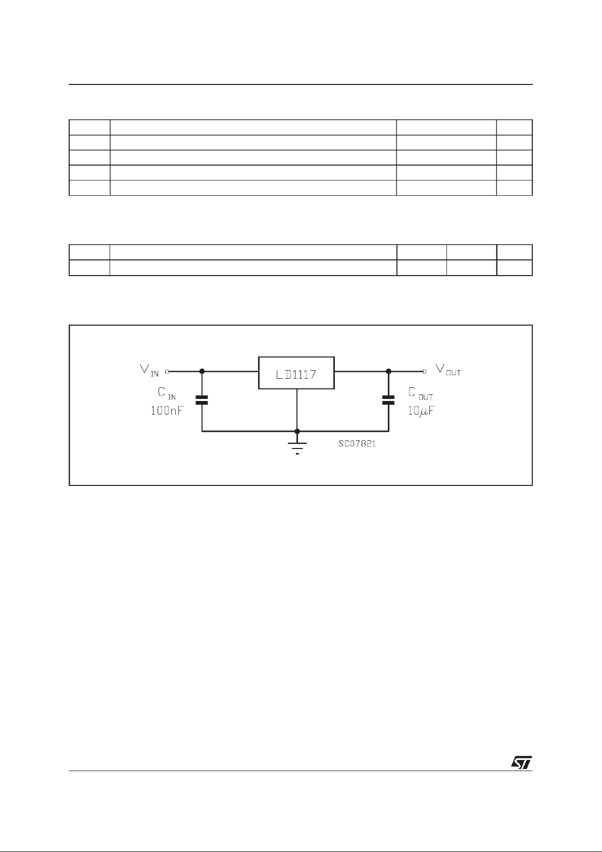
Only a very common 10µF minimum capacitor
is needed for stability. The ADJUSTABLE
LD1117 is pin to pin compatible with the other
standard Adjustable voltage regulators
maintaining the better performances in terms of
Drop and Tolerance.
1/16
ABSOLUTE MAXIMUM RATINGS
Symbol Parameter Value Unit
V
IN
DC InputVoltage 10 V
P
tot
PowerDissipation 12 W
T
stg
Storage TemperatureRange -40 to 150
o
C
T
op
OperatingJunction TemperatureRange 0 to 125
o
C
Absolute Maximum Ratings are those value beyond which damage to the device may occur. Functional operation under these condition is
not implied. Over the above suggested Max PowerDissipation a ShortCircuit could definetively damage the device.
THERMALDATA
Symbol Parameter SOT-223 DPAK Unit
R
thj-cas e
Thermal Resistance Junction-case 15 8
o
C/W
APPLICATION CIRCUIT
LD1117A/B SERIES
2/16
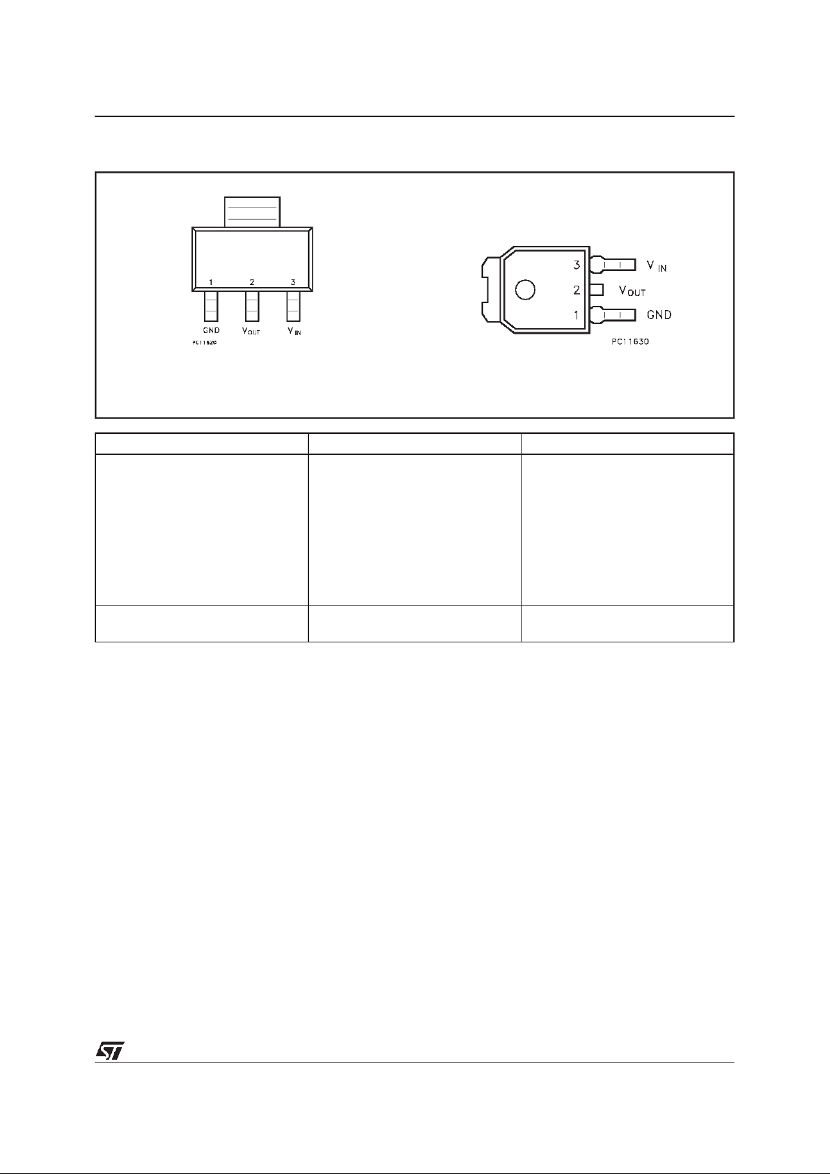
CONNECTION DIAGRAM AND ORDERING NUMBERS
(top view)
SOT-223 DPAK OutputVoltage
LD1117AS18TR
LD1117BS18TR
LD1117AS25TR
LD1117BS25TR
LD1117AS28TR
LD1117BS28TR
LD1117AS33TR
LD1117BS33TR
LD1117AS50TR
LD1117BS50TR
LD1117ADT18TR
LD1117BDT18TR
LD1117ADT25TR
LD1117BDT25TR
LD1117ADT28TR
LD1117BDT28TR
LD1117ADT33TR
LD1117BDT33TR
LD1117ADT50TR
LD1117BDT50TR
1.8V
1.8V
2.5V
2.5V
2.85V
2.85V
3.3V
3.3V
5V
5V
LD1117AST-R
LD1117BST-R
LD1117ADT-R
LD1117BDT-R
ADJUSTABLE
FROM 1.25 TO 15V
SOT-223 DPAK
LD1117A/B SERIES
3/16
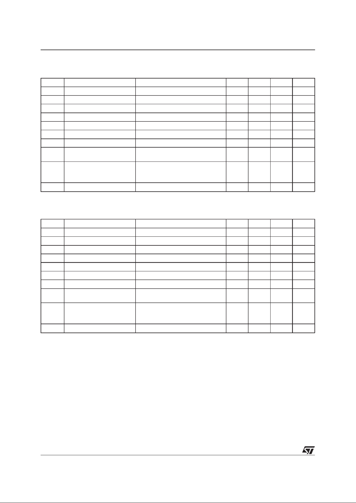
ELECTRICAL CHARACTERISTICS FOR LD1117A#18
(refer to the test circuits,
T
j
= 0 to 125oC, CO=10µF, CI=10µF unless otherwise specified)
Symbol Parameter Test Conditions Min. Typ. Max. Unit
V
O
OutputVoltage VI=3.8 V IO=10mA Tj=25oC 1.764 1. 8 1.836 V
V
O
OutputVoltage IO= 0 to1000mA VI= 3.3to 8 V 1.728 1.872 V
∆
V
O
LineRegulation VI=3.3 to 8 V IO=0 mA 1 6 mV
∆
V
O
LoadRegulation VI=3.3 V IO= 0 to 1000mA 1 10 mV
V
I
OperatingInput Voltage IO= 100mA 10 V
I
d
QuiescentCurrent V
I
≤
8V I
O
=0 mA 5 10 mA
I
O
OutputCurrent VI-VO=5V Tj=25oC 1000 1200 mA
SVR Supply VoltageRejection I
O
= 40 mA f = 120 Hz
V
I-VO
=3V V
ripple
= 1 Vpp
60 80 dB
V
D
Dropout Voltage IO= 100mA
I
O
= 500mA
I
O
= 1000 mA
1
1.05
1.15
1.10
1.15
1.30
V
V
V
∆
V
O(pw r)
Thermal Regulation Ta=25oC 30msPulse 0.08 0.2 %/W
ELECTRICAL CHARACTERISTICS FOR LD1117B#18(refer to the test circuits,
T
j
= 0 to 125oC, CO=10µF, CI=10µF unless otherwise specified)
Symbol Parameter Test Conditions Min. Typ. Max. Unit
V
O
OutputVoltage VI=3.8 V IO=10mA Tj=25oC 1.764 1. 8 1.836 V
V
O
OutputVoltage IO= 0 to1200mA VI= 3.3to 8 V 1.728 1.872 V
∆V
O
LineRegulation VI=3.3 to 8 V IO=0 mA 1 6 mV
∆V
O
LoadRegulation VI=3.3 V IO= 0 to 1200mA 1 10 mV
V
I
OperatingInput Voltage IO= 100mA 10 V
I
d
QuiescentCurrent V
I
≤
8V I
O
=0 mA 5 10 mA
I
O
OutputCurrent VI-VO=5V Tj=25oC 1200 1500 mA
SVR Supply VoltageRejection I
O
= 40 mA f = 120 Hz
V
I-VO
=3V V
ripple
= 1 Vpp
60 80 dB
V
D
Dropout Voltage IO= 100mA
I
O
= 500mA
I
O
= 1200 mA
1
1.05
1.15
1.10
1.15
1.30
V
V
V
∆V
O(pw r)
Thermal Regulation Ta=25oC 30msPulse 0.08 0.2 %/W
LD1117A/B SERIES
4/16
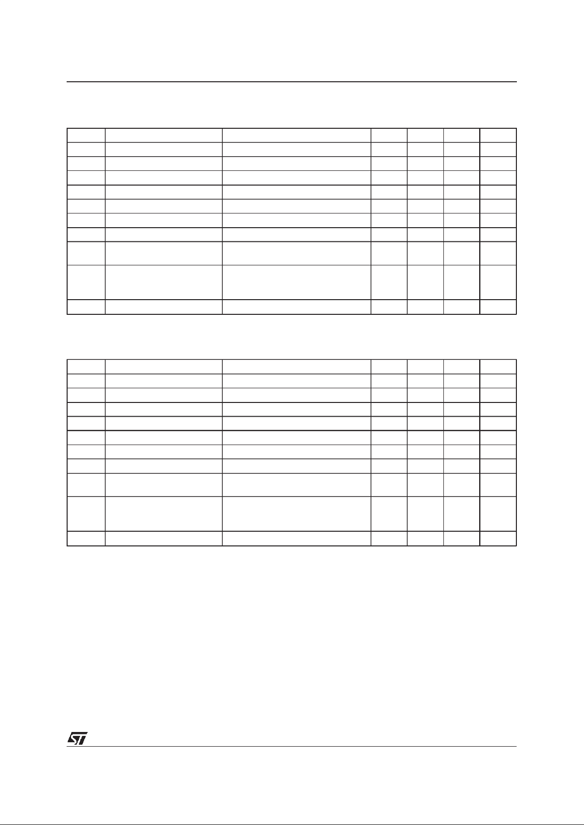
ELECTRICAL CHARACTERISTICS FOR LD1117A#25
(refer to the test circuits,
T
j
= 0 to 125oC, CO=10µF, CI=10µF unless otherwise specified)
Symbol Parameter Test Conditions Min. Typ. Max. Unit
V
O
OutputVoltage VI=4.5 V IO=10mA Tj=25oC 2.45 2.5 2.55 V
V
O
OutputVoltage IO= 0 to1000mA VI= 3.9to 8 V 2.4 2.6 V
∆
V
O
LineRegulation VI=3.9 to 8 V IO=0 mA 1 6 mV
∆
V
O
LoadRegulation VI=3.9 V IO= 0 to 1000mA 1 10 mV
V
I
OperatingInput Voltage IO= 100mA 10 V
I
d
QuiescentCurrent V
I
≤
10 V I
O
=0 mA 5 10 mA
I
O
OutputCurrent VI-VO=5V Tj=25oC 1000 1200 mA
SVR Supply VoltageRejection I
O
= 40 mA f = 120 Hz
V
I-VO
=3V V
ripple
= 1 Vpp
60 80 dB
V
D
Dropout Voltage IO= 100mA
I
O
= 500mA
I
O
= 1000 mA
1
1.05
1.15
1.10
1.15
1.30
V
V
V
∆
V
O(pw r)
Thermal Regulation Ta=25oC 30msPulse 0.08 0.2 %/W
ELECTRICAL CHARACTERISTICS FOR LD1117B#25(refer to the test circuits,
T
j
= 0 to 125oC, CO=10µF, CI=10µF unless otherwise specified)
Symbol Parameter Test Conditions Min. Typ. Max. Unit
V
O
OutputVoltage VI=4.5 V IO=10mA Tj=25oC 2.45 2.5 2.55 V
V
O
OutputVoltage IO= 0 to1200mA VI= 3.9to 8 V 2.4 2.6 V
∆V
O
LineRegulation VI=3.9 to 8 V IO=0 mA 1 6 mV
∆V
O
LoadRegulation VI=3.9 V IO= 0 to 1200mA 1 10 mV
V
I
OperatingInput Voltage IO= 100mA 10 V
I
d
QuiescentCurrent V
I
≤
10 V I
O
=0 mA 5 10 mA
I
O
OutputCurrent VI-VO=5V Tj=25oC 1200 1500 mA
SVR Supply VoltageRejection I
O
= 40 mA f = 120 Hz
V
I-VO
=3V V
ripple
= 1 Vpp
60 80 dB
V
D
Dropout Voltage IO= 100mA
I
O
= 500mA
I
O
= 1200 mA
1
1.05
1.15
1.10
1.15
1.30
V
V
V
∆V
O(pw r)
Thermal Regulation Ta=25oC 30msPulse 0.08 0.2 %/W
LD1117A/B SERIES
5/16
 Loading...