

L9820
HIGH SIDE DRIVER
ADVANCE DATA
OPERATINGSUPPLYVOLTAGE UP TO25V
DC CURRENT 0.3A
< 800mΩ
R
ON
DIAGNOSTIC AND PROTECTION FUNCTIONS
µP COMPATIBLE
ENABLEINPUT FOR STAND-BY MODE
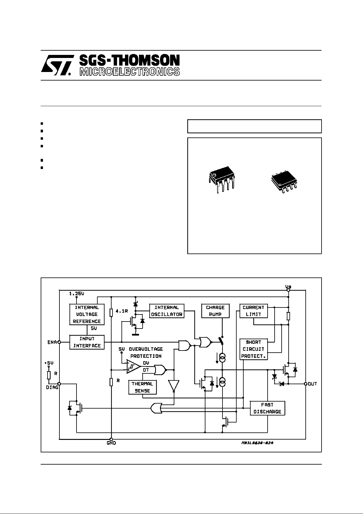
DESCRIPTION
The L9820 High Side Driver realized with Multipower - BCD mixed technology, drives resistive
or inductive loads with one side connected to
ground.
The ENABLEinput is TTL compatibleand a diagnostic outputprovides an indicationof short circuit
and device status (thermal and overvoltage shutdown).Onchip thermal protection and short circuit
protectionare provided.
BLOCKDIAGRAM
MULTIPOWER BCD TECHNOLOGY
Minidip SO8
ORDERING NUMBERS:
L9820 L9820D
40mΩ
February 1994
This is advanced information on anew product now in development or undergoing evaluation. Details are subject to change without notice.
1/6
L9820
ABSOLUTE MAXIMUM RATINGS
Symbol Parameter Value Unit
V
S
I
R
V
5
V
8
V
1
I
4
I
5
I
8
I
1
T
op
T
j,Tstg
T
jp
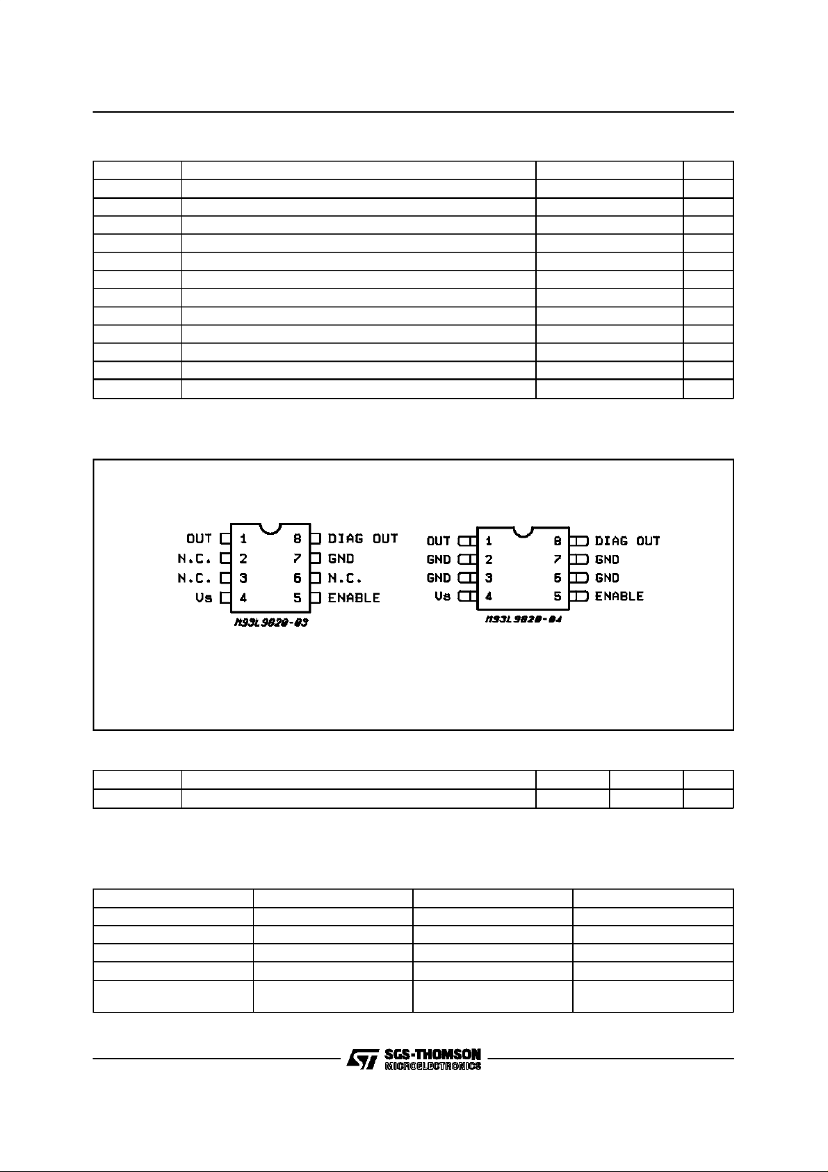
PIN CONNECTION (Topviews)
Max Forward Voltage 50 Vdc
Reverse Bias Current at -1.3V –0.46 A
Input Voltage (to GND) –0.3 to 20 V
Diag. OutputVoltage (toGND) –0.3 to 20 V
Output Voltage (to GND) –0.3 to 25 V
Supply Current Internally limited
Enable Input Current 0.5 mA
Diag. Out Current (sink) 10 mA
Output Current Internally limited
Operation Temperature –40 to 85 °C
Junction and Storage Temperature Range –55 to 150 °C
Detecting Temperature 150 °C
Minidip
SO8
THERMALDATA
Symbol Parameter Minidip SO8 Unit
R
th j-amb
Thermal Resistance Junction-ambient Max. 100 200 °C/W
TRUTHTABLE
H: high level
L:low level
ENABLE FUNCTION DIAG. STATUS POWER STATUS
L Operating OFF H L
H Normal Operation H H
H Overvoltage Protection ON L L
H Overcurrent Protection ON L L
H Overtemperature
Protection ON
2/6
LL

PIN FUNCTIONS
N. Name Description
1 POWER OUTPUT The deviceis provided with short circuit protection.
4 POWERSUPPLY Supply voltage input.
5 ENABLE INPUT TTL compatible input. High level on thispin meansoutput current ON.
Thelow level voltage switches off the charge pump, the power stage and
thediagnostic outputreducing to the minimum value thequiescent current.
7 GROUND This pin must be connected to ground.
8 DIAGNOSTIC FEEDBACK The diagnostic circuit is active in input high level condition. This output
detects with Tipically 50µs delay at T
=25°C the following faults:
amb
– Overvoltagecondition.
– Thermal shutdown.
– Shortcircuit. The power stage current is internally limited at 1.5A.
Thediagnostic output is active low. The diagnostic delay timeallows to
avoid spurious diagnosys(i.e.: turnON overcurrent, overvoltage spikes etc.).
ELECTRICAL CHARACTERISTICS (VS=14.4V, –40°C≤ Tj≤ +85°C, unless otherwisespecified.)
Symbol Parameter Test Condition Min. Typ. Max. Unit
V
S
R
on
I
off
I
on
V
EL
V
EH
I
E
I
leakd
V
satd
t
dd
t
don
t
r
t
doff
t
f
V
don
V
dh
I
don
T
don
T
dh
Operating Supply Voltage 6 25 V
On Resistance Input> 2V,Tj=25°C
Input> 2V,Full T range
Off State Supply Current Tj<35°C
T
=85°C
j
0.6 0.8
1.2
130
300
On State Supply Current 4 mA
Enable Low Level 0.8 V
Enable HighLevel 2 V
Enable Current 0V < Vi <5V 10 µA
Diagnostic Outp ut Leakage Current VCC= 5V Diagnostic OutputHigh 10 µA
Diagnostic Output Saturated
Isink < 3.5mA 0.4 V
Voltage
Diagnostic Delay Time Tj=25°C30µs
Output ON Delay Time Tj=25°C30µs
Output ON Rise Time Tj = 25°C 100 µs
Output OFF Delay Time Tj= 25°C80µs
Output OFF Fall Time Tj = 25°C 100 µs
Overvoltage Detection ON 25 V
Overvoltage Hysteresis 2 5 V
Overcurrent Detection ON 0.5 1.5 A
Overtemperature Detection ON 150 °C
Overtemperature Hysteresis 25 50 °C
L9820
Ω
Ω
µA
µA
3/6

L9820
SO8 PACKAGEMECHANICAL DATA
DIM.
A 1.75 0.069
a1 0.1 0.25 0.004 0.010
a2 1.65 0.065
a3 0.65 0.85 0.026 0.033
b 0.35 0.48 0.014 0.019
b1 0.19 0.25 0.007 0.010
C 0.25 0.5 0.010 0.020
c1 45 1.772
D 1 4.8 0.039 0.189
E 5.8 6.2 0.228 0.244
e 1.27 0.050
e3 3.81 0.150
F 1 3.8 0.039 0.150
G
L 0.4 1.27 0.016 0.050
M 0.6 0.024
S 8 0.315
MIN TYP MAX MIN TYP MAX
mm inch
4/6

MINIDIPPACKAGE MECHANICAL DATA
L9820
DIM.
MIN. TYP. MAX. MIN. TYP. MAX.
A 3.32 0.131
a1 0.51 0.020
B 1.15 1.65 0.045 0.065
b 0.356 0.55 0.014 0.022
b1 0.204 0.304 0.008 0.012
D 10.92 0.430
E 7.95 9.75 0.313 0.384
e 2.54 0.100
e3 7.62 0.300
e4 7.62 0.300
F 6.6 0.260
I 5.08 0.200
L 3.18 3.81 0.125 0.150
mm inch
Z 1.52 0.060
5/6

L9820
Information furnished is believed to be accurate and reliable. However, SGS-THOMSON Microelectronics assumes no responsibility for the
consequences of use of such information nor for any infringement of patents or other rights of third parties which may result from its use. No
license is granted by implication or otherwise under any patent or patentrights of SGS-THOMSON Microelectronics. Specification mentioned
in this publication are subject to change without notice. This publication supersedes and replaces all information previously supplied.
SGS-THOMSON Microelectronics products arenot authorized for use as critical componentsin life support devices orsystems without express
written approval of SGS-THOMSON Microelectronics.
1996 SGS-THOMSON Microelectronics – Printed in Italy – All Rights Reserved
SGS-THOMSON Microelectronics GROUP OF COMPANIES
Australia - Brazil - Canada - China - France - Germany - Hong Kong - Italy - Japan - Korea - Malaysia - Malta - Morocco - The Netherlands -
Singapore- Spain - Sweden - Switzerland - Taiwan - Thailand - United Kingdom - U.S.A.
6/6
 Loading...