

SGS Thomson Microelectronics L79L15CD, L79L15ACZ, L79L15ACU, L79L12CD, L79L12ACZ Datasheet
...
L79L00
SERIES
NEGATIVEVOLTAGE REGULATORS
December 1999
■ OUTPUT CURRENT UP TO100 mA
■
OUTPUT VOLTAGESOF-5;-6; -8; -9; -12;
-15V
■
THERMAL OVERLOADPROTECTION
■ SHORTCIRCUITPROTECTION
■ NOEXTERNALCOMPONENTS ARE
REQUIRED
■ AVAILABLEIN EITHER± 5% (AC)OR ± 10%
(C)SELECTION
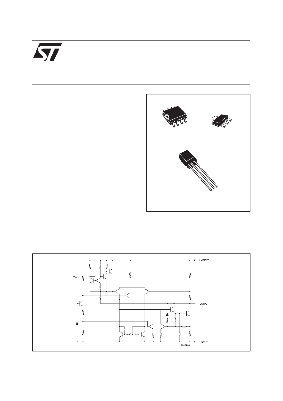
DESCRIPTION
The L79L00 series of three-terminal positive
regulators employ internal current limiting and
thermal shutdown, making them essentially
indestructible. If adequate heatsink is provided,
they can deliver up to 100 mA output current.
They are intended as fixedvoltage regulators in a
wide range of applications including local or
on-card regulation for elimination of noise and
distribution problems associated with single-point
regulation. In addition, they can be used with
power pass elements to make high-current
voltageregulators.
The L79L00 series used as Zener diode/resistor
combination replacement, offers an effective
BLOCKDIAGRAM
SO-8
TO-92
output impedance improvement of typically two
orders of magnetude, along with lower quiescent
currentand lower noise.
SOT-89
1/13
ABSOLUTE MAXIMUM RATING
Symbol Parameter Value Unit
V
i
DC InputVoltage Vo= -5 V to-9 V -30 V
V
o
= -12V to -15 V -35 V
I
o
OutputCurrent 100 mA
P
tot
PowerDissipation Internally limited (*)
T
stg
StorageTemperature Range - 40 to 150
o
C
T
op
OperatingJunctionTemperatureRange For L79L00C, L79L00AC
For L79L00AB
0to125
-40to125
o
C
o
C
(*) Our SO-8 package used for Voltage Regulators is modified internally to have pins 2, 3, 6 and 7 electrically commoned to the die attach
flag. This particular frame decreases the total thermal resistance of the package and increases its ability to dissipate power when an
appropriatearea of copper on the printed circuit board is available for heatsinking. The externaldimensions are the same as forthe standard
SO-8
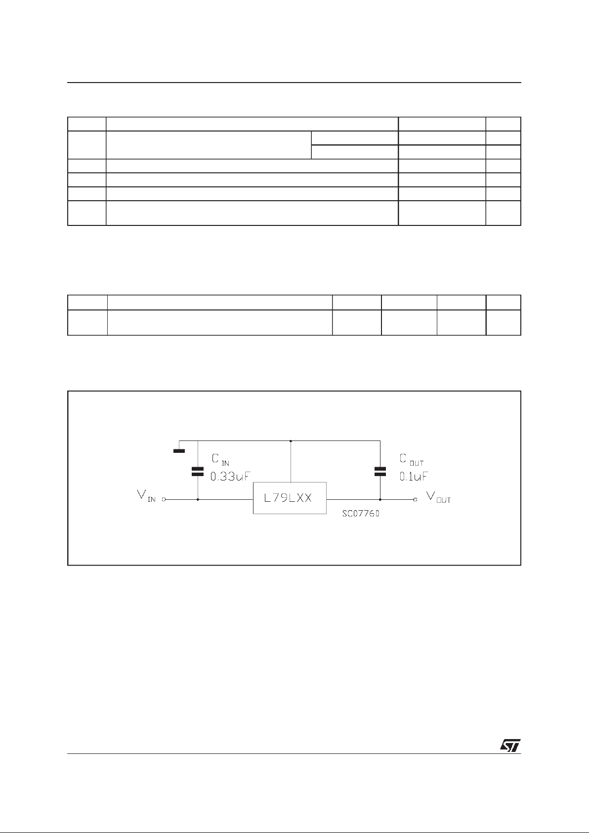
TESTCIRCUITS
THERMALDATA
Symbol Parameter SO-8 TO-92 SOT-89 Unit
R
thj-cas e
R
thj-amb
Thermal Resistance Junction-case Max
Thermal Resistance Junction-ambient Max2055 (*) 200
15
o
C/W
o
C/W
(*) Considering 6cm2of copper Board heat-sink
L79L00
2/13
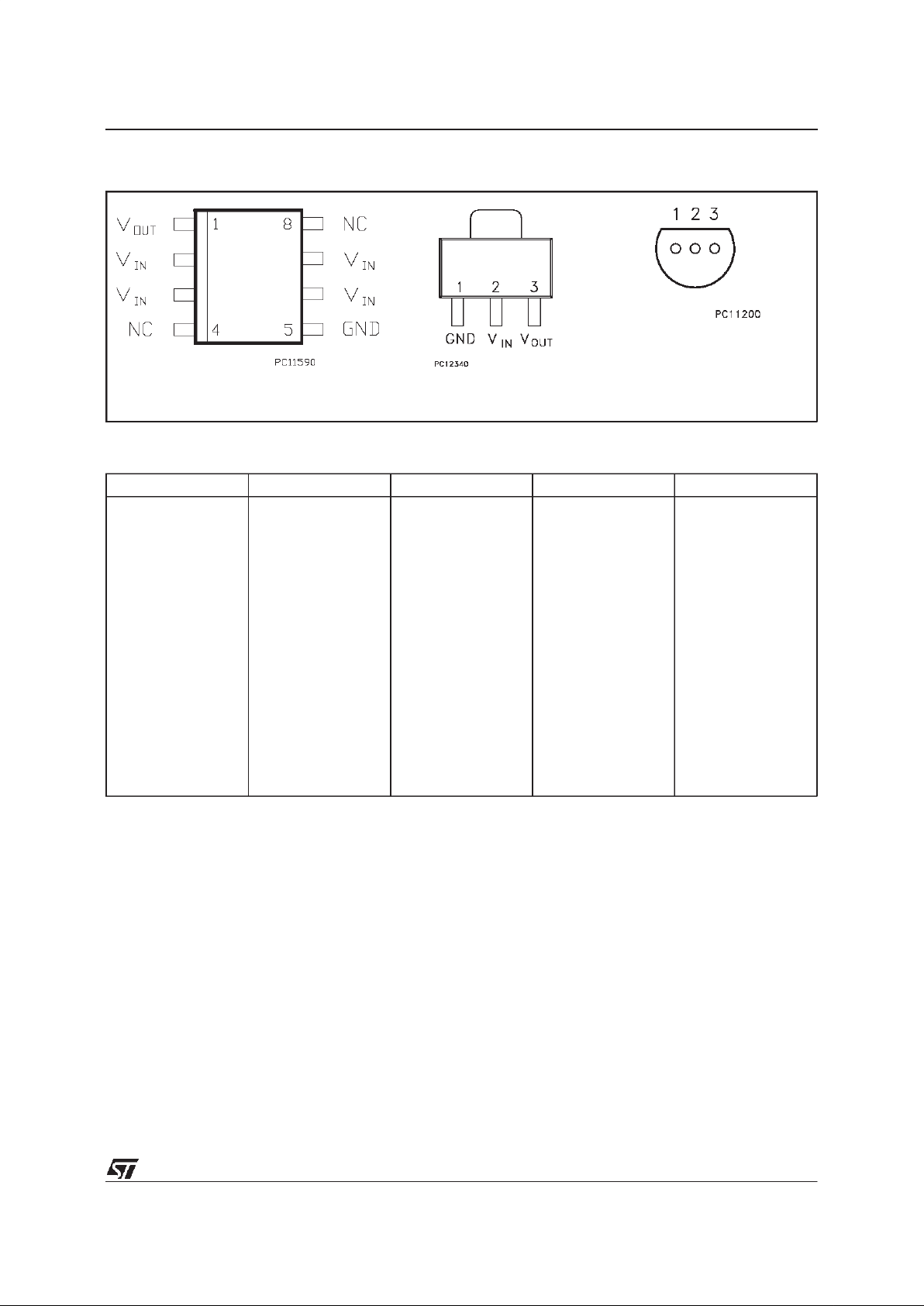
CONNECTION DIAGRAM AND ORDERING NUMBERS
(top view)
ORDERING NUMBERS
Type SO-8 TO-92 SOT-89 Output Voltage
L79L05C
L79L05AC
L79L05AB
L79L06C
L79L06AC
L79L06AB
L79L08C
L79L08AC
L79L08AB
L79L09C
L79L09AC
L79L09AB
L79L12C
L79L12AC
L79L12AB
L79L15C
L79L15AC
L79L15AB
L79L05CD
L79L05ACD
L79L05ABD
L79L06CD
L79L06ACD
L79L06ABD
L79L08CD
L79L08ACD
L79L08ABD
L79L09CD
L79L09ACD
L79L09ABD
L79L12CD
L79L12ACD
L79L12ABD
L79L15CD
L79L15ACD
L79L15ABD
L79L05CZ
L79L05ACZ
L79L05ABZ
L79L06CZ
L79L06ACZ
L79L06ABZ
L79L08CZ
L79L08ACZ
L79L08ABZ
L79L09CZ
L79L09ACZ
L79L09ABZ
L79L12CZ
L79L12ACZ
L79L12ABZ
L79L15CZ
L79L15ACZ
L79L15ABZ
L79L05ACU
L79L05ABU
L79L06ACU
L79L06ABU
L79L08ACU
L79L08ABU
L79L09ACU
L79L09ABU
L79L12ACU
L79L12ABU
-5 V
-5 V
-5 V
-6 V
-6 V
-6 V
-8 V
-8 V
-8 V
-9 V
-9 V
-9 V
-12 V
-12 V
-12 V
-15 V
-15 V
-15 V
SO-8 TO-92
pin 1 = GND
pin 2 = V
IN
pin 3 = V
OUT
BOTTOM VIEW
SOT-89
L79L00
3/13
ELECTRICAL CHARACTERISTICS FOR L79L05
(refer to the test circuits,T
j
= 0 to 125oC,
V
i
= -10V, Io= 40 mA, Ci= 0.33 µF, Co= 0.1µF unless otherwisespecified)
Symbol Parameter Test Conditions Min. Typ. Max. Unit
V
o
OutputVoltage Tj=25oC-4.6-5-5.4V
V
o
OutputVoltage Io=1 to40 mA Vi= -7 to-20 V
I
o
=1 to70 mA Vi= -10 V
-4.5
-4.5
-5.5
-5.5
V
V
∆
V
o
LineRegulation Vi=-7to-20V Tj=25oC
V
i
=-8to-20V Tj=25oC
200
150
mV
mV
∆V
o
LoadRegulation Io=1 to100 mA Tj=25oC
I
o
=1 to40 mA Tj=25oC
60
30
mV
mV
I
d
QuiescentCurrent Tj=25oC
T
j
= 125oC
6
5.5
mA
mA
∆I
d
QuiescentCurrentChange Io=1 to40 mA 0.2 mA
∆I
d
QuiescentCurrentChange Vi=-8to-20V 1.5 mA
eN OutputNoiseVoltage B = 10Hzto 100KHz T
j
=25oC40
µV
SVR Supply VoltageRejection I
o
=40 mA f = 120Hz Tj=25oC
V
i
=-8to-18V
40 49 dB
V
d
Dropout Voltage 1.7 V
ELECTRICAL CHARACTERISTICS FOR L79L06(referto the test circuits,Tj= 0 to 125oC,
V
i
= -12V, Io= 40 mA, Ci= 0.33 µF, Co= 0.1µF unless otherwisespecified)
Symbol Parameter Test Conditions Min. Typ. Max. Unit
V
o
OutputVoltage Tj=25oC -5.52 -6 -6.48 V
V
o
OutputVoltage Io=1 to40 mA Vi= -8.5 to-20 V
I
o
=1 to70 mA Vi= -12 V
-5.4
-5.4
-6.6
-6.6
V
V
∆V
o
LineRegulation Vi= -8.5to -20 V Tj=25oC
V
i
=-9to-20V Tj=25oC
200
150
mV
mV
∆
V
o
LoadRegulation Io=1 to100 mA Tj=25oC
I
o
=1 to40 mA Tj=25oC
60
30
mV
mV
I
d
QuiescentCurrent Tj=25oC
T
j
= 125oC
6
5.5
mA
mA
∆
I
d
QuiescentCurrentChange Io=1 to40 mA 0.2 mA
∆
I
d
QuiescentCurrentChange Vi=-8to-20V 1.5 mA
eN OutputNoiseVoltage B = 10Hzto 100KHz T
j
=25oC50
µ
V
SVR Supply VoltageRejection I
o
=40 mA f = 120Hz Tj=25oC
V
i
=-9to-20V
38 46 dB
V
d
Dropout Voltage 1.7 V
L79L00
4/13
 Loading...