

FOR LOW VOLTAGE OPERATIONS
FEATURES
■ FROM 3V TO 5.5V V
■ MINIM U M O U TPUT VO L T A GE AS LO W AS
0.6V.
■ 1V TO 28V INPUT VOLTAGE RANGE.
■ CONSTANT ON TIME TOPOLOGY ALLO WS .
OPERATION WITH VERYLOW AND HIGH
DUTY CYCLES.
■ VERY FAST LOAD TRANSIENTS.
■ 0.6V, ±1% VREF.
■ SELECTABLE SINKING MODE.
■ LOSSLESS CURRENT LIMIT, AVAILABLE
ALSO IN SINKING MODE
■ REMOTE SENSING.
■ OVP,UVP LATCHED PROTECTIONS.
■ 600µA TYP QUIESCENT CURRENT.
■ POWER GOOD AND OVP SIGNALS.
■ PULSE SKIPPING AT LIGTH LOADS.
■ 94% EFFICIENCY FROM 3.3V TO 2.5V.
APPLICATIONS
■
NETWORKING.
■
DC/DC MODULES.
■
DISTRIBUTED POWER.
■
MOBILE A PPLICATIONS.
■
CHIP SET, CPU, DSP AND MEMORIES SUPPLY.
RANGE.
CC
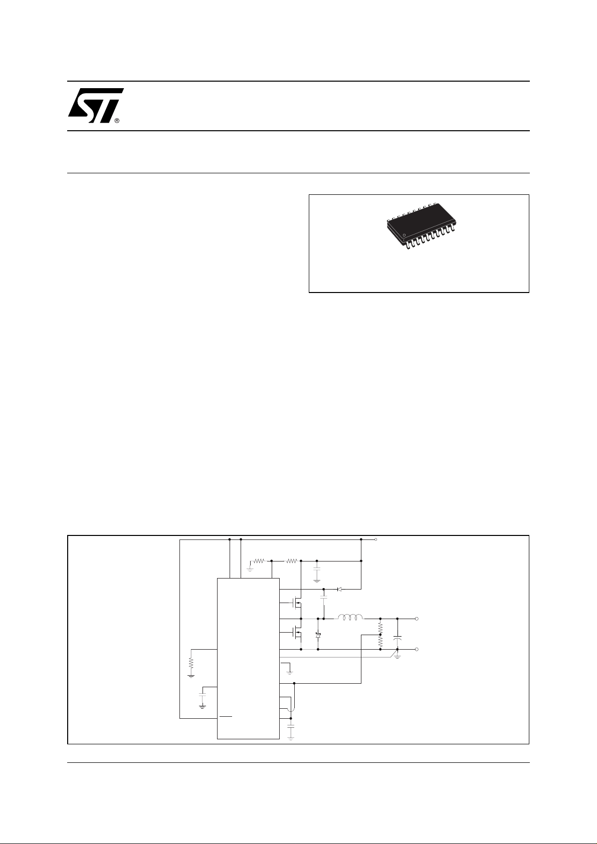
L6997
STEP DOWN CONTROLLER
TSSOP20
ORDERING NUMBERS: L6997D
L6997DTR
DESCRIPTION
The device is a high efficient solution for networking
dc/dc modules and mobile application compatible
with 3.3V bus and 5V bus.
It's able to regulate an output vol tage as low as 0.6V.
The constant on time topology assures fast load tran-
sient response. The embedded voltage feed-forward
provides nearly constant switching frequency operation.
An integrator can be introduced in the control loop to
reduce the static output voltage error.
The remote sensing improv es the static and dynamic
regulation, recovering the wires voltage drop.
Pulse skipping technique reduces power consumption at light loads. Drivers current capability allows
output currents in excess of 20A.
MINIMUM COMPONENT COUNT APPLICATION
VDR
L6997
OSC
BOOT
HGATE
PHASE
LGATE
PGND
GND
GNDSENSE
VSENSE
INT
VFB
Vref
VCC
PGOOD
OVP
ILIM
Rilim
SS
Css
SHDN
April 2003
3.3V
Rin1Rin2
Cin
Dboot
HS
Cboot
Cvref
L
DS
LS
Ro1
Ro2
0.6V
Cout
1/23
L6997
ABSOLUTE MAXIMUM RATINGS
Symbol Parameter Value Unit
V
CC
V
DR
V
PHASE
P
tot
T
stg
THERMAL DATA
Symbol Parameter Value Unit
VCC to GND -0.3 to 6 V
V
to GND -0.3 to 6 V
DR
HGATE and BOOT, to PHASE -0.3 to 6 V
HGATE and BOOT, to PGND -0.3 to 36 V
PHASE -0.3-to 30 V
LGATE to PGND -0.3 to V
ILIM, VFB, VSENSE, NOSKIP, SHDN, PGOOD, OVP, VREF, INT,
SENSE
to GND
= 25°C 1 W
amb
GND
Power dissipation at T
-0.3 to V
+0.3 V
DR
+0.3 V
CC
Storage temperature range -40 to 150 °C
R
th j-amb
PIN CONNECTION
Thermal Resistance Junction to Ambient 125 °C/W
T
Junction operating temperature range -40 to 125 °C
j
(Top View)
NOSKIP
GNDSENSE
INT
INT
VSENSE
VCC
GND
VREF
VFB
OSC
2
3
4
5
6
7
8
9
10SS
TSSOP20
20
BOOT1
19
HGATE
18
PHASE
17
VDR
16
LGATE
15
PGND
14
PGOOD
13
OVP
12
SHDN
11
ILIM
PIN FUNCTION
N° Name Description
1 NOSKIP Connect to V
2 GNDSE
Remote ground sensing pin
NSE
3 INT Integrator output. Short this pin to VFB pin and connect it via a capacitor to V
integrator in the control loop. If the integrator is not used, short this pin to VREF.
4 VSENSEThis pin must be connected to the remote output voltage to detect overvoltage and undervoltage
conditions and to provide integrator feedback input.
5V
IC Supply Voltage.
CC
6 GND Signal ground
7 VREF 0.6V voltage reference. Connect max. a 10nF ceramic capacitor between this pin and ground.
This pin is capable to source or sink up to 250uA
to force continuous conduction mode and sink mode.
CC
to insert the
OUT
2/23
L6997
PIN FUNCTION
(continued)
N° Name Description
8 VFB PWM comparator feedback input. Short this pin to INT pin when using the integrator function, or
to VSENSE pin without integrator.
9 OSC Connect this pin to the input voltage through a voltage divider in order to provide the feed-
forward function. It cannot be left floating.
10 SS Soft start pin. A 5µA constant current charges an external capacitor which value sets the soft-
start time.
11 ILIM An external resistor connected between this pin and GND sets the current limit threshold.
12 SHDN Shutdown. When connected to GND the device and the drivers are OFF. It cannot be left floating.
13 OVP Open drain output. During the over voltage condition it is pulled up by an external resistor.
14 PGOOD Open drain output. During the soft start and in case of output voltage fault it is low. It is pulled up
by external resistor.
15 PGND Low Side driver ground.
16 LGATE Low Side driver output.
17 V
Low Side driver supply.
DR
18 PHASE Return path of the High Side driver.
19 HGATE High side MOSFETS driver output.
20 BOOT Bootstrap capacitor pin. High Side driver is supplied through this pin.
ELECTRICAL CHARACTERISTICS
= VDR = 3.3V; T
(V
CC
= 0°C to 85°C unless otherwise specified)
amb
Symbol Parameter Test Condition Min. Typ. Max. Unit
SUPPLY SECTION
Vin Input voltage range Vout=Vref Fsw=110Khz Iout=1A 1 28 V
V
,
CC
V
DR
V
Turn-onvoltage 2.86 2.97 V
CC
3 5.5 V
Tu r n-off voltage 2.75 2 .9 V
Hysteresis 90 mV
IqV
Quiescent Current Drivers VFB > VREF 7 20 µA
DR
IqVcc Device Quiescent current VFB > VREF 400 600 µA
SHUTDOWN SECTION
SHDN Device On 1.2 V
Device Off 0.6 V
I
SHVDR
I
SHVCC
Drivers shutdown current SHDN to GND 5 µA
Devices shutdown current SHDN to GND 1 15 µA
SOFT START SECTION
I
Soft Start current VSS = 0.4V 4 6 µA
SS
Active Soft start and voltage 300 400 500 mV
CURRENT LIMIT AND ZERO CURRENT COMPARATOR
ILIM input bias current R
Zero Crossing Comparator offset
= 2KΩ to 200KΩ 4.6 5 5.4 µA
ILIM
-2 2 mV
Phase-gnd
DK
Current limit factor 1.6 1.8 2 µA
ILIM
3/23

L6997
ELECTRICAL CHARACTERISTICS
(V
= VDR = 3.3V; T
CC
= 0°C to 85°C unless otherwise specified)
amb
(continued)
Symbol Parameter Test Condition Min. Typ. Max. Unit
ON TIME
Ton On time duration V
REF=VSENSE OSC
V
REF=VSENSE OSC
V
REF=VSENSE OSC
=125mV 720 800 880 ns
=250mV 370 420 470 ns
=500mV 210 240 270 ns
OFF TIME
T
OFFMIN
Minimum off time 600 ns
K
OSC/TOFFMIN
OSC=250mV 0.3 0.33
VOLTAGE REFERENCE
VREF Voltage Accuracy 0µA < I
< 100µA 0.594 0.6 0.606 V
REF
PWM COMPARATOR
Input voltage offset -2 +2 mV
I
Input Bias Current 20 nA
FB
INTEGRATOR
INT Over Voltage Clamp V
INT Under Voltage Clamp V
Integrator Input Offset Voltage
V
SENSE-VREF
I
VSENSE
Input Bias Current 20 nA
= V
SENSE
SENSE
CC
= GND 0.45 0.55 0.65 V
0.62 0.75 0.88 V
-4 -4 mV
GATE DRIVERS
High side rise time V
High side fall time 50 100 ns
Low side rise time V
Low side fall time 50 90 ns
P
UVP/OVP PROTECTIONS
GOOD
=3.3V; C=7nF
DR
HGATE - PHASE from 1 to 3V
=3.3V; C=14nF
DR
LGATE from 1 to 3V
OVP Over voltage threshold with respect to V
REF
118 121 124 %
50 90 ns
50 90 ns
UVP Under voltage threshold 67 70 73 %
PGOOD Upper threshold
(V
SENSE-VREF
)
PGOOD Lower threshold
)
V
PGOOD
(V
SENSE-VREF
V
rising 110 112 116 %
SENSE
V
falling 85 88 91 %
SENSE
I
=2mA 0.2 0.4 V
Sink
4/23
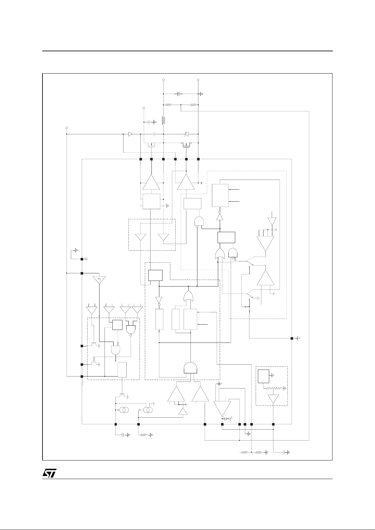
Figure 1. Funct i on a l & Blo c k D iag ram
IN
V
Vcc
L6997
OUT
V
GNDVCCOVPPGOODSHDN
overvoltage comparator
VSENSE
+
1.12 VREF
-+undervoltage comparator
VSENSE
0.6 VREF
pgood comparators
SR
LS and HS anti-cross-conduction comparators
VSENSE
1.075 VREF
-
+
comp
V(LGATE)<0.5V
VSENSE
+
BOOT
VCC
0.925 VREF
-
HGATE
HS driver
level shifter
V(PHASE)<0.2V
Q
R
comp
S
Toff min
PHASE
delay
VDR
Ton min
one-shot
PGND
LGATE
LS driver
Q
R
S
Ton
one-shot
Ton
OSC
VSENSE
Q
S
one-shot
OSC
VSENSE
Ton= Kosc V(VSENSE)/V(OSC)
R
no-skipno-skip
mode
mode
comparator
negative current limit
PHASE
++-
-
+
PHASE
ILIM
0.05
zero-cross comparator
LS control
Ton= Kosc V(VSENSE)/V(OSC)
NOSKIP
IC enable
control
soft-start
SS
5 uA
power management
ILIM
positive current limit
comparator
-
PHASE
+-+
+VREF
0.05
FB
HS control
VREF
pwm comparator
-
-
-
+
+
Gm
VREF
INT
VSENSE
IN
V
SENSEGND
OSC
1.236V
bandgap
VREF
1.416
Reference chain
0.6V
5/23
L6997
1 DEVICE DESCRIPTION
1.1 Constant On Time PWM topology
Figure 2. Loop block schematic diagram
Vin
R1
R2
One-shot generator
OSC
Vsense
Vref
FFSR
Q
R
HGATE
S
Q
+
LGATE
HS
LS
Vout
DS
-
PWM comparator
FB
R4
R3
The device implements a Constant On Time control scheme, where the Ton is the high side MOSFET on time
duration forced by the one-shot generator. The on time is directly proportional to VSENSE pin voltage and inverse to OSC pin voltage as in Eq1:
V
SENSE
Eq 1
where K
T
ON
= 250ns and τ is the internal propagation delay time (typ. 70ns). The system imposes in steady
OSC
state a minimum on time corresponding to V
responding Ton will not decrease. Connecting the OSC pin to a voltage partition from V
steady-state switching frequency F
V
Eq 2
f
-------------- -
== =
SW
K
OSC
OUT
V
IN
--------------------- -
V
OSC
1
---------- -
T
ON
τ+=
= 1V. In fact if the V
OSC
independent of VIN. It results:
SW
α
-------------- -
α
OSC
OUT
1
-------------- -
K
OSC
α
→ fSWK
OSC
OSC
OSCαOUT
voltage increases above 1V the cor-
to G N D, it a l lows a
IN
where
V
Eq 3
Eq 4
α
OSC
α
OUT
OSC
-------------- -
V
IN
V
FB
-------------- -
V
OUT
The above equations allow setting the frequency div ider ratio
such equations hold only if V
independent from the input voltage. The delay introduces a light dependenc e from V
R
2
--------------------==
R2R1+
R
4
--------------------==
R3R4+
α
once output voltage has been s et; note that
<1V. Further the Eq2 shows how the system h as a sw itching frequenc y ideall y
OSC
OSC
. A minimum off-time con-
IN
strain of about 500ns is introduced in order to assure the boot capacitor charge and to limit the switching fre-
6/23
L6997
quency after a load transient as well as to mask PWM comparator output against noise and spikes.
The system has not an internal clock, b ecause this is a hysteretic control ler, so the turn on puls e will start if three
conditions are met contemporarily : the FB pin voltage i s low er than the refere nce voltage, the minimum o ff time
is passed and the current limit comparator is not triggered (i.e. the inductor current is below the current limit
value). The voltage on the OSC pin must range between 50mV and 1V to ensure the system linearity.
1.2 Closing the loop
The loop is closed connecting the output voltage (or the output divider middle point) to the FB pin. The FB pin
is linked internally to the comparator negative pin and the positive pin is connected to the reference voltage
(0.6V Typ.) as in Figure 2. When the FB goes lower than the reference voltage, the PWM comparator output
goes high and sets the flip-flop outpu t, turning on the hig h side MOSFET. This condition i s latched to av oid noise
spike. After the on-time (calculated as descr ibed in the previous section) the system resets the flip-flop and then
turns off the high side MOSFET and turns on the low side MOSFET. Internally the device has more complex
logic than a flip-flop to manage the transition in correct way. For more details refers to the Figure 1.
The voltage drop along ground and supply metals connecting output capacitor to the load is a source of DC
error. Further the system r egulates the o utput voltage v alley v alue not the aver age, as in the Fi gure 3 is show n.
So the voltage ripple on the output capacitor is a source of DC static error (as the PCB traces). To compensate
the DC errors, an integrator network must be introduced in the control lo op, by connectin g the output voltage to
the INT pin through a capacitor and the FB pin to the INT pin directly as in Figure 4. The internal integrator amplifier with the exter nal capac itor C
for output ripple.
introduces a D C pole i n the contr ol l oop. C
INT1
also provides an AC path
INT1
Figure 3. Valle y regulation
Vout
DC Error Offset
<Vout>
Vref
Time
The integrator amplifier generates a current, proportional to the DC errors, that increases the output capacitance
voltage in order to c ompensate the total static er rors. A v oltage clamper within the device forces IN T pi n v oltage
ranges from V
-50mV, V
REF
+150mV. This is useful to avoid or smooth output voltage overshoot during a load
REF
transient. Also, this means that the integrator is capable of recovering output error due to ripple when its peakto-peak amplitude is less than 150mV in steady state.
In case of the ripple amplitude is larger than 150mV, a capacitor C
can be connected between INT pin and
INT2
ground to reduce r ipple amplitu de at INT pin, otherw ise the integrator can operate out of its linear range. Choose
C
according to the following equation:
INT1
g
⋅
Eq 5
C
INT1
where GINT=50 µs is the integrator transconductance,
is the close loop bandwidth. This equation also holds if C
INTαOUT
------------------------------ -=
⋅⋅
2 π F
u
α
is the output divider ratio given from Eq4 and F
OUT
is connected between INT pin and ground. C
INT2
INT2
is given by:
U
7/23

L6997
C
Eq 6
Where
INT2
--------------- -
C
INT1
∆
V
is the output ripple and ∆V
OUT
V
∆
OUT
------------------=
V
INT
INT
Figure 4. Integrator loop block diagram
Vin
R1
R2
Cint2
One-shot generator
OSC
From Vsense
Vref
FB
INT
Integrator amplifier
+
-
PWM comparator
+
is the ripple wanted at the INT pin (100mV typ).
PCB TRACES
FFSR
Q
R
HGA TE
S
Q
LGA TE
Vref
-
-
+
Vsense
Gndsense
HS
LS
DS
Vout
LOAD
Cint1
Respect to a traditional PWM controller, that has an internal osci llator setting the sw itchi ng frequency, in a hysteretic system the frequency can change with some parameters (input voltage, output current). In L6997 is implemented the voltage feed-forward circuit that allows constant switching frequency during steady-sate
operation with the input voltage variation. There are many factors affecting switching frequency accuracy in
steady-state operation. Some of these are internal as dead times, which depend on high side MOSFET driver.
Others related to the external components as high side MOSFET gate charge and gate resistance, voltage
drops on supply and ground rails, low side and high side RDSON and inductor parasitic resistance.
During a posi tive load trans ient, (the output current increases), the converter switches at its maxi mum frequency
(the period is TON+TOFFmin) to recover the output voltage drop. During a negative load transient, (the output
current decreases), the device stops to switch (high side MOSFET remains off).
1.3 Transition from PWM t o PFM /PSK
To achieve high efficiency at light load condition s, PFM mode is provided. The PFM mode differs from the PWM
mode essentially for the off section; the on section is the same. In PFM after a turn-on cycle the system turnson the low side MOSFET, until the inductor current reaches the zero A value, when the zero-crossing comparator turns off the low side M OSFET. In this w ay the energy stor ed in the outp ut capaci tor wi ll not flow to gr ound,
through the low side MO SFET, but it w ill flow to the load. In PWM mode, after a turn on cycle, the sy stem k eeps
the low side MOSFET on until the next turn-on cycle, so the energy stored in the output capacitor will flow
through the low side MOSFET to ground. The PFM mode is naturally implemented in hysteretic controller, in
fact in PFM mode the system reads the output vol tage with a comparator and then tur ns on the hig h side MOSFET when the output voltage goes down a reference value. The device works in discontinuous mode at light
load and in continu ous mode at high l oad. The transi tion fr om PFM to PWM oc curs when load current is around
half the inductor current ripple. This threshold value depends on V
, L, and V
IN
. Note that the higher the in-
OUT
8/23

L6997
ductor value is, the smaller the threshold is. On the other hand, the bigger the inductor value is, the slower the
transient response is. In PFM mode the frequency changes, with the output current changing, more than in
PWM mode; in fact if the output current increase, the output voltage decreases mor e quickl y; so the suc cessi ve
turn-on arrives before, increasing the switching frequency. The PFM waveforms may appear more noisy and
asynchronous than normal operation, but this is normal behaviour mainly due to the very low load. If the PFM
is not compatible with the application it can be disabled connecting to V
1.4 Softstart
If the supply v oltages are already applied , the SH DN pin gives the start-up. The sys tem s tarts with the high s ide
MOSFET and the low side MOSFET off (high impedance mode). After the SHDN pin is turned on the SS pin
voltage begins to increase and the system starts to switch. The softstart is realized by gradually increasing the
current limit threshold to avoid output overvoltage. The active soft start range for the V
output current limit increase linearly) starts from 0.6V to 1V. In this range an internal current source (5
charges the capaci tor on the S S pin; the r eference c urrent ( for the c urre nt lim it com parator) forced through ILIM
pin is proportional to SS pin voltage and it sa turates at 5
µ
A (Typ.) when SS voltage is close to 1V and the maximum current limit is active. Output protections OVP & UVP are disabled until the SS pin voltage reaches 1V
(see figure 5).
Once the SS pin voltage reaches the 1V value, the voltage on SS pin doesn't impact the sys tem operation anymore. If the SHDN pin is turned on before the supplies, the correct start-up sequence is the following: first turnon the power section and after the logic section (V
CC
pin).
Figure 5. Soft -Start Diagram
the NOSKIP pin.
CC
voltage (where the
SS
µ
A Typ)
Vss
4.1V
1V
0.6V
Ilim current
5
A
µ
Soft-start active range
Time
Maximum current limit
Time
Because the system implements the soft start controlling the inductor current, the soft start capacitor selection
is function of the output capacitance, the current limit and the soft start active range (
∆
VSS).
In order to select the softstart capacitor it must be imposed th at the output voltage reaches the final v alue before
the soft start voltage reaches the under voltage value ( 1V). In other words the output voltage char ging time has
to be lower than the uvp time.
The UVP time is given by:
V
uvp
------------
Eq 7
T
()
uvpCSS
Iss
C
⋅=
SS
In order to calculate the output volatge chargin time it should be calculated, before, the output volatrge function
versus time. Thi s function c an be calc ulated from the inductor curr ent functi on; the induct or cur rent fu nction can
9/23

L6997
be supposed linear function of the time.
Eq 8
I
t,CSS()
L
R
ilim/RdsonKCISS
-------------------------------------------------------------------=
⋅∆()
V
SSCSS
t⋅⋅⋅()
so the output voltage is given by:
2
t
Eq 9
calling V
Eq 10
V
out
as the V
out
I
outCSS
the minimum C
Eq 11 T
out
Qt,C
()
t,CSS()
final value, the output charging time can be estimated as:
out
()
value is given imposing this condition:
SS
=T
uvp
--------------------------------------------------------------------------- -
=
SS
------------------------ -
C
out
V
outCoutVSSCSS
R
ilim/RdsonKCISS
R
ilim/RdsonKCISS
----------------------------------------------------------------------==
C
⋅⋅()
⋅⋅⋅()
VSSCSS2⋅⋅∆⋅()
out
0.5
2⋅⋅∆⋅⋅()
1.5 Current limit
The current limit comparator senses the inductor current through the low side MOSFET RDSON drop and compares this value with the ILIM pin voltage value. While the current is above the current limit value, the control
inhibits the one-shot start.
To properly set the current limit threshold, it should be noted that this is a valley current limit. Average current
depends on the inductor value, V
IN VOUT
and switching frequency.
The average output current in current limit is given by:
I∆
Eq 12
I
OUT
CL
I
max valley
-----+=
2
Thus, to set the current threshold, choose RILIM according to the following equation:
R
ILim
Eq 13
max valley
-----------------
Rds
on
K
⋅=
ILIM
In current limit the system keeps the current constant until the output voltage meets the undervolatge threshold.
The negative valley current limit, for the sink mode, is set automatically at the same value of the positive valley
current limit. The average negative current limit differs from the positive average current limit by the ripple current; this difference is due to the valley control technique.
The system accuracy is function of th e exactness of the resistance connecte d to ILIM pin and the l ow side MOSFET RDS
accuracy. Moreover the voltage on ILIM pin must range between 10mV and 1V to ensure the sys-
ON
tem linearity.
Figure 6. Current limit schematic
To inductor
LS
PGN
R
ILIM
D
Comparator
5µA
PHASE
Current
10/23
Positive and negative current limit
To
logic

L6997
1.6 Protection and fault
Sensing VSENSE pin voltage performs output protection. The nature of the fault (that is, latched OV or latched
UV) is given by the PGOOD and OVP pins. If the output voltage is between the 89% (typ.) and 110% (typ) of
the regulated value, PGOOD is high. If a har d overv oltage or an undervoltage occurs, the device is l at ched: low
side MOSFET and, high side MOSFET are turned off and PGOOD goes low. In case the system detects an
overvoltage the OVP pin goes high.
To recover the functionality the device must be shut down and restarted thought the SHDN pin, or the supply
has to be removed, and restart with the correct sequence.
These features are useful to protect against short-circuit (UV fault) as well as high side MOSFET short (OV
fault).
1.7 Drivers
The integrated high-current dri vers allow us ing different size of power MOSFET, maintaining fast s witching transition. The driver for the high side MOSFET uses the BOOT pin for supply and PHASE pin for return (floating
driver). The driver for the low side MOSFET uses the VDR pin for the supply and PGND pin for the return. The
main feature is the adaptive anti-cross-conduction protection, which prevents from both high side and low side
MOSFET to be on at the sam e time, avoidi ng a hi gh current to flow from V IN to GN D. Wh en high side MOSFET
is turned off the voltage on the pin PHASE begins to fall; the low side MOSFET is turned on only when the voltage on PHASE pin reaches 250mV. When low side is turned off, high side remains off until LGATE pin voltage
reaches 500mV. This is important since the driver can wor k properly wi th a l arge range of exter nal power MOSFETS.
The current necessary to switch the external MOSFETS flows through the device, and it is proportional to the
MOSFET gate charge and the switching fr equency. So the pow er dissipati on of the devic e is functi on of the external power MOSFET gate charge and switching frequency.
Eq 14
P
driver
VccQ
⋅⋅=
gTOTFSW
The maximum gate charge values for the low side and high side are given from:
f
SW0
Eq 15
Eq 16
Where f
Q
MAXHS
Q
MAXLS
= 500Khz. The equations above are valid for TJ = 150°C. If the system temperature is lower the Q
SW0
------------ -
f
SW
f
SW0
------------ -
f
SW
75nC⋅=
125nC⋅=
can be higher.
For the Low Side driver the max output gate charge meets another limit due to the internal traces degradation;
in this case the maximum value is Q
MAXLS
= 125nC.
The low side driver has been designed to have a low resistance pull-down transistor, around 0.5 ohms. This
prevents the voltage on LGATE pin raises during the fast rise-time of the pin PHASE, due to the Miller effect.
Because the driver voltage can be ve ry low i t sho u ld be cons idered al so the UL TRA LOW VOLTAGE MOSFET.
This kind of MOSFE T has very low threshold v oltage, s o the overdr iv e voltage can be enough to ens ure corr ect
transition and low enough RDS
ON
.
G
11/23

L6997
2 APPLICATION INFORMATION
2.1 5A Demo board description
The demo board shows the device operation in this condition: VIN from 3.3V to 5V, I
evaluation board let use the system with 2 different voltages (V
the supply for the IC and VIN the power input
CC
for the conversion) so replacing the input capacitors the power input voltage could be also 28V. When instead
the input voltage (V
) is equal to the VCC it should be better joining them w ith a 10Ω resistor in ord er to fil ter the
IN
device input vol tage. On the topside demo there are tw o different jumpers: on e jumper, n ear the OVP and POWER GOOD test points, is used to shut down the de vice; when the jumper is present the dev ice is in SHUTDOWN
mode, to run the device remove the jumper. The other jumper, near the V
test point, is used to set the PFM/
REF
PSK mode. When the jumper is present, at light load, the system will go in PFM mode; if there is not the jumper,
at light load, the sy stem will r emain in PWM mode. In the demo bottom si de ther e are tw o others dif ferent jumpers. They are used to set or remove the INTEGRATOR configuration. When the jumpers named with INT label
are closed AND the jumpers named with the NOINT label are open the integrator configuration is set. Sometimes the integrator configuration needs a low frequency filter the to reduce the noise interaction. In this case
instead close the INT jumpers put there a resistor and after a capacitor to ground (as in the schemat ic diagram);
the pole value is around 500Khz but it should be higher enough than the switching frequency (ten times). On
the opposite when the jumpers named with the NOINT are closed and the jumpers named with INT are open
the NON INTEGRATOR configuration is selected. Refer to the Table 1 and 2 for the jumpers connection.
Figure 7. Demoboard Schema ti c Diag ra m
OUT
=5A V
Vcc
=1.25V. The
OUT
TP1
TP2
R9
R5
SD
R7
C10
C11
R10
R8
C12
C9
VCC
PGOOD
OVP
ILIM
SS
SHDN
L6997
VDR
C8
R4
OSC
BOOT
HGATE
PHASE
LGATE
PGND
GND
NOSKIP
VSENSE
GNDSENSE
INT
VFB
VREF
R6
C4
Q1
Q2
NOINT
NOINT
C6
TP3
C5
INT
C7,C13
GNDin
D1
L1
R1
D2
C1
C2
NS
Cn
C14,C15
C3
INT
Rn
J1
VIin
VOUT
R3
R2
GNDOUT
12/23

2.2 Jumper Connection
Table 1. Jumper connection with integrator
Component Connection
C1 Mounted
C2 Mounted *
INT Close
NOINT Open
* This comp onent is not necessary, depends from the output ESR capacit or. See the integ rat or section.
Table 2. Jumper connection without integrator
Component Connection
C1 Not mounted
C2 Not Mounted
INT Open
NOINT Close
2.3 DEMOBOARD LAYOUT
Real dimensions: 4,7 cm X 2,7 cm (1.85 inch X 1. 063 inch)
L6997
Figure 8. Top side components placement
Figure 9. Bottom side Jumpers distribution
Figure 10. Top side layout
Figure 11. Bottom side layout
13/23

L6997
Table 3. PCB Layout guidelines
Goal Suggestion
Low radiation and low magnetic coupling
with the adjacent circuitry.
Don’t penalty the efficiency. Keep power traces and load connections short and wide.
Ensure high accuracy in the current sense
system.
Reduce the noise effect on IC. 1) Put the feedback component (like output divider, integrator network,
1) Small switching current loop areas. (For example placing C
Side and Low side MOSFETS, Shottky diode as close as possible).
2) Controller placed as close as possible to the power MOSFET.
3) Group the gate drive component (Boot cap and diode together near
the IC.
Phase pin and PGND pin must be made with Kelvin connection and as
close as possible to the Low Side MOSFETS.
etc) as close as possible to the IC.
2) The feedback traces must be parallel and as close as possible.
Moreover they must be routed as far as possible from the switching
current loops..
, High
IN
Table 4. Component list
The component lis t is sh ared in two secti ons: the firs t for the gener al-purpos e comp onent, the second for power
section:
GENERAL-PURPOSE SECTION
Part name Value Dimension Notes
RESISTOR
R1, R5, R9, R10 33kΩ 0603 Pull-up resistor
R2 1kΩ 0603 Output resistor divider
(To set output voltage)
R3 1.1kΩ 0603
R4 0603 Input resistor divider
(To set switching frequency)
R6 470kΩ 0603
R7 0Ω 0603
R8 0603 Current limit resistor
CAPACITOR
C1 330pF 0603 First integrator capacitor
C2 N.M. 0603 Second integrator capacitor
C3 1nF 0603
C4 100nF 0603
C5 1
C6 10nF 0603
C9 10nF 0603 Softstart capacitor
C10 100nF 0603
C11 100nF 0603
C8, C12 47pF 0603
DIODE
D1 BAR18
µ
F Tantalum
14/23

POWER SECTION
INPUT CAPACITORS
C7, C13 47
µ
F ECJ4XF0J476Z
OUTPUT CAPACITORS
C14, C15 220
µ
F 2R5TPE220 M
INDUCTOR
L1 2.7
µ
H DO 3316P -272 HC
POWER MOS
Q1,Q2 STS5DNF20V STMicroelectronics Double mosfet in sigle package
DIODE
D2 STPS340U STMicroelectronics 3
Notes: 1. N.M.=Not Mount ed
2. The demoboard w ith thi s comp one nt li st is set to g ive : V
3.3V-5V and with the int egrator feat ure.
3. The diode efficiency impact is very low; it is not a necessary component.
4. All capacitors are intended ceramic type otherwise speci fied.
2.4 EFFICIENCY CURVES
Source mode
V
= 3.3V V
IN
= 1.25V F
OUT
= 270kHz
SW
PANASONIC
POSCAP
COILCRAFT
= 1.25V, FSW = 270kHz wi th a n inp ut v olt age aroun d VIN = VCC =
OUT
L6997
Figure 12. Efficiency vs output current
Eff [%]
100,0
90,0
80,0
70,0
60,0
50,0
40,0
30,0
20,0
10,0
0,0
0,0 1,0 2,0 3,0 4,0 5,0 6,0
PFM mode PWM mode
C urrent [A]
15/23

L6997
3 STEP BY STEP DESIGN
VIN = 3.3V, ±10% V
3.1 Input capacitor.
A pulsed current (with zero average value) flows through the input capacitor of a buck converter. The AC component of this current is quite high and dissipates a cons iderable amount of power on the ESR of the capacitor:
Eq 17
P
CIN
The RMS current, which the capacitor must provide, is given by:
= 1.25V I
OUT
ESR
CIN
⋅⋅=
Iout
= 5A FSW = 270kHz
OUT
2
Vin Vin Vout–()⋅
----------------------------------------------- -
Vin
2
δ
Eq 18
Icin
rms
Iout2δ 1 δ–()
------
+=
12
2
IL∆()
Neglecting the last term, the equation reduces to:
Eq 19
Icin
rms
which maximum value corresponds to to
ICIN
, has a maximum equal to δ = 1/2 (@ VIN = 2×VOUT, that is, 50% duty cycle). The input, therefore,
RMS
Iout δ 1 δ–()=
δ
= 1/2.
should be selected for a RMS ripple current rating as high as half the respective maximum output current.
Electrolytic capacitors are the most used cause are the cheapest ones and are available with a wide range of
RMS current ratings. The only drawback is that, considering a requested ripple curr ent rating, they are physically
larger than other capacitors. Very good tantalum capacitors are coming available, with very low ESR and small
size. The onl y p roblem i s t hat they occ asional ly can burn if subjected to very high current during the c har ge. So,
it is better avoid this type of capacitors for the input filter of the device. In fact, they can be subjected to high
surge current when connected to the power supply. If available for the requested value and voltage rating, the
ceramic capacitors have usuall y a higher RMS current rating for a giv en physical dimensi on (due to the very low
ESR). The drawback is the quite high cost. Possible solutions:
10µF C34Y5U1E106ZTE12 TOKIN
22µF JMK325BJ226MM
TAIYO-YUDEN
47µF ECJ4XF0J476Z
PANASONIC
33µF C3225X5R0J476M
TDK
With our parameter from the equation 3 it is found:
Icin
= 2.42A
rms
3.2 Inductor
To define the inductor, it is necessary to determine firstly the inductance value. Its minimum value is given by:
Eq 20
where RF is given from
16/23
Lmin
F
SWIout
∆
I/I
OUT
Vin
V
o
-------------------------------------------------------------- -
≥
–()⋅
maxVo
RF Vin
⋅⋅⋅
max
(basically it is around 30%).

L6997
With our parameters:
Lmin
≥ 2µ
H
The saturation current is around 5A
3.3 Output capacitor and ripple voltage
The output capacitor is chosen by the output voltage static precision and also dynamic precis ion. The static precision regards the output voltage ripple v alue rated the output volta ge in steady s t ate at the end the ESR value;
while the dynamic precision regards the load step positive and negative load transient.
If the static precision is around ±1% for the 1.25V output voltage, the output precision is ±12.5mV.
To determine the ESR value from the output precision is necessary to calculate the ripple current:
Vin Vo–
Eq 21
I∆
---------------------- -
L
⋅⋅=
Vo
-------- -
Vin
T
sw
One can consider a switching frequency around 270kHz.
From the Eq. above the ripple current is around 1.25A.
So the ESR is given from: RMS current in output capacitor is given by:
∆
V
ripple
Eq 22
ESR
---------------------
---- -
2
25mV
--------------- -= 20mΩ==
I∆
1.25
The dynamic specifications are sometimes more relaxed than the static requirements, so one can consider the
ESR value around 20m
Ω
enough.
To allow the device control loop to properly work, output capacitor ESR zero must be at least ten times smaller
than switching frequency. Low ESR tantalum capacitors, which ESR zero is close to ten kHz, are suitable for
output filtering. Output capacitor value C
and its ESR, ESRC
OUT
, should be large enough and small enough,
OUT
respectively, to keep output voltage within the accuracy range during a load transient, and to give the device a
minimum signal to noise ratio.
The current ripple flows through the output capacitors, so the should be calculated also to sustain this ripple:
the RMS current value is given by Eq. 18.
1
Eq 23
Icout
rms
---------- -
23
I
∆=
L
But this is usually a negligible constrain.
Possible solutions:
330µF EEFUE0D331R
PANASONIC
220µF 2R5TPE220M
POSCAP
3.4 MOSFET’s and Scho ttky Diodes
Since a 3.3V bus powers the gate drivers of the device, the us e ultra low lev el MOSFET is hi ghly recommended,
especially for high current appli cations. The MO SFET breakdown v oltage V
must be greater than V INMAX
BRDSS
with a certain margin, so the selection will address 20V or 30V devices (depends on applications).
The RDS
can be selected once the allowable power dissipation has been established. By selecting identical
ON
Power MOSFET as the main switch and the synchronous rectifier, the total power they dissipate does not depend on the duty cycle. Thus, if PON is this power loss (few percent of the rated output power), the required
RDS
(@ 25 °C) can be derived from:
ON
17/23

L6997
P
Eq 24
RDS
ON
------------------------------------------------ -=
Iout21 α T∆⋅+()⋅
α
is the temperature coefficient of RDSON (typically, α = 510-3 °C-1 for these low-voltage classes) and T the
admitted temperature rise. It is worth noticing, however, that generally the lower RDS
charge Q
, which leads to a higher gate drive consumption. In fact, each switching cycle, a charge QG moves
G
from the input source to ground, resulting in an equivalent drive current:
ON
, the higher is the gate
ON
Eq 25
The SCHOTTKY diode to be placed in parallel to the synchronous rectifier must have a reverse voltage V
greater than VIN
Iq Qg F
⋅=
; for low current application the SCHOTTKY is not necessary to increase the efficiency. In
MAX
SW
RRM
order to use less space than possible, a double MOSFET in a single package is chosen: STS5DNF20V
3.5 Output voltage setting
The first step is choosing the output divider to set the output voltage. To select this value there isn't a criteria,
but a low divider network value ( around 100
network (100K
R3 = 1K
R2 = 1.1K
Ω
) increase the noise effects. A network divider values from 1KΩ to 10KΩ is right. We chose:
Ω
Ω
Ω
) decries the efficiency at low current; instead a hi gh value di vider
The device output voltage is adjustable by connecting a voltage divider from output to VSENSE pin. Minimum
output voltage is V
=VREF=0.6V. Once output divider and frequency divi der have been designed as to obtain
OUT
the required output voltage and switching frequency, the following equation gives the smallest input voltage,
which allows L6997 to regulate (which corresponds to T
Eq 26
δ 1
α
OSC
-------------- -
α
OUT
--------------------------------------------- -
⋅–<
------------------------- -
T
1
K
OSC
OFF,MIN
MAX
OFF=TOFFMIN
):
3.6 Voltage Feedforward
From the equations 1,2 3 choosing the switching frequency around 270kHz it can be selected the input divider.
For example:
R3 = 470K
R4 = 8.5K
Ω
Ω
3.7 Current limit resistor
From the equation 8 it can be set the valley current limit considering the STS5DNF20V Ultra logic Level Mosfet
with a current around 5A:
R8 = 120K
Ω
3.8 Integrator capacitor
Let it be FU = 15kHz, V
Since V
= 0.6V, from equation 2, of the device description, it follows αOUT = 0.348 and, from equation 5 it
REF
OUT
= 1.25V.
follows C = 250pF. The output ripple is around 22mV, so the sys tem doesn' t need the second i ntegrator capacitor.
18/23

L6997
3.9 Soft start capacitor
Considering the soft start equations:
C
= 150pF
SS
The equations are valid wi thout l oad. When an acti ve load i s pres ent the equations result more complex ; further
some active loads have unexpected effect, as higher current than the expected one during the soft start, can
change the start up time.
In this case the capacitor value can be selected on the application; anyway the Eq11 gives an idea about the
value.
C
SS
3.10Sink mode
Figure 13. Efficiency vs output current
Ef f [%]
100,0
90,0
80,0
70,0
60,0
50,0
40,0
30,0
20,0
10,0
0,0
0,01,02,03,04,05,0
C urrent [A]
19/23

L6997
4 TYPICAL OPERATING CHARACTERISTICS
Figure 14.
Ch1-> Inductor current
Ch2-> Phase Node
Ch3-> Output voltage
Load transient respo nse f rom 0A to 5A.
Figure 15. Normal functionality in SINK mode..
Figure 16. Normal functionality in PWM mode.
.
Ch1-> Inductor current
Ch2-> Phase Node
Ch3-> Output voltage
Figure 17. Normal functionality in PFM mode.
Ch1-> Inductor current
Ch2-> Phase Node
Ch3-> Output voltage
20/23
Ch1-> Inductor current
Ch2-> Phase Node
Ch3-> Output voltage

L6997
Figure 18. Start up waveform with 0A load. Figure 19. Start up waveform with 5A load..
Ch1-> Inductor current
Ch2-> Soft start Voltage
Ch3-> Output voltage
Ch1-> Inductor current
Ch2-> Soft start Voltage
Ch3-> Output voltage
21/23

L6997
DIM.
mm inch
MIN. TYP. MAX. MIN. TYP. MAX.
A 1.20 0.047
A1 0.050 0.150 0.002 0.006
A2 0.800 1.0 00 1.050 0.031 0.039 0.041
b 0.190 0.300 0.007 0.0 12
c 0.090 0.20 0 0.004 0.008
D (1) 6.400 6.500 6.600 0.252 0.256 0.260
E 6.200 6.400 6.600 0.244 0.252 0.260
E1 (1) 4.300 4.400 4.500 0.170 0.173 0.177
e 0.650 0.026
L 0.450 0.600 0.750 0.018 0.024 0.030
L1 1.000 0.039
k 0˚ (min.) 8˚ (max.)
aaa 0.100 0.004
Note: 1. D and E1 does not in clu de mo ld fla sh or p rotru sio ns.
Mold flash or potrusions shall not exceed 0.15mm
(.006inch) per side.
OUTLINE AND
MECH ANICAL DAT A
TSSOP20
Thin Shrink Small Outline Package
22/23
0087225 (Jedec MO-153-AC)

L6997
Information furnished is believed to be accurate and reliable. However, STMicroelectronics assumes no responsibility for the consequences
of use of such information nor for any infringement of patents or other rights of third parties which may result from its use. No license is granted
by implic ation or otherwise unde r any patent or patent rights of STMicroelectronics. Speci fications me nt i oned in this publication are subject
to change without notice. This publication supersedes and replaces all information previously supplied. STMicroelectronics produ ct s are not
authorized for use as crit i cal component s in l i fe support dev i ces or systems without express written approval of STMic roelectronics.
The ST logo is a registered trademark of STMicroelectronics
© 2003 STMic roelectronic s - All Rights R eserved
Austra lia - Brazil - Can ada - China - Finl and - France - Germ any - Hong Kong - India - Israel - I taly - Japan -Malaysia - Mal ta - Morocco -
Singap ore - Spain - Sweden - Switzerl and - United Ki ngdom - United S tates.
STMicroelectronics GROUP OF COMPANIES
http://www.s t. com
23/23
 Loading...