

DINAMICALLY PROGRAMMABLE SYNCHRONOUS
V
STE P DOWN CONTROLLER FOR MOBILE CP Us
■
5 BIT DAC WITH AVAILABLE EXTERNAL
OUTPUT VOL TAGE.
■
0.6 TO 1.750V, DYNAMICALLY ADJUSTABLE
OUTPUT VOLTAGE RANGE.
■
±1% OUTPUT ACCURACY OVER LINE AND LOAD.
■
ACTIVE DROOP.
■
CONSTANT ON TIME TOPOLOG Y ALLO WS
LOW DUTY CYCLE AND FAST LOAD
TRANSIENT.
■
90% EFFICIENCY FROM 12V TO 1.35V/8A.
■
1.750V TO 28V BATTERY INPUT RANGE.
■
OPERATING FREQUENCY UP TO 1MHZ.
■
INTEGRATED HIGH CURRENT DRIVERS.
■
LATCHED OVP AND UVP PROTECTIONS.
OCP PROTECTION.
■
350µA TYP. QUIESCENT CURRENT.
■
7µA TYP. SHUTDOWN SUPPLY CURRE N T.
■
PGOOD AND OVP SIGNALS.
■
ZERO-CURRENT DETECTION AND PULSEFREQUENCY MODE.
APPLICATIONS
■
ADVANCED MOBILE CPUs SUPPLY WITH
DYNAMIC TRANSITIONS.
■
NOTEBOOK/LAPTOP, CONCEPT PC CPUs
SUPPLY.
■
DC/DC FROM BATTERY SUPPLY EQUIPMENTS.
L6996
TSSOP24
ORDERING NUMB ERS : L6996D (TSSOP24)
L6996DTR (Tape & Reel)
DESCRIPTION
The device is dc -dc controll er specifically designed to
provide extremely high efficiency conversion for mobile advanced microprocessors.
The "constant on-time" topology assures fast load
transient response. The embedded "voltage feedforward" provides nearly constant switching frequency
operation.
A precise 5-bit DAC allows select output v oltage from
0.6V to 1V with 25mV steps and from 1V to 1.75V
with 50mV steps.
L6996 is capable of supporting CPUs VID combination changing during normal operation.
The active droop allows adjust both the output loadline slope and the zero-load output voltage.
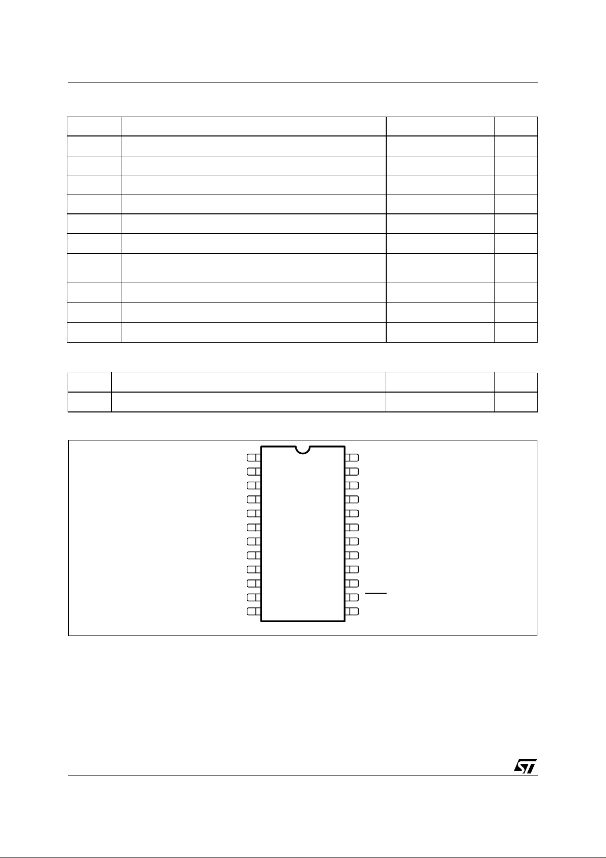
APPLICATION DIAGRAM
C
SS
July 2002
5V
25V
PGOOD
OVP
ILIM
SS
SHDN
VID4:0
VDR
VCC
L6996
OSC
BOOT
HGATE
PHASE
LGATE
PGND
GND
CS+
VFB-
VFB+
VPROG
HS
LS
CS-
C
VPROG
5V
L
R
V
SENSE
OUT
1.25
DS
1/26
L6996
ABSOLUTE MAXIMUM RATINGS
Symbol
Parameter
Value Unit
V
CC
V
DR
VCC to GND -0.3 to 6 V
V
to GND -0.3 to 6 V
DR
HGATE and BOOT, to PHASE -0.3 to 6 V
HGATE and BOOT, to PGND -0.3 to 36 V
V
PHASE
PHASE -0.3 to 30 V
LGATE to PGND -0.3 to VDR+0.3 V
ILIM, VFB+, VFB-, CS-, CS+, SHDN, VID0-4, PGOOD, OVP,
-0.3 to VCC+0.3 V
VPROG to GND
P
tot
T
T
stg
Maximum Power dissipation at T
Junction operating temperature range 0 to 125 °C
j
= 25°C 1 W
amb
Storage temperature range -55 to 125 °C
THERMA L D ATA
Symbol Parameter Value Unit
R
th j-amb
Thermal Resistance Junction to Ambient 125 °C/ W
PIN CONNECTION
VID2
VID1
VID0
CS-
CS+
VCC
GND
VPROG
VFB+
VFBOSC
SS
2
3
4
5
6
7
8
9
10
11
12
TSSOP24
24
23
22
21
20
19
18
17
16
15
14
13
VID31
VID4
BOOT
HGATE
PHASE
VDR
LGATE
PGND
PGOOD
OVP
SHDN
ILIM
2/26

PIN FUNCTIONS
N Name Description
L6996
1,2,3,
23,24
4 CS- This pin is used for both current sensing and to detect overvoltage and undervoltage
5 CS+ Current sense pin. Overcurrent condition is detected by sensing CS+ to CS- voltage.
6 VCC Supply voltage for analogy blocks. Connect it to 5V bus.
7 GND Signal ground
8 VPROG DAC output voltage. This pin provides the voltage programmed by the DAC. Connect a 10nF
9 VFB+ PWM comparator reference input. Connect this pin to VPROG.
10 VFB- PWM comparator feedback input, to be connected to the regulated output.
11 OSC Connect this pin to the battery through a voltage divider in order to provide the voltage
12 SS Soft start pin. 5µA constant current charges an external capacitor whose value sets the soft-
13 ILIM An external resistor connected between this pin and GND sets the current limit threshold.
VID4-0 V oltage Identification inputs. VID0 is the LSB and VID4 is the MSB for the DAC (see VID table)
conditions.
capacitor between this pin and GND.
An additional external voltage divider between output and VPROG may be used to realize the
active droop function.
By inserting a resistor between this pin and the regulated output, a positive offset can be
added to the output voltage.
feedforward feature.
start time.
14 SHDN
15 OVP Open drain output. The pull-down transistor is off either in OV condition or during a VID
16 PGOOD Open drain output. The pull-down transistor is on during soft-start, dynamic transitions and
17 PGND Po wer Ground. This pin has to be connected close to the low side MOSFET source in order to
18 LGATE Lower MOSFET gate driver output.
19 V
20 PHASE This pin provides the return path of the high side driver.
21 HGATE High side MOSFET driver output.
22 BOOT Bootstrap capacitor pin. The high side driver is supplied through this pin.
DR
ShutDown input. When connected to GND the device stops working. When high, it enables
the IC operation.
transition.
when an output voltage fault occurs.
minimize switching noise.
Voltage supply for the low side internal driver.
3/26

L6996
ELECTRICAL CHARACTERISTICS
(VCC = VDR = 5V; T
Symbol Parameter Test Condition Min. Typ. Max. Unit
SUPPLY SECTION
Vin Input voltage range Vout=1V Fsw=110Khz Iout=1A 1 28 V
Vcc, V
DR
Vccoff Turn-off voltage 4.1 4.3 V
V
HYST
Iqcc
(V
Iqcc
(Vcc)
SHUTDOWN SECTION
SHDN SHDN Threshold 0.6 1.2 V
I
(VDR)
I
SH
SOFT START SECTION
I
ON TIME
Ton On time duration Vprog=CS- =1.15 Osc=250mV 720 800 880 ns
OFF TIME
DAC
Vprog Voltage Accuracy VID0-4 see table 1 -1 +1 %
PWM COMPARATOR
I
VFB-
CURRENT LIMIT AND ZERO CURRENT COMPARATOR
I
PHASE-
GND
GATE DRIVERS
PROTECTIONS
OVP Over voltage trip CS- rising 117 120 123 %
UVLO Hysteresys 60 90 100 mV
Quiescent current driver VFB- > VFB+ 20 µA
)
DR
Quiescent current VFB- > VFB+ 600 µA
Driver quiescent current in
SH
shutdown.
(Vcc) Shut down current SHDN to GND 15 µA
SS charge current 4 6 µA
SS
Soft-start active range 0.9 V
Minimum Off Time 580 ns
K
OSC/TOFFMIN
Input voltage offset V
Input bias current (VP) V
ILIM input bias current CS-=V
LIM
K
Positive and negative Current
C
Limit factor.
Zero Crossing Comparator offset -2 2 mV
High side rise time V
High side fall time 50 70 ns
Low side rise time 50 70 ns
Low side fall time 50 70 ns
= 0°C to 70°C unless otherwise specified)
amb
SHDN to GND 5 µA
Vprog=CS-= 1.15 Osc= 500m V 355 420 485 ns
Vprog=CS-= 1.15 Osc= 1V 210 250 290 ns
Vprog=CS-= 1.15 Osc= 2V 120 150 180 ns
OSC=250mV
PROG
VFB-
V
=1.6V=V
=1.6V 4 5 6 µA
=1.6V
PROG
ILIM to GND = 120KΩ
R
= 120 KΩ 0.18 0.3 0.24 µA
ILIM
=5V; C=7nF
DR
HGATE - PHASE from 2 to 4.5V
PROG
FB-
=CS-=1.15V
4.5 5.5 V
0.28
-2 +2 mV
4.95 µA
50 70 ns
4/26
L6996
ELECTRICAL CHARACTERISTICS
(V
= VDR = 5V; T
CC
Symbol Parameter Test Condition Min. Typ. Max. Unit
UVP Under voltage trip CS- falling 66 69 72 %
PGOOD Upper threshold
PGOOD Lower threshold
Ron
P
GOOD
(CS-/V
(CS-/V
= 0°C to 70°C unless otherwise specified)
amb
)
PROG
)
PROG
(continued)
CS- rising; PGOOD active 109 112 115 %
CS- falling; PGOOD active 84 87 90 %
I
=2mA 40 60 100 Ω
SOURCE
Table 1. DAC Output Voltage
VID4 VID3 VID2 VID1 VID0 Output Voltage (V)
11 1 1 1 0.600
11 1 1 0 0.625
11 1 0 1 0.650
11 1 0 0 0.675
11 0 1 1 0.700
11 0 1 0 0.725
11 0 0 1 0.750
11 0 0 0 0.775
10 1 1 1 0.800
10 1 1 0 0.825
10 1 0 1 0.850
10 1 0 0 0.875
10 0 1 1 0.900
10 0 1 0 0.925
10 0 0 1 0.950
10 0 0 0 0.975
01 1 1 1 1.000
01 1 1 0 1.050
01 1 0 1 1.100
01 1 0 0 1.150
01 0 1 1 1.200
01 0 1 0 1.250
01 0 0 1 1.300
01 0 0 0 1.350
00 1 1 1 1.400
00 1 1 0 1.450
00 1 0 1 1.500
00 1 0 0 1.550
00 0 1 1 1.600
00 0 1 0 1.650
00 0 0 1 1.700
00 0 0 0 1.750
5/26

L6996
Figure 1. Funct i on a l & Blo c k D iag ram
IN
V
5V
OUT
V
GNDVCC
overvoltage comparator
BOOT
HGATE
HS driver
VCC
level shifter
V(LGATE)<0.5V
comp
LS and HS anti-cross-conduction comparators
R Q
0.6 VPROG
CS-
1.12 VPROG
CS+
-
+
-
undervoltage comparator
RS
pgood comparators
CS-
CS-
1.075 VPROG
0.925 VPROGpower management
+
-
+
-
PHASE
comp
V(PHASE)<0.2V
S
Toff min
delay
VDR
Ton min
one-shot
PGND
LGATE
LS driver
Q
R
S
Ton
one-shot
Ton
OSC
CS-
Q
S
one-shot
OSC
CS-
R
negative current limit
comparator
Ton= Kosc V(CS-)/V(OSC)
CS+
-
mode
dynamic
transition
+
mode
dynamic
transition
PHASE
80 us
one-shot
ILIM
0.05
CS-
-
+
+
zero-cross comparator
Ton= Kosc V(CS-)/V(OSC)
detection
transition
dynamic
6/26
OVPPGOODSHDN
VID4:0
dynamic transition control
IC enable
soft-start
control
+
+
-
comparator
positive current limit
5 uA
SS
ILIM
CS+
CS-
+
-
0.05
FB+
HS control
pwm comparator
5 uA
FB-
OSC
IN
V
1.236V
bandgap
5 bit DAC
1.416
VPROG
VID4:0
DAC
LS control
Reference chain
configuration

TYPICAL OPERATING CHARACTE RISTICS
The test conditions refer to the component list the table 5. VIN = 20V V
unless otherwise noted.
Figure 2. Dynamic Output Voltage Transition
Figure 5. Sta rt up with Zero Load
1.55V -> 1.35V
= 1.8V FSW = 270kHz T
OUT
amb
L6996
= 25°C
CH1 -> V
CH2 -> V
CH4 -> IL
PHASE
OUT
Figure 3. Dynamic Output Voltage Transition
1.35V -> 1.55V
CH1 -> V
CH2 -> V
CH4 -> IL
PHASE
OUT
Figure 6. Start up w ith 10A
CH1 -> V
CH2 -> SS
CH3 -> I
CH1 -> V
CH2 -> SS
CH3 -> I
L
OUT
L
OUT
Figure 4. Load Transient 0-15A
CH1 -> V
CH2 -> V
CH4 -> IL
OUT
OUT
7/26
L6996
Figure 7. Tes t Condition: Vin = 20V, V5v=5V, Fsw = 300kHz, T
[%]
Vout=1.7
Vout=1.25
Current [A ]
[%]
Vin=7
Vin=20
Current [A]
0.88
0.86
0.84
0.82
0.8
0.78
0.76
Figure 8. Tes t Condition: V
0.92
0.91
0.9
0.89
0.88
0.87
0.86
0.85
0.84
0.83
0.82
0.81
Efficency
Vout=1.35
0.10 1.00 10.00 100.00
= 1.75V, Fsw = 300kHz, V5v = 5V, T
out
Efficency
0.1 1.0 10.0 10 0.0
amb
Vin=12
= +25°C
= +25°C
amb
Figure 9. Tes t Condition: V
410
390
370
350
330
310
290
270
250
8/26
= 1.75V, V5v = 5V, T
out
Frequency
Vin=7
Vin=12
4 5 6 7 8 9 10 11 12 13 14 15
= +25°C
amb
[KHz]
Vin=20
Current [A]

Figure 10. Typical Application with Active Voltage Droop
L6996
5V
OSC
BOOT
HGATE
PHASE
LGATE
PGND
GND
CS+
CS-
VFB-
VFB+
VPROG
R
VIN2
C
VPROG
HS
LS
R
VP3
C
VIN1
C
C
BOOT
DS
C
VP3
R
R
C
V51
C
V52
R
PU2
R
PU1
M
IL
C
SS
V5
VCC
PGOOD
OVP
R
IL1
ILIM
R
IL2
SS
SHDN
VID4:0
VIN1
VDR
L6996
Figure 11. Typical Application without Active Voltage Droop
VIN2
D
BOOT
L
R
R
V
R
SENSE
VP2
IN
V
OUT
CPU
C
OUT
C
VP1VP1
C
OUT1
5V
R R
R
C
V51
C
V52
R
PU2
R
PU1
R
M
IL
C
SS
V5
VCC
PGOOD
OVP
IL1
R
ILIM
IL2
SS
SHDN
VID4:0
VIN1
VDR
L6996
OSC
BOOT
HGATE
PHASE
LGATE
PGND
GND
CS+
CS-
VFB-
VFB+
VPROG
VIN2
HS
LS
C
VPROG
VIN1
C
DS
C
C
BOOT
VIN2
D
BOOT
V
IN
L
R
SENSE
V
OUT
CPU
C
OUT
C
OUT1
9/26

L6996
1 DEVICE DESCRIPTION
1.1 Constant On Time PWM Topology
Figure 12. Loop block schematic diagram
Vin
R1
R2
VID0-4
OSC
CS-
Vprog
VFB+
VFB-
One-shot generator
R
S
DAC
+
+
-
-
PWM comparator
FFSR
Q
HGA TE
Q
LGA TE
HS
LS
DS
Rsense
Vout
This device implements a Constant On Time control, where the Ton is the on time duration forced by a one-shot
circuit. The controller calculates the one-shot time directly proportional to the V
pin voltage and inversely to
CS-
the OSC pin voltage as in Eq 1:
V
CS-
Eq 1
where K
=180ns and τ is the internal propagation delay time (Typ. 40ns). The system imposes in steady
OSC
T
ON
K
OSC
-------------- -
V
OSC
state a minimum on time corresponding to V
responding Ton will not decrease. Connecting OSC pin to a voltage partition from V
state switching frequency F
Eq 2
independent of VIN. It results:
SW
V
OUT
F
SW
-------------- -
---------- -
⋅α
T
V
IN
τ+=
= 2V. In fact if the V
OSC
1
→
ON
OSC
OSC
⋅==
F
SWKOSC
voltage increases above 2V the cor-
to GND, it allows steady-
IN
where
V
OSC
Eq 3
α
OSC
-------------- -
V
IN
R
2
--------------------==
+
R2R
1
The above equations allow setting the frequency divider ratio aOSC once output voltage has been set; note that
such equations hold only if V
<2.A minimum off-time constrain of about 500nS is introduced in order to as-
OSC
sure the boot capacitor charge and to limit switching frequency after a load transient as well as to mask PWM
comparator output against switching noise and spikes.
The system has not an internal clock, b ecause this is a hysteretic control ler, so the turn on pulse will star t if three
10/26

L6996
conditions are met contemporarily: the PWM comparator output is low (i.e. the output voltage is below the reference voltage), the minim um off time is pas sed and the current limit comparator is not triggered ( i.e. the i nductor current is unde r the current li mit programmed value) . The voltage on the O SC pin must range between 50mV
and 2V to ensure the system linearity.
1.2 Closing the loop
The loop is cl osed connecting the output voltage to the FB- pin. The FB- pin is linked internally to the comparator
negative pin and the positive pin is connected to the programmed voltage as in Figure 12. When the FB- goes
lower than FB+, the PWM comparator output goes high and sets the flip-flop output, turning on the high side
MOSFET. This condition is latched to avoid noise spike. After the on-time (calculated as described in the previous section) t he sys tem resets the fl ip- flop and then turns off the high side MOSFET and turns on the l ow side
MOSFET. Internally the device has more complex logic than a flip-flop to manage the transition in correct way.
For more details refers to the schematic Fig. 1. Because the sy stem implem ents a valley loop control, the average output voltage is different from the programmed one as shown in figure 13.
Figure 13. Valley Regulation
V out
DC Error Offset
Figure 14. Voltage positioning network
To inductor
PWM
COMPARATOR
+
L6996
VFB-
VFB+
Vprog
Rsense
R4
R2
<Vout>
Vref
Time
T o Vout
R1
R3
The L6996 performs an externally adjustable active droop, achieving a 4m V/A load line slope using a 1.5m
Ω
sense resistor without use an external amplifier. F ocusing the attention on the control part of the system (Figure
14), it can be considered that the inductor current can r evert (t he PFM function is deal towards) and the curr ent
11/26

L6996
has an average value equal to Io. The intention is to find the output average value called Vo. It is important to
remember that the loop is clos ed a v alley of the ripple, in this conditi ons the inputs of PWM comparator must be
equal, so the VFB+ =VFB-. Suppose R4=0 and R3=open.
Considering this and watching the figure 14 it can be written two equations at the VFB+ and VFB- node:
Eq 4 Rsense · Io = Vc
Eq 5
V
ovalleyVprog
----------------------------------- ------------------------ -Vc=
–()
+
R1 R2
Imposing Eq4=Eq5 it can be found the V
⋅
R1
OVALLEY
value:
Eq 6 Vovalley = Vprog + Rs · (1 + R1/R2) · Io
Form Eq6 it can be noted the active drop effect due to R 1, R2 resi stors; it c an be also noted the o utput aver age
value is different from the V
value, the error is due to the valley control, and it is equal to half of the ESR
PROG
voltage ripple.
To reduce the error of the average output voltage w e can change the V
value using resistors. In fact con-
PROG
sidering the R3 resistor we can make a Thevenin equivalent:
Eq 7 Vprogeq = Vprog · R3/(R3 + R2)
Eq 8 Req = R3//R2
How it can be seen the V
that the R1, R2 and R
SENSE
PROGEQ
is less the V
and so we can reduce the av er age output error . R emember
PROG
are selected in base at the Voltage Positioning needs.
The R4 resistor can be used to set also a positive offset at zero load. C onsidering the PWM compar ator inputs:
Eq 9 Vo = V
+ R4 · 5µA
FB+
Respect to a traditional PWM controller, that has an internal osci llator setting the switchi ng frequency, in a hysteretic system the frequency can change with some parameters (input voltage, output current). In L6996 is implemented the voltage feed-forward circuit that allows constant switching frequency during steady-sate
operation with the input voltage variation. There are many factors affecting switching frequency accuracy in
steady-state operation. Some of these are internal as dead times, which depend on high side MOSFET driver.
Others related to the external components as high side MOSFET gate charge and gate resistance, voltage
drops on supply and ground rails, low side and high side RDS
and inductor parasitic resistance.
ON
During a posi tive load trans ient, (the output current incr eases), the converter switches at its maxi mum frequency
(the period is TON+TOFFmin) to recover the output voltage drop. During a negative load transient, (the output
current decreases), the device stops to switch (high side MOSFET remains off).
1.3 Transition from PWM to PFM
To achieve high efficiency at light load condition s, PFM mode is provided. The PFM mode differs from the PWM
mode essentially for the off section; the on section is the same. In PFM after a turn-on cycle the system turnson the low side MOSFET, until the current reaches the zero A value, when the zero-crossing comparator turns
off the low side MOSF ET. In this way the energy stored in the output capacitor will not flow to ground, through
the low side MOSFET, but it will f l ow to the load. In P WM mode, aft er a tur n on cycl e, the system keeps the low
side MOSFET on until the next turn-on cycle, so the energy stored in the output capacitor will flow through the
low side MOSFET to ground. The PFM mode is naturally implemented in hysteretic controller, in fact in PFM
mode the system reads the output voltage with a comparator and then turns on the high side MOSFET when
the output voltage goes down a reference value. The device works in discontinuous mode at light load and in
12/26

L6996
continuous mode at high load. The transition from PFM to PWM occurs when load current is around half the
inductor current rippl e. This threshold value depends on V
ue is, the smaller the threshold is. On the other hand, the bigger the inductor value is, the slower the transient
response is. In PFM mode the frequency changes, with the output current changing, more than in PWM mode;
in fact if the output current increase, the output voltage decreases more quickly; so the successive turn-on arrives before, increasing the switching frequency. The PFM waveforms may appear more noisy and asynchronous than normal operation, but this is normal behaviour mainly due to the very low load. The NOSKIP feature
cannot be disabled.
1.4 Softstart
If the supply v oltages are alr eady applied , the SH DN pin gives the start- up. The sys tem s tarts w ith the high s ide
MOSFET off and the low side MOSFET on. After the SHDN pin is turned on the SS pin voltage begins to increase and the system starts to switch. The softstart is realized by graduall y increasing the current limit thr eshold to avoid output overvoltage. The active soft start range (where the output current limit increase linearly)
starts from 0.6V to 1.5V. In this range an internal current source (5
The reference current (for the curr ent li mit com parator) forced through ILIM pin i s pr oportional to SS pin v oltage
and it saturates at 5
µ
A (typ.) when SS voltage is close to 1.5V; so the maximum current limit is active. Output
protections like undervoltage is disabled until SS pin voltage reaches 1.5V, instead the overvoltage is always
present.
Once the SS pin voltage reaches the 1.5V value, the voltage on SS pin doesn't impact the system operation
anymore. If the SHDN pin is turned on before the supplies, the correct start-up sequence is the follow ing: first
turn-on the power section and after the logic section (V
CC
IN
pin).
, L, and V
µ
. Note that the higher the inductor val-
OUT
A typ) charges the capacitor on the SS pin.
Figure 15. Soft-start diagram
Vss
4.1V
1.5V
0.6V
Ilim current
5
A
µ
Soft-start active range
Time
Maximum current limit
Time
1.5 Current limit
The current limit comparator senses inductor current through the sense resistor when the low side MOSFET is
on and compares this value with the ILIM pin voltage. While the current is above the prefixed value, the control
inhibits the one-shot start.
To properly set the current limit threshold, it should be noted that this is a valley current limit. A verage current
depends on the inductor value, V
IN
e V
OUT
.
Eq 10 I
OUT
= I
CL
MAX_VALLEY
+ ∆IL / 2
13/26

L6996
To set the current threshold, choose R
Eq 11
Where K
is the current limit factor (0.25µA typ.). A negative current l imit is als o introduced during dynamic tran-
C
I
MAX_VALLEY
according to the following equation:
ILIM
R
ILIM
--------------------- -
R
SENSE
⋅=
K
C
sitions, when zero-cross comparator is disabled and at the inductor current is allowed to reverse. The negative
current limit is useful w hen performing a negativ e transition ( that is , output voltage i s reduced) to avoid too high
discharging current.
Both positive and negative c urrent limit have the same threshold; but the negative c urrent l imit c an be set using
the OVP signal plus a transistor, that changes during the dynamic transition, as in Fig. 16 (Q5, R11).
The system accuracy is func tion of the exactness of the r esi stance c onnected to I
pin and RSENSE resistor.
LIM
Moreover the voltage on ILIM pin must range between 10mV and 2V to ensure the system linearity.
1.6 Protection and fault
Sensing CS- pin voltage performs the output protection. The nature of the fault (that is, latched OV or latched
UV) is given by the PGOOD and OVP pins. If the output voltage is within the 90% 110% range, PGOOD is high.
If an overvoltage or an undervoltage occurs, the dev ice is latched. l ow side MOSFET is turned ON and high s ide
MOSFET off. PGOOD goes low. OVP goes high in case of overvoltage, allowing the fault nature to be detected.
To recuperate the functionality either the device must be shut down, thought the SHDN pin, or the supply has
to be removed. These features ar e useful to protec t against short- circuit (UV fault) as well as hi gh side MOSFET
short (OV fault).
1.7 Drivers
The integrated high-current dri vers all ow using different size of power MOSFET, maintaini ng fast switching transition. The driver for the high side MOSFET uses the BOOT pin for supply and PHASE pin for return (floating
driver). The driver for the low side MOSFET uses the VDR pin for the supply and PGND pin for the return. The
main feature is the adaptive anti-cross-conduction protection, which prevents from both high side and low side
MOSFET to be on at the sam e time, avoiding a high current to flow from VIN to GND. When high side MOSFET
is turned off the voltage on the pin PHASE begins to fall; the low side MOSFET is turned on only when the voltage on PHASE pin reaches 250mV. When low side is turned off, high side remains off until LGATE pin voltage
reaches 500mV. This is impor tant since the driver can wor k properly wi th a l arge range of external power MOSFETS.
The current necessary to switch the external MOSFETS flows through the device, and it is proportional to the
root square of the MOSFET gate charge and the switching frequency. So the power dissipation of the device is
function of the external power MOSFET gate charge and switching frequency.
Eq 12 P
driver
= VCC · Q
gTOT
· F
SW
The maximum gate charge values for the low side and high side are given from:
f
SW0
------------ -
⋅=
Eq 13
Eq 14
Where f
= 500kHz. The equations above ar e valid for TJ = 150°C. If the system temperature is lower the Q
SW0
Q
MAXHS
Q
MAXLS
f
------------ -
f
SW
SW0
f
SW
75nC
⋅=
125nC
can be higher.
For the Low Side driver the max output gate charge meets another limit due to the internal traces degradation;
14/26
G

L6996
in this case the maximum value is Q
MAXLS
= 125nC.
The low side driver has been designed to have a low resistance pull-down transistor, around 0.5 ohms. This
prevents the voltage on LGATE pin raises during the fast rise-time of the pin PHASE, due to the Miller effect.
1.8 Digi tal to analog converter
The built-in digital to analog converter ( DAC) allows the adjustment of the output voltage in correspondence to
the Table1 in pag 4: from 0.6V to 1V with 25mV steps, and from 1V to 1.75V with 50mV steps. The DAC can
receive the digital input from the CPU. The programmed voltage is available on VPROG pin, which is capable
of sourcing or sinking up to 250
µ
A. The internal reference accuracy is ±1%.
1.9 Dynamically changing DAC code
L6996 detects as a transition any change in VID code which duration is larger than 200ns. Then, a timer forces
the chip in a 'transition state' for about 100µs. In such a state, output protections ar e disabled and OVP pin goes
high.
Current limit threshol d can be r educed during the t ransition state dur ation by us ing an external m os shorting par t
of the R
resistor. The MOSFET gate is driven by OVP. Reducing current limi t threshold prevents from output
ILIM
voltage overshoot/undershoot once the new-programmed voltage has been reached (see waveforms reported
below), especially when the droop is not implemented. Note that the reduced threshold must be however high
enough to allow the output capacitor to charge/discharge within the transition time. During the transition state
duration, zero-cross comparator is disabled and inductor current is allowed to reverse. A negative current limit
is introduced. During OFF time, if inductor current is negative and reaches the threshold, low side MOSFET is
forced OFF, and remain OFF, allowing negative current to flow across high side body diode, for at least T
ON
After then, the low side or high side turns ON again, depending on PWM comparator output. This allows switching frequency to be close to steady state fr equency al so when t he device wor ks in neg ative curr ent li mit protection.
Dynamically changing the VID code is useful for portable computers, where the CPU is supply at a higher voltage when the AC-DC adapter is plugged-in, to increase speed. A lower voltage is instead provided when only
the battery powers the CPU, to save energy.
The dynamic transition is usually made at light load condition, to allow the full current to be available for charging/discharging the output capacitor:
Iout ~ 300mA
∆
Vout
~250mV
max
The current limit threshold should be set high enough to charge/discharge the output capacitor within the transition state duration (see below). If the output voltage changing is higher than 250mV the system can detect an
overvoltage or undervoltage that can shut down the device.
.
15/26

L6996
t
2 APPLICATION INFORMATION
2.1 Demo bo ar d descr iption
The demoboard shows the device operation in general purpose applications. The evaluation board needs two
different supplies; one for the IC section (5V), and anoth er for the conversi on section (up to 28V). Output current
in excess of 20A can be r eached depe ndently o n the MO SFET type. The SW1 is us ed to s t art the dev ice (w hen
the supplies are already present) and to select the VID code (i.e. the output voltage).
Figure 16. Schematic Diagram
PGOOD
OVP
R2..R6 R1
VID4:0
Q5
+5V+5V
+5V+5V
R11
SHDN
R24
DPSLP
C4
R9R7
R10
C11
C10
+5V
R8
PGOOD
OVP
ILIM
SS
SHDN
VID4:0
R19
GMUXSEL
VCC
VDR
L6996
U1
+5V
C9
R16
OSC
BOOT
HGATE
PHASE
LGATE
PGND
GND
CS+
VFB-
VFB+
VPROG
+5V
U9
+5V
U7
CS-
R15
+5V
C6
+5V
U2
+5V
U8
+5V
U6
Q1,2
Q3,4,5
R12
R18
+5V
C1
GND
VIN
D1
C7
C5
L1
D2
VPR
+5V
U3
+5V
U4
+5V
U5
DPSL VR
C12..C17
R14
R17
R13
R21R22R23
GND
Q8Q7Q6
VOUTSENSE
VOUT
C18..C23
GND
C8
R20
+5V
+5V
C2
C3
Rou
GNDSENSE
16/26

2.2 Demoboard Layout
L6996
Figure 17. PCB Board Layout - Layer one
(Top component side)
Figure 18. PCB Board Layout - Layer two
(Internal Gro und plane)
Figure 20. PCB Board Layout - Layer four
(Bottom component side)
Figure 21. PCB Board Layout
(Component position top view)
Figure 19. PCB Board Layout - Layer three
(Internal signal plane)
Figure 22. PCB Board Layout
(Compon e nt position bott om vi e w)
17/26

L6996
Table 2. PCB Layout guidelines
Goal Suggestion
Low radiation and low magnetic coupling with the
adjacent circuitry
Don’t penalty the efficiency Keep the power traces and load connections short and wide.
Ensure high accuracy in the current sense system Cs+, CS- traces must be made by Kelvin connection. Also the
Reduce the noise effects on IC 1) Put the feedback component (like the VP network as close
1) Small switching current loop areas. (For example Placing
C
, high side and Low Side MOSFET, Schottky diode, as
IN
close as possible each to others).
2) Controller placed as close as possible to the Power
MOSFET.
3) Group the gate drive component (Boot cap and diode
together near the IC.
traces should be separated from the power plane by a ground
plane, run parallel.
as possible to the IC)
2) The feedback connection (like the FB trace, or CS+/CStraces….) should be route as far as possible from the
switching current loops.
3) Make the controller ground connection like in the figure 16.
3 DESI GN EXAMPLES
3.1 V
= 20V I
IN
OUT
= 23A
In this design it is considered a low profile demoboard, so a great attention is given to the components height.
3.2 Inp ut capac itor
A pulsed current (with zero average value) flows through the input capacitor of a buck converter. The AC component of this current is quite high and dissipates a cons iderable amount of power on the ESR of the capacitor:
2
Vin Vin Vout
Eq 15
The I
current is given by:
RMS
Eq 16
P
CIN
Icin
ESR
rms
CIN
Iout
2
⋅⋅=
Iout
δ1δ–()
----------------------------------------------- -
δ
------
+=
12
–()⋅
2
Vin
2
∆()
I
L
Neglecting the last term, the equation reduces to:
Eq 17
, and also I
P
CIN
CINRMS
Icin
rms
, has a maximum equal to I
Ioutδ1
δ–()=
/2 (@ VIN = 2 × V
OUT
, that is, 50% duty cycle). The input,
OUT
therefore, should be selected for a RMS ripple current rating as high as half the respective maximum output
current. Electrolytic capacitor s are the most us ed because ar e the cheapest ones and ar e availabl e with a wide
range of RMS current ratings. The onl y drawback is that, c onsider ing a requested r ipple c urrent rati ng, they are
physically larger than other capaci tors. Very good tantal um capacitors are coming availa ble, with v ery low ESR
and small size. The only problem is that they occasionally can burn out if subjected to very high current during
the charge. So, it is better avoid this type of capacitors for the input filter of the device. In fact, they can be subjected to high surge current when connected to the power supply. If available for the requested value and voltage rating, the ceramic capacitors have usually a higher RMS current rating for a given physical size (due to the
very low ESR). From the equation 17 it is found:
18/26

L6996
Icin
= 6.4A
rms
Considering 10uF capacitors ceramic, that have ICINRMS =1.5A, 6 pzs. are needed.
3.3 Inductor selection
In order to determine the inductor value is necessary considering the maximum output current to decide the inductor current saturation. Once the inductor current saturation is found automatically it is found the inductor value also. The inductor value is important al so to determine the duration of the dynamic output voltage transi t ion.
In our design it is considered a very low profile inductor.
µ
L = 0.6
The saturation current for this choke is 25A
3.4 Output capacitors
The output capacitor is c hosen by the output v oltage static and dynamic accur acy. The static accuracy is related
to the output voltage ripple value, while the dynamic accuracy is related to the output current load step.
If the static precision is around +/- 4% for the 1.25V output voltage, the output accuracy is ±50mV.
To determine the ESR value from the output precision is necessary before calc ulate the ripple current:
Eq 18
∆
I
Vin Vo
---------------------- -
L
⋅⋅=
Vo
---------
Vin
T
sw
–
Considering a switching frequency around 270kHz from the equation above the ripple current is around 7A.
So the maximum ESR should be:
A
∆
V
Eq 19
ESR
ripple
-------------------- -
∆
I
---- -
2
50mV
----------------
3.5
14m
Ω===
The dynamic specifications are sometime more relaxed than the static requirements so the ESR value around
Ω
7m
should be enough.
Sometimes can be considered the output capacitor effect also:
2
⋅
L
Iout
Eq 20
∆
Vout
--------------------- -
⋅
2Vout
From the above equation can be calculated the minimum output capacitance value. Considering
100mV, C
Five capacitor of 330
> 1600µF should be used.
OUT
µ
F from PANASONIC correspond to the request. To allow the device control loop to prop-
1
------------- -⋅=
Cout
∆
V
=
OUT
erly work, output capacitor ESR zero must be at least ten times small er than switching frequency. Low ESR tantalum capacitors, which ESR zero is close to 10 kHz, are suitable for output filtering. Output capacitor value
COUT and its series resistance, should be large enough and small enough, respectively, to keep output voltage
within the accuracy range during a load transient, and to give the device a minimum signal to noise ratio.
The current ripple fl ows through the output capacitor, so the output capacitors should be calculated also to sustain this ripple: the RMS current value is given from Eq21.
1
---------- -
Eq 21
Icout
rms
23
∆=
I
L
But this is usually a negligible constrain when choosing output capacitor.
19/26

L6996
3.5 Pow er MO SFET an d Schottky Diod es
Since a 5V bus powers the gate drivers of the device, the use of logic-level MOSFET is highly recommended,
especially for high current applications. T he breakdown voltage V
certain margin, so the selection w ill address 20V or 30V devices (depends on applications).
The RDS
can be selected once the allowable power dissipation has been established. By selecting identical
ON
Power MOSFET as the main switch and the synchronous rectifier, the total power they dissipate does not depend on the duty cycle. Thus, if PON is this power loss (few percent of the rated output power), the required
RDS
Eq 22
α
(@ 25 °C) can be derived from:
ON
P
RDS
ON
------------------------------------------------ -=
Iout21
ON
αT∆⋅+()⋅
is the temperature coefficient of RDS(ON) (typically, a = 5*10-3 °C-1 for these low-voltage classes) and T the
admitted temperature rise. It is worth noticing, however, that generally the lower RDS
charge Q
, which leads to a higher gate drive consumption. In fact, each switching cycle, a charge QG moves
G
from the input source to ground, resulting in an equivalent drive current:
must be greater than VINMAX with a
BRDSS
, the higher is the gate
ON
Eq 23
Iq Q g F
⋅=
SW
The Schottky diode to be placed in parallel to the synchronous rectifier must have a reverse voltage VRRM
greater than VINMAX.
For this application are selected: two high side MOSFET STS11NF3LL and two STS17NF3LL for the low side
section.
3.6 RSE N SE selecti on
The droop function consists to change the output voltage changing the output current; at high output current the
output voltage is lower than the reference voltage. To implement the droop function, for the high current status,
we use the R
resistor in series to the inductor. Since inductor current can be very high, so the resistor
SENSE
must be capable to diss ipate high power. Moreover w e use the sense resi stor to measure the output cur rent for
the current limit feature, so the R
higher temperature stability it could possible to split the R
R
value must be as low as possible, so the Active voltage droop im plemented in L6996 is very useful. For
SENSE
value must be very accurate also for temperature variation. To ensure
SENSE
value. To achieve high efficiency also the
SENSE
this application it are selected two 3mohms resistors from PANASONIC.
3.7 VP Network Design
The voltage-positioning network is selected by the load regulation needed. In this application wit is considered
4mV/A; with a RSENSE r esis tor ar ound 1.5mo hms i t can be us ed a gain around 2.66 and so a rate between R1
and R2 around 1.66 from the Eq6.
It can be selected:
R1=1.66K
R2=1K
A capacitor C
Ω
Ω
is required in parallel with RVP1 to correctly compensate the network response. Its value is
VP1
given by the following equation:
Eq 24
where C
is the output capacitor value. When C
OUT
C
VP1
ESRC
⋅=
OUTCOUT
is well chosen, a step decrease of output voltage should
VP1
1
------------- -
R
VP1
--------------+
R
1
VP2
be observed, as an effect of a step load increase. Too small or too large C
instead of a step waveform.
20/26
produces overshoot or undershoot
VP1

With our parameter:
C
= 7.8pF
VP1
No-load offset is obtained by R
Eq 25
R
VP3
and of a current source internally connected to VFB+ pin. Thus:
VP3
V
OUT I,0
---------------------------------------------------- -
–
=
I
OFFSET
V
PROG
1
----------------------- -=
R
VP2
------------- -1+
R
VP1
L6996
where I
The capacitor C
Eq 26
OFFSET
= 5µA.
in parallel to R
VP3
C
VP3
is a filter which time constant can be the same as in Eq22, so
VP3
ESRC
------------------------------------------------ -=
⋅
OUTCOUT
R
VP3
3.8 Input divider
The input divider can be selected with the Eq1, Eq2, Eq3 . Choosing a switching frequency around 270kHz it
results:
R1 = 560K
R2 = 27K
α
OSC = 0.048.
Ω
Ω
3.9 Current limit resistor
From the Eq12 it can be set the current limit resistor, for the positive current limit; it results:
R10 + R11 = 120K
The negative current limit is set by the time available for the negative dynamic transition; a value around 30K
Ω
Ω
for R10 is a match between negative peak current and time to end the dynamic transition (around 80mS).
R10=150KW
R11=30KW
3.10Softstart capacitor
The soft start capacitor is selected once the soft start time is imposed. It can be consi der a soft start time around
1ms. The soft start capacitor is given by:
Eq 27
∆
Where
VSS is the soft start active range and ∆T is the soft stat time. From Eq 28 results: CSS = 10nF.
∆⋅
I
T
lim
SS
--------------------=
∆
V
ss
21/26
C

L6996
Table 3. Component List
The component list is shared in two sections: the first for logic and general-purpose component, the second for
power section:
GENERAL PURPOSE COMPONENTS
Part name Value Part number Manufacturer Notes
R1, R2, R3, R4, R5, R6,
R7, R9, R18, R19, R24
R8 47kΩ
R10 120kΩ Current limit resistors
R11 30kΩ
R12 1.66kΩ Voltage positioning
R13 1kΩ
R15 560kΩ Input resistor divider (to
R16 27kΩ
R20 130kΩ IMVPII resistor network
R21 39kΩ
R22 36kΩ
R23 270kΩ
33kΩ
(to set the current limit)
resistors
set the switching
frequency)
C1 47µF Tantalum/SP
C2, C3 100nF
C4 220nF
C5 220nF
C6 10nF
C7 220nF
C8 6.8nF Voltage positioning
C9 47pF
C10 10nF
C11 47pF
U2, U6, U8 Or gate NC7SZ32M5 FAIRCHILD Logic network
U9, U7 Inverter gate NC7SZ04P5 FAIRCHILD
U3,U4,U5 Nor gate NC7SZ02P5 FAIRCHILD
D1 BAT54A BAT54A PHILIPS
Q5,Q6,Q7,Q8 BSS131 Q62702-S565 INFINEON
SW1, SW2 DIP SWITCH *1
capacitor
22/26

L6996
POWER SECTION
SENSE RESISTOR
Part name Value Part number Manufacturer Notes
R14, R17 3mΩ ER JM1W SF3 M0U PANASONIC 1%
It is important, for this component, to keep in mind three factor: it must be able to dissipate high power. Again
its variation with the temperature must be small and the precision must be high to ensure high precision with the
ST voltage droop function.
INPUT CAPACITOR
Part name Value Part number Manufacturer Notes
C12,C13,C14,C15,C16,C17 10µF ECJ5YB1E106M PANASONIC 25V ceramic
10µF ECJ5YF1E106M PANASONIC 25V ceramic
10µF C34Y5U1E106ZTE12 TOKIN 25V ceramic
10µF GMK325F106ZH TAIYO-YUDEN 35V ceramic
10µF TMK325F106ZH TAIYO-YUDEN 25V ceramic
10µF TMK432BJ106MM TAIYO-YUDEN 25V ceramic
For this components can be useful control the temperature coefficient and the equivalent serie resistor and the
voltage rated.
OUTPUT CAPACITOR
Part name Value Part number Manufacturer Notes
C18,C19,C20,C21,C22,C23 270µF EEFUE0D271R PANASONIC 2V
C18,C19,C20,C21,C22 330µF EEFUE0D271R PANASONIC 2V
For this components can be useful control the temperature coefficient and the equivalent series resis tor and the
voltage rated.
INDUCTOR
Part name Value Part number Manufacturer Notes
L1 0.6µF ETQP6F0R6BFA PANASONIC
0.6µF A959AS-R60N TOKO
0.6µF CEP12D38H-0R6 SUMIDA
For the inductor important fac tors ar e the saturati on curr ent and the equi valent s eries r esist or (for the efficienc y
improvements)
POWER MOS
Part name Value Part number Manufacturer Notes
High side
Q1, Q2 STS11NF3LL STS11F3LL STMicroelectronics
STSJ25NF3LL STSJ25NF3LL STMicroelectronics
Low Side
Q3, Q4 STS17NH3LL STS17NH3LL STMicroelectronics Q5 N.M
STS25NH3LL STS25NH3LL STMicroelectronics .
Note N.M.=Not Mounted.
For the MOSFET choose is important to know the input voltage and output voltage. The MOSFET must able
23/26

L6996
dissipate high power (for switching losses or conduction losses).
POWER DIODES
Part name Value Part number Manufacturer Notes
D2 STPS2L25U STPS2L25U STMICROELECTRONICS 25V
This component must have low forward voltage and must have high reverse voltage (at least equal at the input
voltage).
24/26

mm inch
DIM.
MIN. TYP. MAX. MIN. TYP. MAX.
A 1.20 0.047
A1 0.05 0.15 0.002 0.006
A2 0.80 1.00 1.05 0.031 0.039 0.041
b 0.19 0.30 0.007 0.012
c 0.09 0.20 0.003 0.008
D 7.70 7.80 7.90 0.303 0.307 0.311
E 6.40 0.252
E1 4.30 4.40 4.50 0.170 0.173 0.177
e 0.65 0.025
L 0.45 0.60 0.75 0.018 0.024 0.030
L6996
OUTLINE AND
MECHANICAL DA T A
L1 1.00 0.039
k 0˚ min., 8˚ max.
TSSOP24
Thin Shrink Small Outline Package
7100777 (JEDEC MO-153-AD)
25/26

L6996
Information furnished is believed to be accurate and reliable. However, STMicroelectronics assumes no responsibility for the consequences
of use of such information nor for any infringement of patents or other rights of third parties which may result from its use. No license is granted
by implic ation or oth erwise unde r any paten t or patent ri ghts of STMi croelectroni cs. Speci fications me ntioned in this publication are s ubj ect
to change without notice. This publication supersedes and replaces all information previously supplied. STMicroelectronics product s are not
authorized for use as critical components in life su pport device s or systems without express written approval of STMicroelectronics.
The ST logo is a registered trademark of STMicroelectronics
© 2002 STMic roelectronics - All Right s Reserved
Australia - Brazil - Canada - Chi na - F i nl and - France - Germany - Hong Kong - India - Israel - Ital y - J apan -Malay si a - Malta - Morocco -
Singap ore - Spain - Sw eden - Switzerl and - United K i ngdom - United States.
STMicroelectronics GROUP OF COMPANIES
http://www.s t. com
26/26
 Loading...