

STEP DOWN CONTROLLER FOR HIGH DIFFERENTIAL
FEATURE
■ CONSTANT ON TIME TOPOLOG Y ALLO WS
OPERATION WITH LOWER DUTY THAN
PWM TOPOLOGY
■ VERY FAST LOAD TRANSIENTS
■ 5V V
■ 1.5V TO 28V INPUT VOLTAGE RANGE
■ 0.9V ±1% V
■
■ SELECTABLE SINKING MODE
■ LOSSLESS CURRENT LIMIT
■ REMOTE SENSING
■ OVP,UVP LATCHED PROTECTIONS
■ 600µA TYP QUIESCENT CURRENT
■ POWER GOOD AND OVP SIGNALS
■ PULSE SKIPPING AT LIGHT LOADS
APPLICATIONS
■ I/O BUS FOR CPU CORE SUPPLY
■ NOTEBOOK COMPUTERS
■ NETWORKING DC-DC
■ DISTRIBUTED POWER
SUPPLY
cc
REF
MINIMUM OUTPUT VOLTAGE AS LOW AS 0.9V
L6995
INPUT-OUTPUT CONVERSION
TSSOP20
ORDERING NUMBERS: L6995D
L6995DTR
DESCRIPTION
The device is a step-down controller specifically designed to provide extremely high efficiency conversion, with losses current sensing tecnique.
The "constant on-time" topology assures fast load
transient response. The embedded "voltage feed- forward" provides nearly constant switching frequency
operation.
An integrator can be introduced in the control loop to
reduce the static output voltage error.
The available remote sensing improve the static and
dynamic regulation recovering the wires voltage
drop. Pulse skipping technique reduces power consumption at light load. Drivers current capability allows output current in excess of 20A.
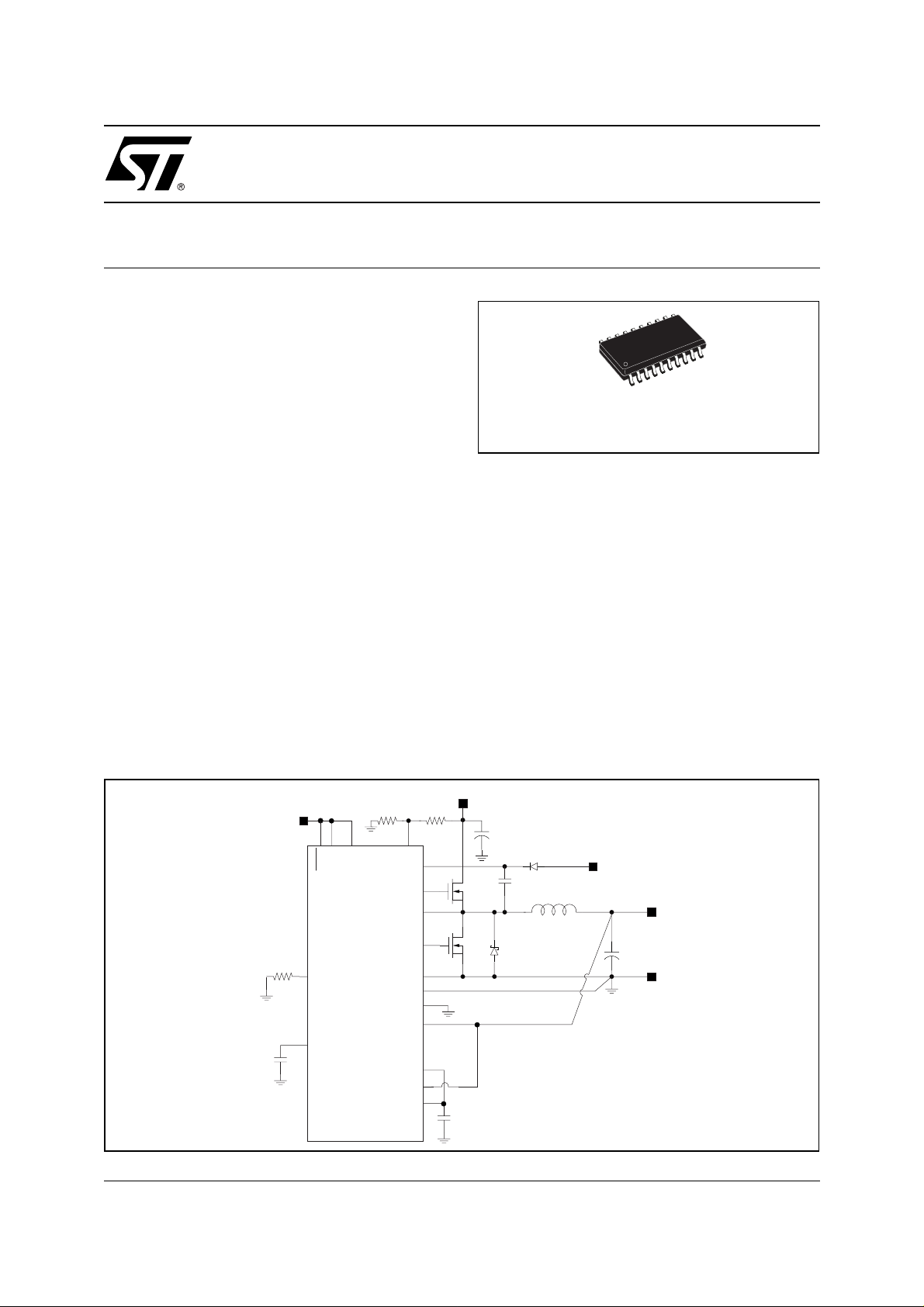
MINIMUM COMPONENT COUNT APPLICATION
Rin2 Rin1
5V
OSC
VDR
VCC
SHDN
RILIM
ILIM
L6995
SS
C
SS
BOOT
HGATE
PHASE
LGATE
PGND
GND
NOSKIP
VSENSE
INT
VFB
VREF
December 2002
This is preliminary information on a new product now in development. Details are subject to change without notice.
28V
C
HS
LS
VREF
CIN
D
BOOT
C
BOOT
L
DS
5V
C
OUT
Vo
0.9V
1/25
L6995
ABSOLUTE MAXIMUM RATINGS
Symbol Parameter Value Unit
V
CC
V
DR
V
PHASE
P
tot
T
stg
THERMAL DATA
Symbol Parameter Value Unit
VCC to GND -0.3 to 6 V
V
to GND -0.3 to 6 V
DR
HGATE and BOOT, to PHASE -0.3 to 6 V
HGATE and BOOT, to PGND -0.3 to 36 V
PHASE -0.3-to 30 V
LGATE to PGND -0.3 to V
ILIM, VFB, VSENSE, NOSKIP, SHDN, PGOOD, OVP, VREF, INT,
SENSE
to GND
= 25°C 1 W
amb
GND
Power dissipation at T
-0.3 to V
+0.3 V
DR
+0.3 V
CC
Storage temperature range -40 to 150 °C
R
th j-amb
PIN CONNECTION
Thermal Resistance Junction to Ambient 125 °C/W
T
Junction operating temperature range 0 to 125 °C
j
(Top View)
NOSKIP
GNDSENSE
INT
INT
VSENSE
VCC
GND
VREF
VFB
OSC
2
3
4
5
6
7
8
9
10SS
TSSOP20
20
BOOT1
19
HGATE
18
PHASE
17
VDR
16
LGATE
15
PGND
14
PGOOD
13
OVP
12
SHDN
11
ILIM
PIN FUNCTION
N° Name Description
1 NOSKIP Connect to V
2 GNDSE
Remote ground sensing pin
NSE
3 INT Integrator output. Short this pin to VFB pin and connect it via a capacitor to V
integrator in the control loop. If the integrator is not used, short this pin to VREF.
4 VSENSEThis pin must be connected to the remote output voltage to detect overvoltage and undervoltage
conditions and to provide integrator feedback input.
5V
Supply voltage for IC core. Connect to 5V bus.
CC
6 GND Signal ground
7 VREF 0.9 V voltage reference. Connect max. a 10nF ceramic capacitor between this pin and ground.
This pin is capable to source or sink up to 250uA
to force continuous conduction mode and sink mode.
CC
to insert the
OUT
2/25
L6995
PIN FUNCTION
(continued)
N° Name Description
8 VFB PWM comparator feedback input. Short this pin to INT pin when using the integrator function, or
to VSENSE pin without integrator.
9 OSC Connect this pin to the input voltage through a voltage divider in order to provide the feed-
forward function. It cannot be left floating.
10 SS Soft start pin. A 5µA constant current charges an external capacitor which value sets the soft-
start time.
11 ILIM An external resistor connected between this pin and GND sets the current limit threshold.
12 SHDN Shutdown. When shorted to GND the device stops working; when high, it enables the normal
operation. It cannot be left floating.
13 OVP Open drain output. When in OVP condition, the internal transistor goes off. Connect this pin to
V
through a resistor.
CC
14 PGOOD Open drain output. The internal transistor is on during soft-start or in case of output voltage
faults. Connect this pin to V
through a resistor.
CC
15 PGND Low Side driver ground.
16 LGATE Low Side driver output.
17 V
Low Side driver supply.
DR
18 PHASE Return path of the High Side driver.
19 HGATE High side MOSFETS driver output.
20 BOOT Bootstrap capacitor pin. High Side driver is supplied through this pin.
ELECTRICAL CHARACTERISTICS
= VDR = 5V; T
(V
CC
= 0°C to 85°C unless otherwise specified)
amb
Symbol Parameter Test Condition Min. Typ. Max. Unit
SUPPLY SECTION
Vin Input voltage range Vout=Vref Fsw=110Khz Iout=1A 1.5 28 V
V
,
CC
V
DR
V
Turn-onvoltage 4.2 4.4 V
CC
4.5 5.5 V
Tu r n-off voltage 4.1 4.3 V
Iqcc
(V
Iqcc
Driver quiescent current VFB > VREF 20 µA
)
DR
Quiescent current VFB > VREF 600 µA
(Vcc)
SHUTDOWN SECTION
SHDN Device On 1.2 V
Device Off 0.6 V
I
SH
(VDR)
I
SH
Driver quiescent current in
shutdown
Shut down current SHDN to GND 15 µA
SHDN to GND 5 µA
(VCC)
SOFT START SECTION
I
Soft Start current 4 6 µA
SS
SS Clamp Voltage 4 V
ON TIME
Ton On time duration VREF=VSENSE OSC=250mV 850 950 1050 ns
3/25
L6995
ELECTRICAL CHARACTERISTICS
(V
= VDR = 5V; T
CC
= 0°C to 85°C unless otherwise specified)
amb
(continued)
Symbol Parameter Test Condition Min. Typ. Max. Unit
VREF=VSENSE OSC=500mV 380 430 480 ns
VREF=VSENSE OSC=1V 220 250 280 ns
VREF=VSENSE OSC=2V 120 150 180 ns
OFF TIME
T
OFFMIN
Minimum off time 580 ns
K
OSC/TOFFMIN
OSC=250mV 0.4 0.45
VOLTAGE REFERENCE
VREF Voltage Accuracy 0µA < I
< 100µA 0.891 0.9 0.909 V
REF
PWM COMPARATOR
Input voltage offset -2 +2 mV
I
Input Bias Current 0.1 µA
FB
CURRENT LIMIT AND ZERO CURRENT COMPARATOR
K
C
PHASE-
ILIM input bias current I
Current Limit factor R
Zero Crossing Comparator offset -2 2 mV
to GND = 120KΩ 5 µA
LIM
=120 KΩ 0.85 1 1.15 µA
ILIM
GND
GATE DRIVERS
High side rise time V
=5V; C=7nF
DR
50 70 ns
HGATE - PHASE from 2 to 4.5V
High side fall time V
=5V; C=7nF
DR
50 70 ns
HGATE - PHASE from 2 to 4.5V
Low side rise time V
=5V; C=14nF
DR
50 70 ns
LGATE from 2 to 4.5V
Low side fall time V
=5V; C=14nF
DR
50 70 ns
LGATE from 2 to 4.5V
P
UVP/OVP PROTECTIONS
GOOD
OVP Over voltage trip with respect to V
REF
112 115 118 %
UVP Under voltage trip 66 69 72 %
PGOOD Upper threshold
V
rising 107 110 113 %
SENSE
(VSENSE/VREF)
PGOOD Lower threshold
V
falling 86 89 92 %
SENSE
(VSENSE/VREF)
V
PGOOD
I
SOURCE
=2mA 0.14 0.2 V
INTEGRATOR
INT Over Voltage Clamp V
INT Under Voltage Clamp V
-
V
SENSE
V
I
VSENSE
Integrator Input Offset Voltage -5 5 mV
REF
Input Bias Current 0.1 µA
= V
SENSE
SENSE
CC
= GND 0.82 0.84 0.86 V
1.04 1.07 1.1 V
4/25

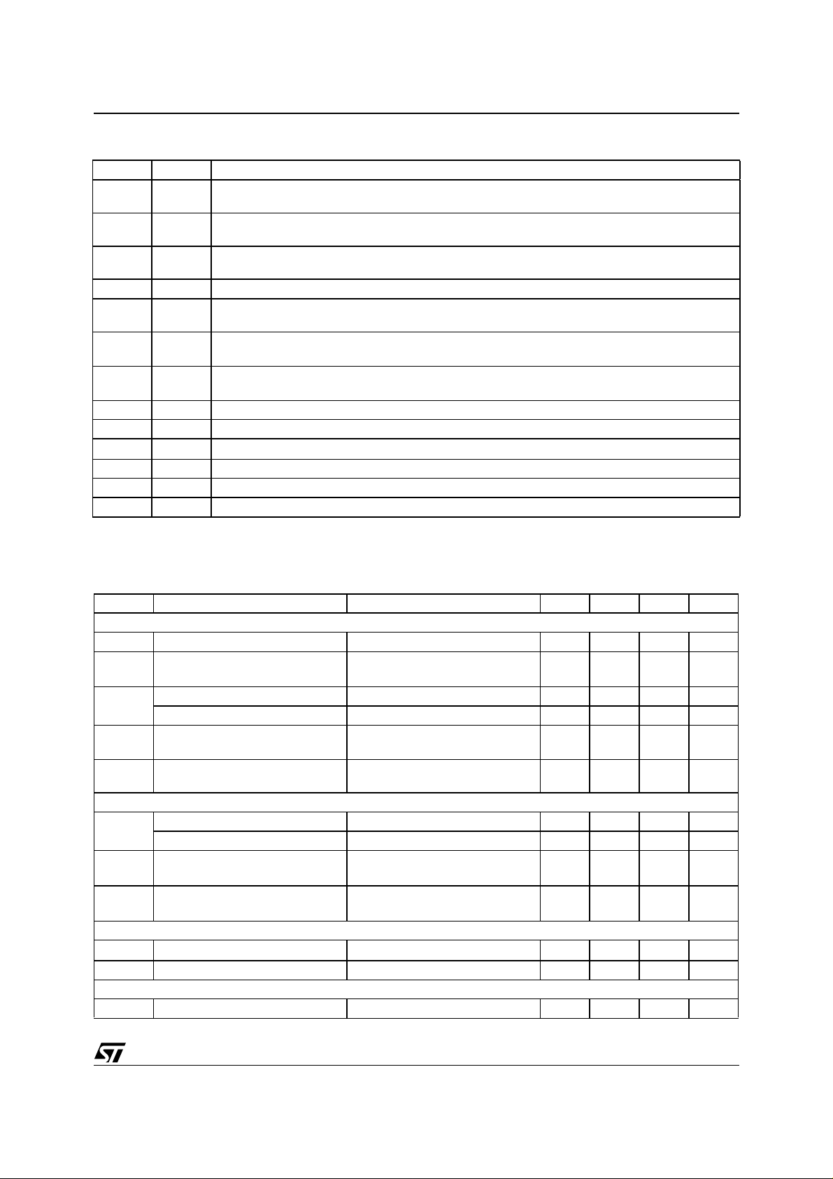
Figure 1. Funct i on a l & Blo c k D iag ram
IN
V
5V
L6995
OUT
V
GNDVCCOVPPGOODSHDN
overvoltage comparator
VSENSE
+
1.15 VREF
-+undervoltage comparator
VSENSE
0.69 VREF
pgood comparators
SR
LS and HS anti-cross-conduction comparators
1.10 VREF
VSENSE
-
+
comp
V(LGATE)<0.5V
VSENSE
+
BOOT
VCC
0.89 VREF
-
HGATE
HS driver
level shifter
V(PHASE)<0.2V
RQ
comp
S
Toff min
PHASE
delay
VDR
Ton min
one-shot
PGND
LGATE
LS driver
Q
R
S
Ton
one-shot
OSC
VSENSE
Ton= Kosc V(VSENSE)/V(OSC)
Q
R
S
mode
no-skip
-
+
PHASE
zero-cross comparator
LS control
Ton
one-shot
OSC
VSENSE
mode
no-skip
Ton= Kosc V(VSENSE)/V(OSC)
NOSKIP
IC enable
control
soft-start
SS
5 uA
power management
ILIM
comparator
positive current limit
-
PHASE
+-+
+VREF
0.2
FB
HS control
VREF
pwm comparator
+
+
-
-
Gm
VREF
INT
VSENSE
SENSEGND
IN
V
OSC
1.236V
bandgap
VREF
1.416
Reference chain
0.9V
5/25

L6995
1 DEVICE DESCRIPTION
1.1 Constant On Time PWM topology
Figure 2. Loop block schem atic diagr am
Vin
R1
R2
One-shot generator
OSC
Vsense
Vref
FFSR
Q
R
HGATE
S
Q
+
LGATE
HS
LS
Vout
DS
-
PWM comparator
FB
R4
R3
The device implements a Constant On Time control scheme, where the Ton is the high side MOSFET on time
duration forced by the one-shot generator. The on time is directly proportional to VSENSE pin voltage and inverse to OSC pin voltage as in Eq1:
V
SENSE
Eq 1
where K
T
ON
= 250ns and τ is the internal propagation delay time (typ. 70ns). The system imposes in steady
OSC
state a minimum on time corresponding to V
responding Ton will not decrease. Connecting the OSC pin to a voltage partition from V
steady-state switching frequency F
== =
Eq 2
f
SW
K
OSC
V
OUT
-------------- -
V
IN
--------------------- -
V
OSC
1
---------- -
T
ON
τ+=
= 2V. In fact if the V
OSC
independent of VIN. It results:
SW
α
OSC
--------------
α
OUT
1
-------------- -
→ fSWK
K
OSC
α
OSC
OSC
OSCαOUT
voltage increases above 2V the cor-
to G N D, it a l lows a
IN
where
V
Eq 3
Eq 4
α
OSC
α
OUT
OSC
-------------- -
V
IN
V
FB
-------------- -
V
OUT
The above equations allow setting the frequency divide r ratio
such equations hold only if V
independent from the input voltage. The delay introduces a light dependenc e from V
R
2
--------------------==
R2R1+
R
4
--------------------==
R3R4+
α
once output voltage has been set; note that
<2V. Further the Eq2 shows how the system h as a sw itching frequenc y ideall y
OSC
OSC
. A minimum off-time con-
IN
strain of about 580ns is introduced in order to assure the boot capacitor charge and to limit the switching fre-
6/25
L6995
quency after a load transient as well as to mask PWM comparator output against noise and spikes.
The system has not an internal clock, b ecause this is a hysteretic control ler, so the turn on puls e will start if three
conditions are met contemporarily : the FB pin voltage i s low er than the refere nce voltage, the minimum o ff time
is passed and the current limit comparator is not triggered (i.e. the inductor current is below the current limit
value). The voltage on the OSC pin must range between 50mV and 2V to ensure the system linearity.
1.2 Closing the loop
The loop is closed connecting the output voltage (or the output divider middle point) to the FB pin. The FB pin
is linked internally to the comparator negative pin and the positive pin is connected to the reference voltage
(0.9V Typ.) as in Figure 2. When the FB goes lower than the reference voltage, the PWM comparator output
goes high and sets the flip-flop outpu t, turning on the hig h side MOSFET. This condition i s latched to av oid noise
spike. After the on-time (calculated as descr ibed in the previous section) the system resets the flip-flop and then
turns off the high side MOSFET and turns on the low side MOSFET. Internally the device has more complex
logic than a flip-flop to manage the transition in correct way. For more details refers to the Figure 1.
The voltage drop along ground and supply metals connecting output capacitor to the load is a source of DC
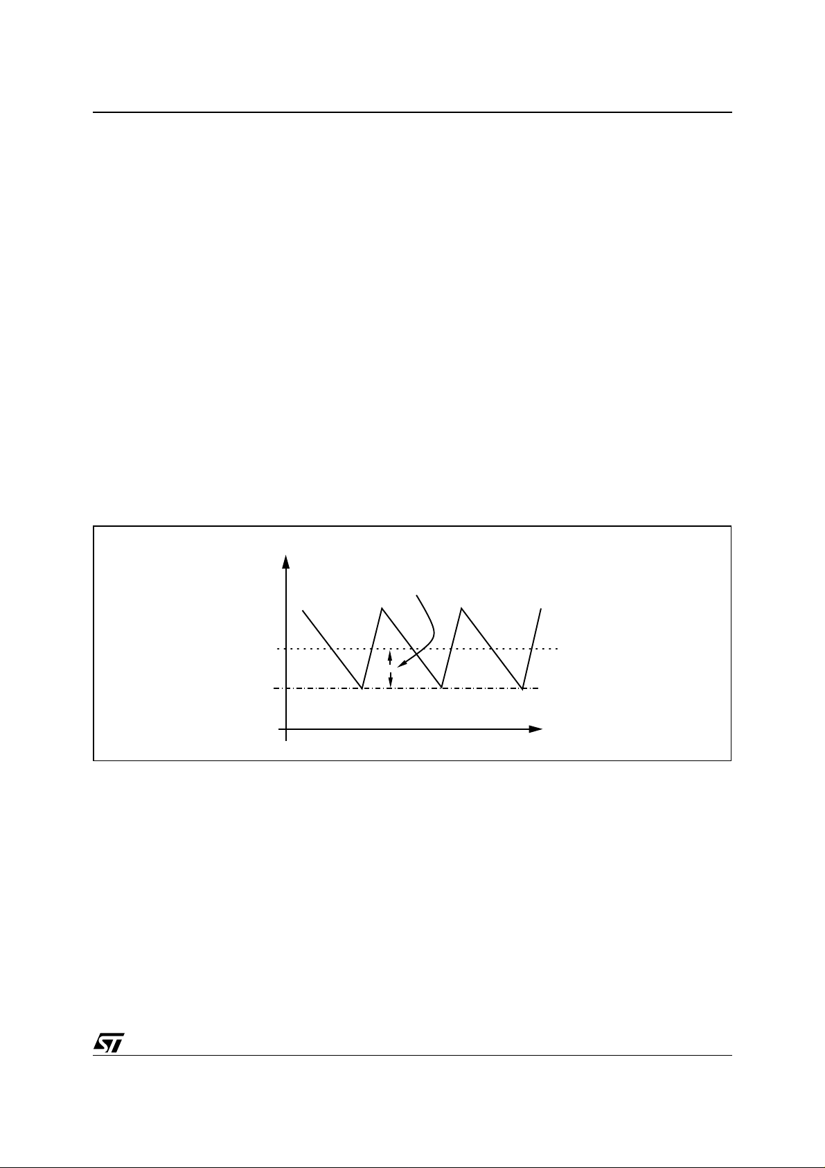
error. Further the system r egulates the o utput voltage v alley v alue not the aver age, as in the Fi gure 3 is show n.
So the voltage ripple on the output capacitor is a source of DC static error (as the PCB traces). To compensate
the DC errors, an integrator network must be introduced in the control lo op, by connectin g the output voltage to
the INT pin through a capacitor and the FB pin to the INT pin directly as in Figure 4. The internal integrator amplifier with the exter nal capac itor C
for output ripple.
introduces a D C pole i n the contr ol l oop. C
INT1
also provides an AC path
INT1
Figure 3. Valle y regulation
Vout
DC Error Offset
<Vout>
Vref
Time
The integrator amplifier generates a current, proportional to the DC errors, that increases the output capacitance
voltage in order to c ompensate the total static err ors. A v oltage clamper within the devi ce fo rces INT pi n v oltage
ranges from V
-50mV, V
REF
+150mV. This is useful to avoid or smooth output voltage overshoot during a load
REF
transient. Also, this means that the integrator is capable of recovering output error due to ripple when its peakto-peak amplitude is less than 150mV in steady state.
In case of the ripple amplitude is larger than 150mV, a capacitor C
can be connected between INT pin and
INT2
ground to reduce r ipple amplitu de at INT pin, otherw ise the integrator can operate out of its linear range. Choose
C
according to the following equation:
INT1
g
⋅
INTαOUT
Eq 5
INT1
where GINT=50 µs is the integrator transconductance,
is the close loop bandwidth. This equation also holds if C
--------------------------------- -=
⋅⋅
2 π F
u
α
is the output divider ratio given from Eq4 and F
OUT
is connected between INT pin and ground. C
INT2
INT2
is given by:
U
7/25

L6995
C
Eq 6
Where
INT2
--------------- -
C
INT1
∆
V
is the output ripple and ∆V
OUT
V
∆
OUT
------------------=
V
INT
INT
Figure 4. Integrator loop block diagram
Vin
R1
R2
Cint2
One-shot generator
OSC
From Vsense
Vref
FB
INT
Integrator amplifier
+
-
PWM comparator
+
is the ripple wanted at the INT pin (100mV typ).
PCB TRACES
FFSR
Q
R
HGA TE
S
Q
LGA TE
Vref
-
-
+
Vsense
Gndsense
HS
LS
DS
Vout
LOAD
Cint1
Respect to a traditional PWM controller, that has an internal osci llator setting the sw itchi ng frequency, in a hysteretic system the frequency can change with some parameters (input voltage, output current). In L6995 is implemented the voltage feed-forward circuit that allows constant switching frequency during steady-sate
operation with the input voltage variation. There are many factors affecting switching frequency accuracy in
steady-state operation. Some of these are internal as dead times, which depend on high side MOSFET driver.
Others related to the external components as high side MOSFET gate charge and gate resistance, voltage
drops on supply and ground rails, low side and high side RDSON and inductor parasitic resistance.
During a posi tive load trans ient, (the output current increases), the converter switches at its maxi mum frequency
(the period is TON+TOFFmin) to recover the output voltage drop. During a negative load transient, (the output
current decreases), the device stops to switch (high side MOSFET remains off).
1.3 Tran si t ion from PWM to PFM/PSK
To achieve high efficiency at light load condition s, PFM mode is provided. The PFM mode differs from the PWM
mode essentially for the off section; the on section is the same. In PFM after a turn-on cycle the system turnson the low side MOSFET, until the inductor current reaches the zero A value, when the zero-crossing comparator turns off the low side M OSFET. In this w ay the energy stor ed in the outp ut capaci tor wi ll not flow to gr ound,
through the low side MO SFET, but it w ill flow to the load. In PWM mode, after a turn on cy cle, the sy stem k eeps
the low side MOSFET on until the next turn-on cycle, so the energy stored in the output capacitor will flow
through the low side MOSFET to ground. The PFM mode is naturally implemented in hysteretic controller, in
fact in PFM mode the system reads the output vol tage with a comparator and then tur ns on the hig h side MOSFET when the output voltage goes down a reference value. The device works in discontinuous mode at light
load and in continu ous mode at high l oad. The transi tion fr om PFM to PWM oc curs when load current is around
half the inductor current ripple. This threshold value depends on V
, L, and V
IN
. Note that the higher the in-
OUT
8/25

L6995
ductor value is, the smaller the threshold is. On the other hand, the bigger the inductor value is, the slower the
transient response is. In PFM mode the frequency changes, with the output current changing, more than in
PWM mode; in fact if the output current increase, th e output v oltage dec reases mor e quickl y; so the suc cessi ve
turn-on arrives before, increasing the switching frequency. The PFM waveforms may appear more noisy and
asynchronous than normal operation, but this is normal behaviour mainly due to the very low load. If the PFM
is not compatible with the application it can be disabled connecting to V
1.4 Softstart
If the supply v oltages are already applied , the SH DN pin gives the start-up. The sys tem s tarts with the high s ide
MOSFET off and the low side MOSFET on. After the SHDN pin is turned on the SS pin voltage begins to increase and the system starts to switch. The softstart is realized by gradually increasing the cur rent limit threshold to avoid output overvoltage. The active soft start range for the V
increase linearly) starts from 0.6V to 1.5V. In this range an internal current source (5
pacitor on the SS pin; the reference current (for the current limit comparator) forced through ILIM pin is proportional to SS p in voltage and it saturates at 5
µ
A (Typ.) when SS vol tage is close to 1.5V and the maximum current
limit is active. Undervoltage protection is disabled until SS pin voltage reaches 1.5V; instead the overvoltage is
always present (see figure 5).
Once the SS pin voltage reaches the 1.5V value, the voltage on SS pin doesn't impact the system operation
anymore. If the SHDN pin is turned on before the supplies, the correct start-up sequence is the following: first
turn-on the power section and after the logic section (V
CC
pin).
Figure 5. Soft -Start Diagram
the NOSKIP pin.
CC
voltage (where the output current limit
SS
µ
A Typ) charges the ca-
Vss
4.1V
1.5V
0.6V
Ilim current
5
A
µ
Soft-start active range
Time
Maximum current limit
Time
Because the system implements the soft start controlling the inductor current, the soft start capacitor selection
is function of the output capacitance, the current limit and the soft start active range (
∆
VSS).
In order to select the softstart capacitor it must be imposed th at the output voltage reaches the final v alue before
the soft start voltage reaches the under voltage value (1.5V). In other words the output voltage charging time
has to be lower than the uvp time.
The UVP time is given by:
V
uvp
Eq 7
T
()
uvpCSS
------------
Iss
⋅=
C
SS
In order to calculate the output volatge chargin time it should be calculated, before, the output volatrge function
versus time. Thi s function c an be calc ulated from the inductor curr ent functi on; the induct or cur rent fu nction can
9/25

L6995
be supposed linear function of the time.
Eq 8
t,CSS()
I
L
R
ilim/RdsonKCISS
--------------------------------------------------------------------------- -=
V
CSS⋅∆()
SS
t⋅⋅⋅()
so the output voltage is given by:
2
t
2⋅⋅∆⋅()
Eq 9
calling V
Eq 10
V
out
as the V
out
I
outCSS
the minimum C
Eq 11 T
out
Qt,C
()
t,CSS()
final value, the output charging time can be estimated as:
out
()
value is given imposing this condition:
SS
=T
uvp
-------------------------------------------------------------------------------------- -
=
SS
------------------------ -
C
out
V
outCout
R
ilim/RdsonKCISS
R
ilim/RdsonKCISS
------------------------------------------------------------------------------ -==
C
out
V
SSCSS
⋅⋅()
⋅⋅⋅()
V
SSCSS
0.5
2⋅⋅∆⋅⋅()
1.5 Current limit
The current limit comparator senses the inductor current through the low side MOSFET RDSON drop and compares this value with the ILIM pin voltage value. While the current is above the current limit value, the control
inhibits the one-shot start.
To properly set the current limit threshold, it should be noted that this is a valley current limit. Average current
depends on the inductor value, V
IN VOUT
and switching frequency.
The average output current in current limit is given by:
Eq 12
I
OUT
CL
I
max valley
I∆
-----+=
2
Thus, to set the current threshold, choose RILIM according to the following equation:
R
ILim
Eq 13
Where K
I
max valley
is the current limit factor (Typ 1µA). In current limit the system keeps the current constant until the
C
-----------------
Rds
on
K
⋅=
C
output voltage meets the undervolatge thr eshold. The sy stem is capable to s ink curre nt, but it has n ot a negative
current limit.
The system accuracy is function of th e exactness of the resistance connecte d to ILIM pin and the l ow side MOSFET RDS
accuracy. Moreover the voltage on ILIM pin must range between 10mV and 2V to ensure the sys-
ON
tem linearity.
Figure 6. Current limit schematic
To inductor
LS
PGN
R
ILIM
Positive current limit
D
Comparator
5µA
PHASE
Current
To
logic
10/25

L6995
1.6 Protection and fault
Sensing VSENSE pin voltage performs output protection. The nature of the fault (that is, latched OV or latched
UV) is given by the PGOOD and OVP pins. If the output voltage is between the 89% (typ.) and 110% (typ) of
the regulated value, PGOOD is high. If a har d overv oltage or an undervoltage occurs, the device is l atched: low
side MOSFET is turned on, high side MOSFET is turned off and PGOOD goes low. In case the system detects
an overvoltage the OVP pin goes high.
To recover the functionality the device must be shut down and restarted thought the SHDN pin, or the supply
has to be removed, and restart with the correct sequence.
These features are useful to protect against short-circuit (UV fault) as well as high side MOSFET short (OV
fault).
1.7 Drivers
The integrated high-current dri vers allow us ing different size of power MOSFET, maintaining fast s witching transition. The driver for the high side MOSFET uses the BOOT pin for supply and PHASE pin for return (floating
driver). The driver for the low side MOSFET uses the VDR pin for the supply and PGND pin for the return. The
main feature is the adaptive anti-cross-conduction protection, which prevents from both high side and low side
MOSFET to be on at the sam e time, avoidi ng a hi gh current to flow from V IN to GN D. Wh en high side MOSFET
is turned off the voltage on the pin PHASE begins to fall; the low side MOSFET is turned on only when the voltage on PHASE pin reaches 250mV. When low side is turned off, high side remains off until LGATE pin voltage
reaches 500mV. This is important since the driver can work pr operly with a l arge range of external pow er MOSFETS.
The current necessary to switch the external MOSFETS flows through the device, and it is proportional to the
MOSFET gate charge and the switching fr equency. So the pow er dissipati on of the devic e is functi on of the external power MOSFET gate charge and switching frequency.
Eq 14
P
driver
V
⋅⋅=
ccQgTOTFSW
The maximum gate charge values for the low side and high side are given from:
f
SW0
Eq 15
Eq 16
Where f
Q
MAXHS
Q
MAXLS
= 500Khz. The equations above are valid for TJ = 150°C. If the system temperature is lower the Q
SW0
------------ -
f
SW
f
SW0
------------ -
f
SW
75nC⋅=
125nC⋅=
can be higher.
For the Low Side driver the max output gate charge meets another limit due to the internal traces degradation;
in this case the maximum value is Q
MAXLS
= 125nC.
The low side driver has been designed to have a low resistance pull-down transistor, around 0.5 ohms. This
prevents the voltage on LGATE pin raises during the fast rise-time of the pin PHASE, due to the Miller effect.
2 APPLICATION INFORMATION
2.1 20A Demo board description
The demoboard shows the device operation in general purpos e applications. The evaluation board all ows using
only one supply because the on board linear regulator LM317LD; the linear regulator supplies the device
through the J1. Output current in excess of 20A can be reached dependently on the MOSFET type. The SW1
is used to start the device (when the supplies are already present) and to select the PFM/PWM mode.
G
11/25

L6995
V
Figure 7. Demoboard Sche m ati c Diagram
5
V
J1
R1
R2
LM317LD
C1
IN
C2
C3
R6 R7
C21
C20
R12
5V
R5
C22
PGOOD
OVP
ILIM
R8
SS
SHDN
2.2 Jumper Connection
VDR
VCC
L6995
C5
R4
OSC
BOOT
HGATE
PHASE
LGATE
PGND
GND
NOSKIP
VSENSE
GNDSENSE
INT
VFB
VREF
R3
With Int.
Q1,2,3,
Q4,5,6
Without Int.
Without Int.
C6
C7
R11
C4
C13,14,15,16,17,18
D1
C19
L
D2
R9
C7,8,9,10,11,12
Vout
LOAD
R10
5V
R13
C23
With Int
Rn
Rn
C24
Table 1. Jumper connection with integrator
Component Connection
C4 Mounted
C7 Mounted *
INT Close
NOINT Open
* This comp onent is not necessary, depends from t he output ESR capacitor. See the integ rator section.
Table 2. Jumper connection without integrator
Component Connection
C4 Not mounted
C7 Not Mounted
INT Open
NOINT Close
12/25

L6995
2.3 NOTE
There is a linear regulator on board, it allows to use one generator (only for the power section, in fact the IC
section is powered by the linear regulator); if the regulator is used close the J1, other wise it has to keep open.
Be careful measuring the efficiency with the linear regulator asserted.
At high current in the integrator configuration (around 20A), it can be seen an oscillation in the switching frequency due to the noise interaction, to reduce this oscillation put a noise filter R
the R
resistor is in the place of the INT jumper near C4. RN, CN, should be selected with a pole frequency
N
around 1Mhz, but anyway higher than switching frequency (five times).
2.4 DEMOBOARD LAYOUT
Real dimensions: 5,7 cm X 7,7 cm (2,28inch X 3, 08inch)
, CN like in the figure 7. Note
N
Figure 8. PCB layout: bottom side
Figure 9. PCB Layout: To p side
Figure 10. Int ernal ground pl a n e
Figure 11. Power & signal plane
13/25

L6995
Table 3. PCB Layout guidelines
Goal Suggestion
Low radiation and low magnetic coupling
with the adjacent circuitry.
Don’t penalty the efficiency. Keep power traces and load connections short and wide.
Ensure high accuracy in the current sense
system.
Reduce the noise effect on IC. 1) Put the feedback component (like output divider, integrator network,
1) Small switching current loop areas. (For example placing C
Side and Low side MOSFETS, Shottky diode as close as possible).
2) Controller placed as close as possible to the power MOSFET.
3) Group the gate drive component (Boot cap and diode together near
the IC.
Phase pin and PGND pin must be made with Kelvin connection and as
close as possible to the Low Side MOSFETS.
etc) as close as possible to the IC.
2) The feedback traces must be parallel and as close as possible.
Moreover they must be routed as far as possible from the switching
current loops.
3) Make the controller ground connection like the figure 19.
, High
IN
Table 4. Component list
The component lis t is sh ared in two secti ons: the firs t for the gener al-purpos e comp onent, the second for power
section:
GENERAL-PURPOSE SECTION
Part name Value Dimension Notes
RESISTOR
R1 100Ω 0603 Output resistor divider for the
linear regulator.
R2 300Ω 0603
R3 560kΩ 0603 Input resistor divider
R4 33kΩ 0603
R5 47Ω 0603
R6, R7, R11, R12 33kΩ 0603
R8 47kΩ 0603 Current limit resistor
R9 390Ω 0603 Output resistor divider
R10 1KΩ 0603
R13 220 Ω 0603
CAPACITOR
C1 220nF 0805
C2 47µF KEMET-16V
C3 220nF 0805
C4 330pF 0603 First integrator capacitor
C5 47pF 0603
C6 10nF 0603
C7 N.M. 0603 Second integrator capacitor
C19 220nF 0805
C20 220nF 0603 Softstart capacitor
(To set switching frequency)
(To set current limit)
(To set output voltage)
14/25

Part name Value Dimension Notes
C21 47pF 0603
C22 220nF 0805
C23 0603 N.M.
C24 1nF 0603
C25 1uF Tantalum
DIODES
D1 BAT54 25V
POWER SECTION
OUTPUT CAPACITORS
C10-C11-C12 3X330uF EEFUE0D331R
PANASONIC
INPUT CAPACITORS
C13, C14, C16, C17,
C15 C18
10uF C34Y5U1E106Z
TOKIN
10uF C3225Y5V1E106Z
TDK
Part name Value Dimension Notes
10uF ECJ4XF1E106Z
PANASONIC
10uF TMK325F106ZH
TAIYO YUDEN
INDUCTOR
L1 0.6µH ETQP6F0R6BFA
PANASONIC
0.6µH A959ASR60N
TOKO
0.6µH DXM1306-R60-T COEV
0.6µH CEP12D38H0R6 SUMIDA
POWER MOS
Q1,Q2 STS 11NF 3LL STM icroe lectro nics Q3 N.M.
STSJ25NF3LL STMicroelectro nics Q3 N.M.
Q5,Q6 STS25NH3LL STMicroelectro nics Q4 N.M.
DIODES
D2 STP S3L4 0U STM icroe lectro nics 25V
INTEGRATED CIRCUIT
U1 LM317L D Linear regulator
U2 L6995
Switcher
Notes: 1. N.M.=Not Mount ed
2. The demoboard wi th this component lis t is set to give: V
the integrator feature, and wit h 20A continu os output current.
3. All capacitors are intended ceramic type otherwise specifi ed.
= 1.25V, FSW = 270kHz wi t h an input vol tage around VIN = 20V with
OUT
Output capacitor C8, C9 N.M.
L6995
Input capacitor
15/25

L6995
3 STEP BY STEP DESIGN
VIN = 20V V
In this design it is considered a low profile demoboard, so a great attention is given to the components height.
3.1 Input capacitor.
A pulsed current (with zero average value) flows through the input capacitor of a buck converter. The AC component of this current is quite high and dissipates a considerable amount of power on the ESR capacitor:
Eq 17
The I
RMS
= 1.25V I
P
OUT
CIN
ESR
OUT
CIN
current is given by:
= 20A FSW = 270kHz
2 Vin Vin Vout–()⋅
⋅⋅=
Iout
-------------------------------------------------- -
Vin
2
δ
Eq 18
Icin
rms
Iout2δ 1 δ–()
------
+=
12
2
∆()
I
L
Neglecting the last term, the equation reduces to:
Eq 19
Icin
rms
which maximum value corresponds to
ICIN
, has a maximum equal to δ = 1/2 (@ VIN = 2×VOUT, that is, 50% duty cycle). The input capacitor,
RMS
therefore, should be selected with an RMS rated current higher than ICIN
Iout δ 1 δ–()=
δ
= 1/2.
. Electrolytic capacitors are the
RMS
most used because are the cheapest ones and are availabl e with a wide range of RMS current ratings. The only
drawback is that, considering a requested ripple curr ent rating, they are physicall y larger than other capacitors.
Very good tantalum capacitors are coming av ailable, with very low ESR and smal l size. The only problem is that
they occasionally can burn out i f subjected to very high current dur ing the charge. So, it is better avoid this type
of capacitors for the input filter of the device. In fact, they can be subjected to high surge current when connected
to the power supply. If available for the requested value and vol tage rating, the cer amic capacitor s hav e usuall y
a higher RMS current rating for a given physical size (due to the ver y low ESR). From the equati on 18 it is found:
Icin
= 4.8A
rms
µ
Considering 10
F capacitors ceramic, that have ICIN
=1.5A, 6 pzs. are needed.
RMS
3.2 Inductor
In order to determine the inductor value is necessary considering the maximum output current to decide the inductor current saturation. Once the inductor current saturation it is found automatically is found the inductor value. In our design it is considered a very
low profile
inductor.
µ
L = 0.6
H
The saturation current for this choke is around 25A
3.3 Output capacitor
The output capacitor is c hosen by the output v oltage static and dynamic accuracy. The static accuracy is related
to the output voltage ripple value, while the dynamic accuracy is related to the output current load step.
If the static precision is around ± 2% for the 1.25V output, the output accuracy is ±25mV.
To determine the ESR value from the output precision is necessary before calculate the ripple current:
16/25

L6995
Vin Vo–
Eq 20
I∆
---------------------- -
L
Vo
-------- -
⋅⋅=
Vin
T
sw
Considering a switching frequency around 270kHz from the equation above the ripple current is around 7A.
So the maximum ESR should be:
∆
V
ripple
Eq 21
ESR
-------------------- - 7mΩ==
I∆
---- -
2
The dynamic specific ations are somet imes mor e relax ed than the static requir ements so the ESR value ar ound
7m
Ω
should be enough.
The current ripple flows through the output ca pacitor , so the output capa citors s hould be c alculated also to sustain this ripple: the RMS current value is given from Eq22.
1
---------- -
I
Eq 22
Icout
rms
23
∆=
L
But this is usually a negligible constrain when choosing output capacitor.
To allow the device control loop to work properly output capacitor zero should be at the least ten times smaller
than switching freq uency. The output capac itor val ue (C
) and the output capacitor E SR (ESR
OUT
) should be
OUT
large enough and small enough, to keep the output voltage ripple within the specification and to give to the device a minimum signal to noise ratio.
3.4 Power MOSFETS and Schottky Diodes
Since a 5V bus powers the gate drivers of the device, the use of logic-level MOSFETS is highly rec ommended,
especially for high current applications. The breakdown voltage VBR
must be greater than VIN
DSS
MAX
with a
certain margin, so the selection will address 20V or 30V devices.
The RDS
can be selected once the allowable power dissipation has been established. By selecting identical
ON
Power MOSFET for the main switch and the synchronous rectifier, the total power they dissipate does not depend on the duty cycle. Thus, if P
RDS
Eq 23
(@ 25 °C) can be derived from:
ON
RDS
ON
----------------------------------------------------- -=
is this power loss (few percent of the rated output power), the required
ON
P
ON
Iout21 α T∆⋅+()⋅
α
is the temperature coefficient of RDSON (typically, α = 510-3 °C-1 for these low-voltage classes) and ∆T the
admitted temperature rise. It is worth noticing, however, that generally the lower RDS
charge Q
, which leads to a higher gate drive consumption. In fact, each switching cycle, a charge QG moves
G
, the higher is the gate
ON
from the input source to ground, resulting in an equivalent drive current:
Eq 24
Iq Qg F
⋅=
SW
The SCHOTTY diode placed in par allel to the synchr onous rectifier mus t have a r everse v oltage VRRM greater
than VIN
. For application with low Duty Cycle, where the input voltage is high (around 20V) it is very impor-
MAX
tant to select the high si de MOSFET with low gate ch arge, to reduce the sw itchi ng loss es as STS 11NF3LL. For
the low side section should be selected a low RDS
as STS25NH3LL.
ON
3.5 Output voltage setting
To select the output divider network there is n't a specific cri t eria, but a low divider network value ( around 100Ω)
reduces the efficiency at low current; instead a high value divider network (500K
Ω
) increase the noise effects.
A network divider values from 1K to 50K is right. From the Eq4:
17/25

L6995
R10 = 1K
R9 = 390
Ω
Ω
The device output voltage is adjustable by connecting a voltage divider from output to VSENSE pin. Minimum
output voltage is V
OUT
= V
= 0.9V. Once output divider and frequency divider have been desi gned as to ob-
REF
tain the required output v oltage and sw itching frequency, the following equation gives the smallest input voltage,
which allows L6995 to regulate (which corresponds to T
Eq 25
δ 1
where the K
α
OSC
--------------
α
OUT
OSC/TOFFMIN
⋅–<
1
----------------------------- -
K
OSC
----------------------- -
T
OFFMIN
ratio worst-case is given in electrical characteristic table (pag. 4).
OFF
= T
OFF, MIN
):
3.6 Voltage Feed Forward
Choosing the switching frequenc y around 270K Hz from the Eq1. It c an be selec ted the input div ider. For example:
R3=560K
R4=28K
Ω
Ω
In order to compensate the comparator delay R4 resistor should be increased around 20%.
R4=33K
Ω
3.7 Current limit resistor
From the Eq13 can be set the valley current limit, knowing the low side RDSON. To set the exact current limit it
must be considered the temperature effect. So two STS25NH3LL have 2.75m
sidered 3.85m
R8 = 47K
Ω
.
Ω
Ω
@ 25°C, at 100°C can be con-
3.8 Integrator capacitor
Let it be FU = 15kHz.
Since VREF = 0.9V, fr om Eq4, i t fol lows
= 0.72 and, from Eq5 i t fol lows C
OUT
= 330pF. Because the ripple
INT1
α
is lower than 150mV the system doesn't need the second integrator capacitor.
3.9 Soft start capacitor
Considering the soft start equations can be found:
= 200pF
C
SS
These equations are valid whitout load. When an active load is present the equantions result more complex;
further some active loads have unexpected effect, as higher current than the expected one during the start up,
that can change the start up time.
In this case the capacitor value can be selected on the application; anyway the Eq11 gives an idea about the
C
value.
SS
18/25

3.9.1 Efficiency
VIN = 20V V
= 1.25V FSW = 270KHz
OUT
Figure 12. Efficiency vs output current
Eff [%]
85
80
75
70
65
60
0,0 4,0 8,0 12,0 16 ,0 20,0 24,0
Vin=20V Vout=1.25V Fsw =220Khz PFM Vin=20V Vout=1.25V Fsw =220Khz PWM
L6995
Cu r r e nt [A]
3.10 5A demo Board
Figure 13. Schematic Diagram
R7
C10
C11
R5
TP1
TP2
R9
SD
R10
PGOOD
OVP
ILIM
R8
C12
SS
C9
SHDN
VCC
VDR
L6995
U1
VSENSE
GNDSENSE
C8
R4
OSC
BOOT
HGA TE
PHASE
LGA TE
PGND
GND
NOSKIP
INT
VFB
VREF
Vcc
R6
C4
Q1
Q2
NOINT
NOINT
C6
TP3
C5
INT
C7,C13
GNDin
D1
L1
R1
D2
C1
C2
NS
Cn
C14,C15
C3
INT
Rn
J1
VIin
VOUT
R3
R2
GNDOUT
19/25

L6995
3.11DEMOBOARD LAYOUT
Real dimensions: 4.7 cm X 2.7 cm (1.85inch X1.063inch)
Figure 14. Top side components placeme nt
Figure 15. Bottom side Jumpers distribution
Figure 16. Top side layout
Figure 17. Bottom side layout
Table 5. Component list
GENERAL-PURPOSE SECTION
Part name Value Dimension Notes
RESISTOR
R1, R5, R9, R10 33kΩ 0603 Pull-up resistor
R2 10kΩ 0603 Output resistor divider
R3 10kΩ 06 03
R4 21kΩ 0603 Input resistor divider
R6 470kΩ 0603
R7 47Ω 0603
R8 120kΩ 0603 Current limit resistor
CAPACITOR
C1 330pF 0603 First integrator capacitor
C2 N.M. 0603 Second integrator capacitor
C3 N.M. 0603 N.M.
C4 100nF 0603
C5 1µF Tantalum
C6 10nF 0603
C8, C12 47pF 0603
C9 22nF 0603 Softstart capacitor
(To set output voltage)
(To set switching frequency)
20/25

Part name Value Dimension Notes
C10 100nF 0603
C11 100nF 0603
DIODE
D1 BAR18
POWER SECTION
INPUT CAPACITORS
C7, C13 10µF C34Y5U1E106ZTE12 TOKIN
OUTPUT CAPACITORS
C14, C15 330µF EEFUE0 D331 R
PANAS ONIC
INDUCTOR
L1 2.7µH DO3316P-272 HC
COILCRAFT
2.2µH ETQP6H2R2G F
PANAS ONIC
3.3µH DQ7545
COEV
POWER MOS
Q1,Q2 STS8DNF3LL STMicroelectronics Double mos in sigle package
DIODE
D2 STPS3L40U STMicroelectronics
Notes: 1. N.M.=Not Mount ed
2. The demobo ard with this co m ponent l i st is set to give: V
with the i ntegrator feature.
3. The diode efficiency impact is very low; it is not a necessary component.
4. All capacitors are intended ceramic type otherwise specifi ed.
= 1.8V, FSW = 25 0kHz wit h an input voltage around VIN = 20V and
OUT
L6995
3
3.11.1E fficiency
Vin = 20V V
= 1.8V Fsw = 270kHz
out
Figure 18. Efficiency vs output current
Eff [ %]
90
80
70
60
50
40
30
0,0 0,5 1,0 1,5 2,0 2 ,5 3,0 3,5 4,0 4,5 5,0 5,5 6,0
Vin=20V Vout=1.8V Fsw =270Khz PWM Vin=20V Vout=1.8V Fsw =270Khz PFM
Current [A]
21/25

L6995
4 TYPICAL OPERATING CHARACTERISTICS
The measurements refer to the part list in table 4. Vin = 20V V
= 1.25V Fsw = 270kHz T
out
amb
= 25°C.
Figure 19. Soft Start with no load.
Ch1-> Inductor current
Ch2-> Output voltage
Figure 20. Soft Start with 20A load.
Figure 21. Normal functionality in PSK mode.
Ch1-> Inductor current
Ch2-> Output voltage
Ch3-> Phase voltage
Figure 22. Normal functionality in PWM mode.
Ch1-> Inductor current
Ch2-> Output voltage
Ch3-> Soft Start voltage
22/25
Ch1-> Inductor current
Ch2-> Output voltage
Ch3-> Phase voltage

L6995
Figure 23. Load transient from 0 to 18A.
Ch1-> Output current
Ch2-> Output voltage
Ch3->Phase voltage
Figure 24. Load transient from 18A to 0A..
Figure 25. Switching Frequency Vs Output
current
Fsw
[Khz]
350
300
250
200
150
PSK/PFM
PWM
100
50
0
510152025
Vin [V]
Figure 26. Switching Frequency Vs Input
Voltage
Fsw
[Khz]
Ch1-> Output current
Ch2-> Output voltage
Ch3->Phase voltage
350
300
250
200
150
100
50
0
0,0 5,0 10,0 15,0 20,0 25,0
C urrent [ A ]
PFM
PWM
23/25

L6995
DIM.
mm inch
MIN. TYP. MAX . MIN. TYP. MAX.
A 1.20 0.047
A1 0.050 0.150 0.002 0.006
A2 0.800 1.000 1.050 0.031 0 .039 0.041
b 0.190 0.300 0.007 0.012
c 0.090 0.20 0 0.004 0.008
D (1) 6.400 6.500 6.600 0.252 0.256 0.260
E 6.200 6.400 6.600 0.244 0.252 0.260
E1 (1) 4.300 4.400 4.500 0.170 0.173 0.177
e 0.650 0.026
L 0.450 0.600 0.750 0.018 0.024 0.030
L1 1.000 0.039
k 0˚ (min.) 8˚ (max.)
aaa 0.100 0.004
Note: 1. D and E1 d oes no t in clu de mo ld fla sh or p rotru sio ns.
Mold flash or potrusions shall not exceed 0.15mm
(.006inch) per side.
OUTLINE AND
MECH ANICAL DA T A
TSSOP20
Thin Shrink Small Outline Package
24/25
0087225 (Jedec MO-153-AC)

L6995
Information furnished is believed to be accurate and reliable. However, STMicroelectronics assumes no responsibility for the consequences
of use of such information nor for any infringement of patents or other rights of third parties which may result from its use. No license is granted
by implic ation or otherwise under any patent or patent r i ght s of STMi croelectr oni cs. Spec i fications mentioned i n this publication are subject
to change without notice. This publication supersedes and replaces all information previously supplied. STMicroelectronics product s are not
authorized for use as cri tical comp onents in lif e support devi ces or systems without express written approva l of STMicroel ectronics.
The ST logo is a registered trademark of STMicroelectronics
© 2002 STMicroelectronics - All Rights Reserved
Austra lia - Brazil - Canada - Chi na - F i nl and - Franc e - Germany - Hong Kong - In di a - Israel - Ita l y - J apan -Malaysia - Malta - Morocco -
Singap ore - Spain - Sw eden - Switze rl and - Unit ed K i ngdom - United States .
STMicroelectronics GROUP OF COMPANIES
http://www.s t. com
25/25
 Loading...