

HIGH EFFICIENCY MONOLITHIC SYNCHRONOUS
■ 2V TO 5.5V BATTERY INPUT RANGE
■ HIGH EFFICIENCY: UP TO 95%
■ INTERNAL SYNCHRONOUS SWITCH
■ NO EXTERNAL SCHOTTKY REQUIRED
■ EXTREMELY LOW QUIESCENT CURRENT
■ 1µA MAX SHUTDOWN SUPPLY CURRENT
■ 800mA MAX OUTPUT CURRENT
■
ADJUSTABL E OUTPUT VOLTAGE FROM 0.6V
■ LOW DROP-OUT OPERA TION: UP TO100%
DUTY CYCLE
■ SELECTABLE LOW NOISE/LOW
CONSUMPTION MODE AT LIGHT LOAD
■ POWER GOOD SIGNAL
■ ±1% OUTPUT VOLTAGE ACCURACY
■ CURRENT-MODE CONTROL
■ 600kHz SWITCHING FREQUENCY
■ EXTERNALLY SYNCHRONIZABLE FROM
500kHz TO 1.4MHz
■ OVP
■ SHORT CIRCUIT PROTECTION
APPLICATIONS
■ BATTERY-POWERED EQUIPMENTS
■ PORTABLE INSTRUMENTS
■ CELLULAR PHONES
■ PDAs AND HAND HELD TERMINALS
■ DSC
L6926D
STEP DOWN REGULATOR
MSOP8
ORDERING NUMBERS: L6926D
L6926D013TR (Tape & Reel)
■ GPS
DESCRIPTION
The device is dc-dc monolithic regulator specifically
designed to provide extremely high efficiency.
L6926D supply voltage can be as low as 2V allowing
its use in singl e Li-ion c ell supplied applications . Output voltage can be selected by an external divider
down to 0.6V. Duty Cycle can saturate to 100% allowing low drop-out operation. The device is based
on a 600kHz fixed-fr equency, current mode -arc hitecture. Low Consumption Mode operation can be selected at light load conditions, allowing switching
losses to be reduced. L6926D is externally synchronizable with a clock which makes it useful in noisesensitive applications. Other features like Powergood, Overvoltage protection, Shortcircuit protection
and Thermal Shutdown (150°C) are also present.
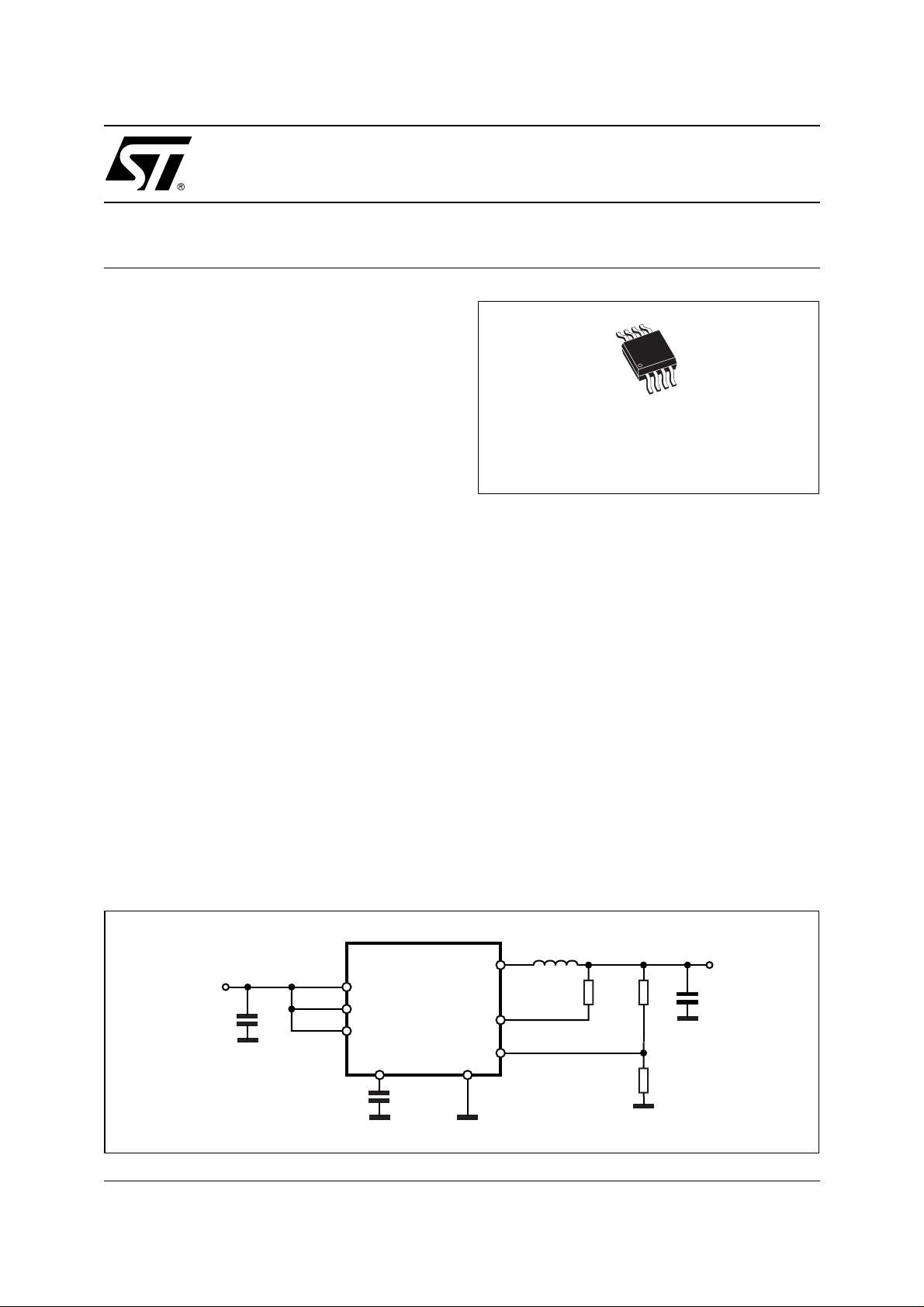
APPLICATION TEST CIRCUIT
May 2003
V
=2V to 5.5V
IN
C1
10µF
6.3V
SYNC LX
D01IN1305
7
V
CC
RUN
6
1
24
COMP GND
C2
220pF
5
8
3
L 6.8µH
PGOOD
VFB
R3
500K
R2
200K
R1
100K
V
=1.8V
OUT
C4
10µF
6.3V
1/8
L6926D
ABSOLUTE MAXIMUM RATINGS
Symbol Parameter Value Unit
V
6
V
5
V
1
V
3
V
2
Ptot Power dissipation at Tamb=70°C0.45W
Tj Junction operating temperature range -40 to 150 °C
Tstg Storage temperature range -65 to 150 °C
LX Pin Maximum Withstanding Voltage Range Test Condition: CDF-
Other pins ±2000 V
PIN CONNECTION
Input voltage -0.3 to 6 V
Output switching voltage -1 to V
Shutdown -0.3 to V
Feedback voltage -0.3 to V
Analog input voltage -0.3 to V
CC
CC
CC
CC
±1000 V
AEC-Q100-002- “Human Body Model” Acceptance Criteria:
“Normal Performance’
V
V
V
V
RUN
COMP
VFB
GND
1
2
3
4LX
D01IN1239AMOD
PGOOD8
SYNC
7
V
6
5
CC
THERMAL DATA
Symbol Parameter Value Unit
R
th j-amb
Thermal Resistance Junction to Ambient 180 °C/W
PIN FUNCTIONS
N Name Description
1 RUN Shutdown input. When connected to a low level (lower than 0.4V) the device stops working.
When high (higher than 1.3V) the device is enabled.
2 COMP Error amplifier output. A compensation network has to be connected to this pin. Usually a
220pF capacitor is enough to guarantee the loop stability.
3 VFB Error amplifier inverting input. The output voltage can be adjusted from 0.6V up to the input
4 GND Ground.
5 LX Switch output node. This pin is internally connected to the drain of the internal switches.
6 VCC Input voltage. The start up input voltage is 2.2V (typ) while the operating input voltage range is
7 SYNC Operating mode selector input. When high (higher than 1.3V) the Low Consumption Mode is
8 PGOOD Power good comparator output. It is an open drain output. A pull-up resistor should be
voltage by connecting this pin to an external resistor divider.
from 2V to 5.5V. An internal UVLO circuit realizes a 100mV (typ.) hysteresis.
selected. When low (lower than 0.5V) the Low Noise Mode is selected. If connected with an
appropriate external synchronization signal (from 500KHz up to 1.4MHz) the internal
synchronization circuit is activated and the device works at the same switching frequency.
connected between PGOOD and VOUT (or VCC depending on the requirements). The pin is
forced low when the output voltage is lower than 90% of the regulated output voltage and goes
high when the output voltage is greater than 90% of the regulated output voltage. If not used the
pin can be left floating.
2/8
L6926D
ELECTRICAL CHARACTERISTICS
(Tj = 25°C, VCC = 3.6V unless otherwise specified)
Symbol Parameter Test Condition Min Typ Max Unit
V
V
cc ON
V
cc OFF
V
cc hys
R
R
I
V
f
f
sync
cc
p
n
lim
out
osc
Operating input voltage After Turn on 2 5.5 V
Turn On threshold 2.2 V
Turn Off threshold 2 V
Hysteresis 100 mV
High side Ron V
Low side Ron V
= 3.6V, I
cc
= 3.6V, I
cc
=100mA 240 mΩ
lx
=100mA 215 mΩ
lx
Peak current limit Vcc = 3.6V 1.2 A
Valley current limit V
Output voltage range V
= 3.6V 1.4 A
cc
fb
Vcc V
Oscillator frequency 600 KHz
Sync mode clock (*) 500 1400 KHz
DC CHARACTERISTICS
I
q
Quiescent current (low noise
mode)
Quiescent current (low
cunsumption mode)
I
sh
I
lx
Shutdown current RUN to GND, V
LX leakage current (*) RUN to GND, V
V
= 0V , no load, VFB >
sync
0.6V
V
= Vcc, no load, VFB
sync
> 0.6V
V
= 5.5V
cc
RUN to GND, V
V
= 5.5V
cc
230 µA
25 µA
= 5.5V 0.2 µ A
cc
LX
LX
= 5.5V,
= 0V,
1 µA
1 µA
ERROR AMPLIFIER CHARACTERISTICS
V
fb
I
fb
Voltage feedback 0.593 0.6 0.607 V
Feedback input current (*) VFB = 0.6V 25 nA
RUN
V
V
run_H
run_L
I
run
RUN threshold high 1.3 V
RUN threshold low 0.4 V
RUN input current (*) 25 nA
SYNC/MODE FUNCTION
V
sync_H
V
sync_L
Sync mode threshold high 1.3 V
Sync mode threshold low 0.5 V
PGOOD SECTION
V
PGOOD
∆V
PGOOD
V
Pgood(low)
I
LK-PGOOD
Power Good Threshold V
Power Good Hysteresis V
Power Good Low Voltage Run to GND 0.4 V
Power Good Leakage Current
OUT
OUT
V
PGOOD
= V
= V
fb
fb
90 %Vout
4%Vout
= 3.6V 50 nA
(*)
PROTECTIONS
HOVP Hard overvoltage threshold V
(*) Guarant eed by design
OUT
= V
fb
10 %Vout
3/8

L6926D
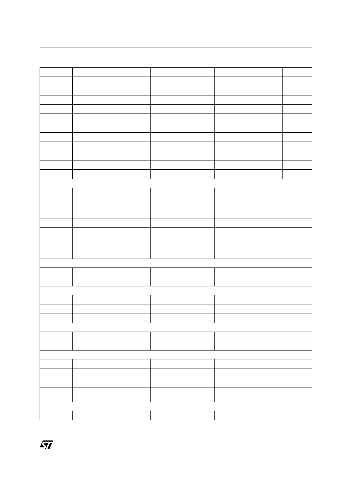
OPERATION DESCRIPTION
The main loop uses slope compensated PWM current mode architecture. Each cycle the high side MOSFET
is turned on, triggered by the oscillator, so that the current flowing through it (the same as the inductor current)
increases. When this current reaches the threshold (set by the output of the error amplifier E/A), the peak current
limit comparator PEAK_CL turns off the high side MOSFET and turns on the low side one until the next clock
cycle begins or the current flowing through it goes down to zero (ZERO CROSSING comparator). The peak inductor current requi red to trigger PEAK_CL depends on the s lope c ompensatio n sig nal and on the output of the
error amplifier.
In particular, the error amplifier output depends on the VFB pin voltage. When the output cur rent increas es, the
output capacitor is dis charged and s o the VF B pin decreases . This pr oduces inc rease of the er ror ampli f ier output, so allowing a higher value for the peak inductor curr ent. For the same reas on, when due to a load trans ient
the output current decreases, the er ror ampl ifier output goes low, so r educi ng the peak inductor c urrent to meet
the new load requirements.
The slope compensation signal allows the loop stability also in high duty cycle conditions (see related section)
Figure 1. Device Block Diagram
RUN
COMP
COMP
SYNC
SYNC
OSCILLATOR
OSCILLATOR
LOW
LOW
NOISE/
NOISE/
CONSUMPTION
CONSUMPT ION
LOOP
E/A
FB
FB
V
V
E/A
REF
REF
0.6V
0.6V
OVP
OVP
LOO P
CONTROL
CONTROL
RUN
PEAK
PEAK
CL
CL
GND
GND
SENSE
SENS E
P
P
MOS
MOS
SLO P E
SLO P E
GND
GND
DRIVER
DRIVER
VCC
VCC
POWER
POWER
P
P
MOS
MOS
LX
LX
ZERO
ZERO
CROSSING
CROSSIN G
GND
GND
VAL L EY
VAL L EY
CL
CL
GND
GND
POWER
POWER
N
N
MOS
MOS
SENSE
SENS E
Vcc
Vcc
Vcc
Vcc
N
N
MOS
MOS
P
P
GOOD
GOOD
P
P
GOOD
0.9V
0.9V
GOOD
V
V
REF
REF
Modes of Operation
Depending on the SYNC pin value the device can operate in low consumption or low noise mode. If the SYNC
pin is high (higher than 1.3V) the low consumption mode is selected while the low noise mode is selected if the
SYNC pin is low (lower than 0.5V).
Low Consumption Mode
In this mode of operation, at light load, the device operates discontinuously based on the COMP pin voltage, in
order to keep the efficiency very high also in these conditions. While the device is not switching the load discharges the output capacitor and the output voltage goes down. When the feedback voltage goes lower than
the internal reference, the COMP pin voltage increases and when an internal threshold is reached, the device
starts to switch. In these conditions the peak current limit is set approximately in the range of 200mA-400mA,
depending on the slope compensation (see related section).
Once the device starts to switch the output capacitor is recharged. The feedback pin increases and, when it
reaches a value slightly higher than the reference voltage, the output of the error amplifier goes down until a
clamp is activated. At this point, the dev ice s tops to switch. In thi s phase, m ost of the internal cir cuitri es are off,
so reducing the device consumption down to a typical value of 25
µ
A.
4/8

L6926D
Low Noise Mode
If for noise reasons, the very low frequenc ies of the low consumpti on mode are undesirable, the low noi se mode
can be selected. In low nois e mode, the effic iency is a l ittle bit lower co mpared with the low consumpti on mode
in very light load conditions but for medium-high load currents the efficiency values are very similar.
Basically, the device switches with its internal free running frequency of 600KHz. Obviously, in very light load
conditions, the device could skip some cycles in order to keep the output voltage in regulation.
Synchronization
The device can also be synchronized with an external signal from 500KHz up to 1.4MHz.
In this case the low noise mode is automatically selected. The device will eventually skip some cycles in very
light load conditions.
The internal synchronization circuit is inhibited in shortcircuit and overvoltage conditions in order to keep the
protections effective (see relative sections).
Short Circuit Protection
During the device operation, the inductor current increases during the high side turn on phase and decrease
during the high side turn off phase based on the following equations:
VINV
–()
∆I
ON
---------------------------------- -
OUT
T
⋅=
L
ON
V
()
OUT
OFF
-------------------
OUT
⋅=
T
OFF
L
can be very close to zero. In this case ∆ION increases
∆I
In strong overcurrent or shortcircuit conditions the V
and
∆
I
decreases. When the inductor peak current reaches the current limit, the high side mosfet turns off
OFF
and so the T
Anyway, if V
T
the current decays very slowly.
OFF
is reduced down to the minimum v alue (250ns typ.) in order to reduce as much as po ssibl e ∆ION.
ON
is low enough it can be that the inductor peak current further increases because during the
OUT
Due to this reason a second protection that fixes the maximu m inductor va lley current has be en introduced. This
protection doesn't allow the high side MOSFET to turn on if the current flowing through the inductor is higher
that a specified threshold (valley current limit). Basically the T
is increased as much as requi re d to bring the
OFF
inductor current down to this threshold.
So, the maximum peak current in worst case conditions will be:
V
IN
---------
I
PEAKIVALLEY
Where IPEAK is the valley current limi t (1.4A typ .) and T
⋅+=
L
ON_MIN
T
ON_MIN
is the minimum TON of the high side MOSFET.
Slope Compensation
In current mode architectures, when the duty cy cle of the application is higher than approxim ately 50%, a pulseby-pulse instability (the so called sub harmonic oscillation) can occur.
To allow loop st ability also in these conditions a sl ope compens ation i s present. Thi s is realized by r educi ng the
current flowing through the induct or neces sary to trigger the COMP c omparator (with a fixed val ue for the COMP
pin voltage).
With a given duty cycle higher than 50%, the stability problem is particularly present with an higher input v oltage
(due to the increased current ripple across the inductor), so the slope compensation effect increases as the input
voltage increases.
5/8

L6926D
From an application point of vi ew, the fi nal effect i s that the peak current limit d epends both on the duty cyc le (if
higher than approximately 40%) and on the input voltage.
Loop Stability
Since the device is realized with a current mode architecture, the loop stability is usually not a big issue. For
most of the application a 220pF connected between the COMP pin and ground is enough to guarantee the stability. In case very low ESR capacitors are used for the output filter, such as multilayer ceramic capacitors, the
zero introduced by the capacitor its elf can shi ft at ver y high frequenc y and the transient loop response c ould be
affected. Adding a series resistor to the 220pF capacitor can solve this problem.
The right value for the r esistor (i n the r ange of 50K) can be deter mined by checking the load transient response
of the device. Basically, the output voltage has to be checked at the scope after the load steps required by the
application. In case o f stabili ty problems , the output vol t age could oscil lates before to reac h the regulated v alue
after a load step.
ADDITIONAL FEATURES AND PROTECTIONS
DROPOUT Operation
The Li-Ion battery voltage ranges from approximately 3V and 4.1V-4.2V (depending on the anode material). In
case the regulated output voltage is from 2.5V and 3.3V, it can be that, close to the end of the battery life, the
battery voltage goes down to the regulated one. In this case the device stops to switch, working at 100% of duty
cycle, so minimizing the dropout voltage and the device losses.
PGOOD (Power Good Output)
A power good output signal is available. The VFB pin is internally connected to a comparator with a threshold
set at 90% of the of reference voltage (0.6V ). Since the output vol tage is c onnected to the V FB pin by a r es istor
divider, when the outp ut voltage goes lo wer than the regulated v alue, the VF B pin v oltage goes lower than 90%
of the internal reference value. The internal comparator is triggered and the PGOOD pin is pulled down.
The pin is an open drain output and so, a pull up resistor should be connected to him.
If the feature is not required, the pin can be left floating.
ADJUSTABLE OUTPUT VOLTAGE
The output voltage can be adjus ted by an exter nal resis tor divider from a m inimum v alue of 0.6V up to the input
voltage. The output voltage value is given by:
R
2
V
OUT
0.6 1
⋅=
------ -+
R
1
OVP (Overvoltage Protection)
The device has an internal overvoltage protection circuit to protect the load.
If the voltage at the feedbac k pin goe s higher than an internal threshold set 10% (typ) higher than the refer ence
voltage, the low side power mosfet is turned on until the feedback voltage goes lower than the reference one.
During the overvoltage circuit intervention, the zero crossing comparator is disabled so that the device is also
able to sink current.
THERMAL SHUTDOWN
The device has also a thermal shutdown protec tion acti vated when the juncti on temper ature reaches 150 C . In
this case both the high side MOSFET and the low side one are turned off. Once the junction temperature goes
back lower than 95 C, the device restarts the normal operation.
6/8

L6926D
DIM.
mm inch
MIN. TYP. MAX. MIN. TYP. MAX.
A 1.10 0.043
A1 0.050 0.150 0.002 0.006
A2 0.750 0.850 0.950 0.03 0.033 0.037
b 0.250 0.400 0.010 0.016
c 0.130 0.230 0.005 0.009
D (1) 2.900 3.000 3.100 0.114 0.118 0.122
E 4.650 4.900 5.150 0.183 0.193 0.20
E1 (1) 2.900 3.000 3.100 0.114 0.118 0.122
e 0.650 0.026
L 0.400 0.550 0.700 0.016 0.022 0.028
L1 0.950 0.037
k 0˚ (min.) 6˚ (max.)
aaa 0.100 0.004
Note: 1. D and F doe s not include mold flash o r protru sions.
Mold flash or potrusions shall not exceed 0.15mm
(.006inch) per side.
OUTLINE AND
MECH ANICAL DA T A
MSOP8
(Body 3mm)
7/8

L6926D
Information furnished is believed to be accurate and reliable. However, STMicroelectronics assumes no responsibility for the consequences
of use of such information nor for any infringement of patents or other rights of third parties which may result from its use. No license is granted
by implic ation or otherwise under any patent or p atent right s of STMicroelectr oni cs. Spec i fications mentioned i n this publication are subje ct
to change without notice. This publication supersedes and replaces all information previously supplied. STMicroelectronics products are not
authorized for use as cri tical comp onents in life support dev i ces or systems wi thout express written approval of STMicroel ectronics.
The ST logo is a registered trademark of STMicroelectronics
2003 STMicroelectronics - All Ri ghts Rese rved
Austra lia - Brazil - Canada - Ch i na - F i nl and - France - Germany - Hong Kong - India - Israel - I taly - Japan -M alaysia - Ma l ta - Morocco -
Singap ore - Spain - Sw eden - Switze rl and - United Kingdom - U n i t ed States.
STMicroelectronics GROUP OF COMPANIES
http://www.s t. com
8/8
 Loading...