


5 BIT PROGRAMMABLE MULTIPHASE CONTROLLER
■
OUTPUT CURRENT IN EXCESS OF 100A
■
ULTRA FAST LOAD TRANSIEN T RESP ONSE
■
REMOTE SENSE BUFFER
■
INTEGRATED 2A GATE DRIVERS
■
5 BIT VID VOLTAGE POSITI ONING, VRM 9.0
■
0.6% INTERNAL REFERENCE ACCURACY
■
DIGITAL 2048 STEP SOFT-START
■
OVP & OCP PROTECTIONS
■
Rdson or Rsense CURRENT SENSING
■
1200KHz EFFECTIVE SWITCHING
FREQUENCY, EXTERNALLY AD JUSTABLE
■
POWER GOOD OUTPUT AND INHIBIT
■
PACKAGE: SO28
APPLICATIONS
■
HIGH DENSITY DC-DC FOR SERVERS AND
WORKSTATIONS
■
SUPPLY FOR HIGH CURRENT
MICROPROCESSORS
■
DISTRIBUTED POWER
L6918 L6918A
SO28
ORDERING NUMBERS: L6918D, L6918AD
L6918DTR, L6918ADTR
DESCRIPTION
L6918A is a master devi ce that it has to be combined
with the L6918,slave, realizing a 4-phases topology,
interleaved. The device kit is specifically designed to
provide a high performance/high densit y DC/DC conversion for high current microprocessors and distributed power. Each device implements a dual-phase
step-down controller with a 180° phas e-shift between
each phase.
A precise 5-bit DAC allows adjusting the output voltage from 1.100V to 1.850V with 25mV binary steps.
The high peak current gate drives affords to have
high system switching frequency, typically of
1200KHz, and higher by external adjustement.
The device kit assure a fast protection against OVP,
UVP and OCP. An internal crowbar, by turning on the
low side mosfets, elimi nates the ne ed of external protection. In case of over-current, the system works in
Constant Current mode.
PIN CONNECTIONS
LGATE1
1
VCCDR
2
PHASE1
3
UGATE1
4
BOOT1
5
VCC
6
SGND
7
COMP
8
FB
9
VPROG_OUT
SYNC_OUT
SLAVE_OK
October 2002
ISEN1
PGNDS1
10
11
12
13
14
L6918A
PGND
28
27
26
25
24
23
22
21
Master)
(
20
19
18
17
16
15
LGATE2
PHASE2
UGATE2
BOOT2
PGOOD
VID4
VID3
VID2
VID1
VID0
OSC / INH / FAULT
ISEN2
PGNDS2
LGATE1
1
VCCDR
2
PHASE1
3
UGATE1
4
BOOT1
5
VCC
6
SGND
7
COMP
8
FB
VSEN
FBR
FBG
ISEN1
PGNDS1
L6918
9
10
11
12
13
14
28
27
26
25
24
23
22
21
(Slave)
20
19
18
17
16
15
PGND
LGATE2
PHASE2
UGATE2
BOOT2
PGOOD
VPROG_IN
SYNC_IN
SLAVE_OK
SYNC / ADJ
SYNC_OUT
OSC / INH / FAULT
ISEN2
PGNDS2
1/35
L6918 L6918A
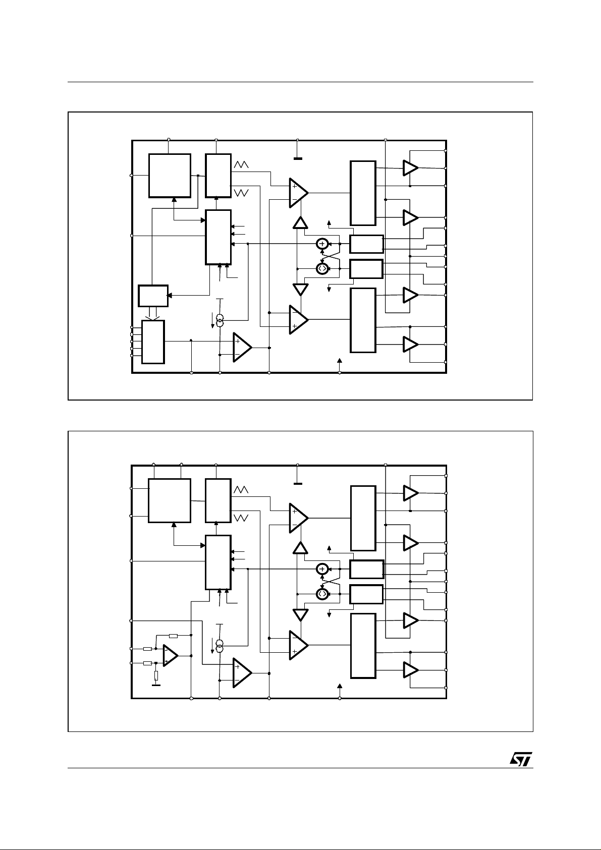
L6918A (MASTER) DEVICE BLOCK DIAGRAM
SYNC_ OU T
SLAVE_OK
SLAVE_OK
PGOOD
PGOOD
VID4
VID4
VID3
VID3
VID2
VID2
VID1
VID1
VID0
VID0
SYNC_ OU T
CIRCUITRY
CIRCUITRY
DIGITAL
DIGITAL
SOFT- START
SOFT- S TAR T
DAC
DAC
SYNC H.
SYNC H.
ROSC / INH SGND VCCDR
ROSC / INH SGND VCCDR
2 PHASE
2 PHASE
OSCILLATOR
OSCILLATOR
VCC
VCC
VCCDR
VCCDR
LOGIC AND
LOGIC AND
PROTECTIONS
PROTECTIONS
CH2 OCP
CH2 OCP
CH1 OCP
CH1 OCP
I
I
FB
FB
ERROR
ERROR
AMPLIFIER
AMPLIFIER
TO TAL
TO TAL
CURRENT
CURRENT
PWM1
PWM1
CURRENT
CURRENT
PWM2
PWM2
BOOT1
BOOT1
HS
HS
LOGIC PWM
LOGIC PW M
LOGIC PW M
ADAPT IVE AN TI
ADAPTI VE AN TI
Vcc
Vcc
ADAPTI VE AN TI
CROS S CO NDU CT I ON
CROS S CO NDU CT I ON
CROS S CO NDU CT I ON
CURRENT
CURRENT
CURRENT
READING
READIN G
READIN G
CURRENT
CURRENT
CURRENT
READING
READING
READING
LOGIC PW M
LOGIC PW M
LOGIC PW M
ADAPTI VE ANTI
ADAPTI VE ANTI
ADAPTI VE ANTI
CROS S CONDU CT ION
CROS S CONDU CT ION
CROS S CONDU CT ION
LS
LS
HS
HS
LS
LS
CH1
CH1
OCP
OCP
CURRENT
CURRENT
COR RECTIO N
COR RECTIO N
AVG
AVG
CH2
CH2
OCP
OCP
CURRENT
CURRENT
COR RECTIO N
COR RECTIO N
VccCOMPFBVSEN
VccCOMPFBVSEN
UGATE1
UGATE1
PHAS E1
PHAS E1
LGATE1
LGATE1
ISEN1
ISEN1
PGNDS1
PGNDS1
PGND
PGND
PGNDS2
PGNDS2
ISEN2
ISEN2
LGATE2
LGATE2
PHAS E2
PHAS E2
UGATE2
UGATE2
BOOT2
BOOT2
L6918 (SLAVE) DEVICE BLOCK DIAGRAM
CIRCUITRY
CIRCUITRY
10k
10k
10k
10k
10k
10k
SYNC_O UT
SYNC_O UT
SYNCH.
SYNCH.
10k
10k
REMOTE
REMOTE
BUF FER
BUF FER
R O SC / IN H SG N D V C C DR
R O SC / IN H SG N D V C C DR
2 PHASE
2 PHASE
OSCILLATOR
OSCILLATOR
VCC
VCC
VCC DR
VCC DR
LOGIC AND
LOGIC AND
PROTECTIONS
PROTECTIONS
CH2 OCP
CH2 OCP
CH1 OCP
CH1 OCP
I
I
FB
FB
ERROR
ERROR
AMPLIFIER
AMPLIFIER
VSEN
VSEN
VSEN
VSEN
SYNC_IN
SYNC_IN
SLAVE_OK
SLAVE_OK
PGOOD
PGOOD
VPROG_IN
VPROG_IN
FBG
FBG
FBR
FBR
SLAVE / ADJ
SLAVE / ADJ
TO TAL
TO TAL
CURRENT
CURRENT
PWM1
PWM1
CURRENT
CURRENT
PWM2
PWM2
BOOT1
BOOT1
HS
HS
LOGIC PW M
LOGIC PW M
LOGIC PW M
ADAPTI VE AN TI
ADAPTI VE AN TI
Vcc
Vcc
ADAPTI VE AN TI
CROSS CONDUCTION
CROSS CONDUCTION
CROSS CONDUCTION
CURRENT
CURRENT
CURRENT
READING
READING
READING
CURRENT
CURRENT
CURRENT
READING
READING
READING
LOGIC PW M
LOGIC PW M
LOGIC PW M
ADAPTI VE ANTI
ADAPTI VE ANTI
ADAPTI VE ANTI
CROSS CONDUCTION
CROSS CONDUCTION
CROSS CONDUCTION
LS
LS
HS
HS
LS
LS
CH1
CH1
OCP
OCP
CURRENT
CURRENT
CORRECTION
CORRECTION
AVG
AVG
CH2
CH2
OCP
OCP
CURRENT
CURRENT
CORRECTION
CORRECTION
VccCOMPFB
VccCOMPFB
UGATE1
UGATE1
PHAS E1
PHAS E1
LGATE1
LGATE1
ISEN1
ISEN1
PGNDS1
PGNDS1
PGND
PGND
PGNDS2
PGNDS2
ISEN2
ISEN2
LGATE2
LGATE2
PHAS E2
PHAS E2
UGATE2
UGATE2
BOOT2
BOOT2
2/35

L6918 L6918A
g
ABSOLUTE MAXIMUM RATINGS
Symbol Parameter Value Unit
Vcc, V
CCDR
V
BOOT-VPHASE
V
UGATE1-VPHASE1
V
UGATE2-VPHASE2
V
PHASEx
THERMAL DATA
Symbol Parameter Value Unit
R
th j-amb
T
T
storage
P
max
T
MAX
Thermal Resistance Junction to Ambient 60 °
Maximum junction temperature 150 °
Storage temperature range -40 to 150 °
Junction Temperature Range 0 to 125 °
j
Max power dissipation at Tamb=25°C
To PGND 15 V
Boot Voltage 15 V
15 V
LGATE1, PHASE1, LGATE2, PHASE2 to PGND -0.3 to Vcc+0.3 V
VID0 to VID4 -0.3 to 5 V
All other pins to PGND -0.3 to 7 V
Sustainable Peak Voltage t<20nS @ 600kHz 26 V
2W
C / W
C
C
C
L6918A (MASTER) PIN FUNCTION
N. Name Description
1 LGATE1 Channel 1 low side gate driver output.
2 VCCDR LS Mosfet driver supply. 5V or 12V buses can be used.
3 PHASE1 This pin is connecte d to the Source of the u pper mos fet and provides the retur n pa th for the
high side driver of channel 1.
4 UGATE1 Channel 1 high side gate driver output.
5 BOOT1 Channel 1 bootst rap capacitor pin. This pin supplies the high side driver. Connect through a
capacitor to the PHASE1 pin and through a diode to Vcc (cathode vs. boot).
6 VCC Device supply voltage. The operative supply voltage is 12V.
7 GND All the internal references are referred to this pin. Connect it to the PCB signal ground.
8 COMP This pin is connected to the error amp lifier output and is used to compensate the control
feedback loop.
9 FB This pin is connected t o the error amplifier inverting input and is u sed to compensate the
voltage control feedback loop.
A current proportional to the sum of the current sensed in both channel is sourced from this pin
(50µA at full load, 70µA at th e Over Cur rent threshold ). Connectin
this pin and VSEN pin allows programming the droop effect.
10 VPROG_OUT Reference voltage output used for voltage regulation.
This pin must be connected together with the slave device VPROG_IN pin.
Filter to SGND with 1nF capacitor (a total 30nF distributed capacitance is allowed).
11 SYNC_OUT Synchronizati on output s ignal. From this pin exits a sq uare - 50% duty cycle - 5Vpp –90 deg
phase shifted wave clock signal that the Slave device PLL locks to.
Connect this pin to the Slave SYNC_IN pin.
12 SLAVE_OK Open-drain inpu t/output used for star t-up and to manage prote ctions as shown in the timing
diagram. Intern ally pulle d-up. Connect tog ether with othe r IC’s SLAVE_OK pin. Filter with 1nF
capacitor vs. SGND.
a resistor RFB between
3/35

L6918 L6918A
L6918A (MASTER) PIN FUNCTION
(continued)
N. Name Description
13 ISEN1 Channe l 1 current sense pin. The output current may be sensed across a sense resistor or
across the low-side m osfet RdsON. Th is pin ha s to be co nnect ed to the low-side mosfet drain
or to the se nse resist or through a resisto r Rg in o rder to pr ogram the cur rent inter vention for
each phase at 140% as follow:
35µAR
⋅
I
OCPx
--------------------------=
R
sense
g
Where 35µA is th e current offset infor mation relative to the Over Cur rent condition (off set at
OC threshold minus offset at zero load).The net connecting the pin to the sense point must be
routed as close as possible to the PGNDS1 net in order t o couple in common mode a ny
picked-up noise.
14 PGNDS1
Channel 1 Power Ground sense pin . The net co nnecting th e pin to th e sense poin t must be rou ted as
close as possible to the ISEN1 net in order to couple in common mode any picked-up noise.
15 PG NDS2 Channe l 2 Power Ground sense pin. The net connecting the pin to the se nse point must be
routed as clo se as poss ible to the ISEN 2 ne t in o rder to cou ple in comm on m ode any picked-
up noise.
16 ISEN2 Channe l 2 current sense pin. The output current may be sensed across a sense resistor or
across the low-s ide mos fet Rds
This pin has to be connecte d to the low-side mosfet drain
ON.
or to the se nse resist or through a resisto r Rg in o rder to pr ogram the cur rent inter vention for
each phase at 140% as follow:
35µAR
⋅
I
OCPx
--------------------------=
R
sense
g
Where 35µA is the current offset info rmation relative to the Over Current co ndition (offset at
OC threshold minus offset at zero load).
The net c onnecting the pin to the sense point mu st be routed as cl ose as possible to the
PGNDS2 net in order to couple in common mode any picked-up noise.
17 OSC/INH
FAULT
Oscillator switching fre quency pin. Conn ecting an external re sistor from this pin to GND, the
external frequency is increased according to the equation:
f
S
300KHz
14.82 10
-----------------------------+=
R
OSC
6
⋅
KΩ()
Connecting a resistor from this pin to Vcc (12V), the switching frequency is reduced according
to the equation:
f
S
300KHz
12.91 10
-----------------------------+=
R
OSC
7
⋅
KΩ()
If the pin is not connected, the switching frequency is 300KHz.
Forcing the pin to a voltage lower than 0.8V, the dev ice stop operation and enter the inhibit
state; all mosfets are turned OFF.
18
to
22
VID0-4 Voltage Identif icatio n pin s. These inpu t are inte r nally pulle d-up and TTL comp atible. They are
used to pro gram the output voltage as specified in Ta ble 1 and to set the over voltage and
power good thresholds.
Connect to GND to program a ‘0’ while leave floating to program a ‘1’.
23 PGOOD Th is pin is an op en collector outpu t and is pulled low if the output voltage is not within the
above specified thresholds. It must be connected with the Slave’s PGOOD pin.
If not used may be left floating.
24 BO OT2 Channel 2 bootstrap capac itor pin. This pin supplies the hig h side driver. Connect through a
capacitor to the PHASE2 pin and through a diode to Vcc (cathode vs. boot).
25 UGATE2 Channel 2 high side gate driver output.
26 PHASE2 This pin is connected to the source of the upper mosfet and provides the return path for the
high side driver of channel 2.
27 LGATE2 Channel 2 low side gate driver output.
28 PGND
Power ground pin. Thi s pin is common t o both s ections and it mus t be con nected th rough t he closest
path to the low side mosfets source pins in order to reduce the noise injection into the device.
4/35

L6918 L6918A
g
L6918 (SLAVE) PIN FUNCTION
N. Name Description
1 LGATE1 Channel 1 low side gate driver output.
2 VCCDR LS Mosfet driver supply. 5V or 12V buses can be used.
3 PHASE1 This pin is connect ed to the Source of the upper mosfet and provides the ret urn path for the
4 UGATE1 Channel 1 high side gate driver output.
5 BOOT1 Cha nnel 1 bootst rap capacitor pin . This pin s upplies the high s ide driver. Connect throug h a
6 VCC Device supply voltage. The operative supply voltage is 12V.
7 GND All the internal references are referred to this pin. Connect it to the PCB signal ground.
8 COMP This pin is connected to the error amplifier output and is used to compensate the control
9 FB This pin is connected to th e error amplifier inverting i nput and is used to compensate the
10 VSEN Con necte d to the ou tput voltage it is able to manag e Over & Under- voltage cond itions and the
11 FBR Remote sense buffer non-inverting input. It has to be connected to the positive side of the load
12 FBG Remote sense buffer inverting inpu t. It has to be con necte d to the nega tive side of the loa d to
13 ISEN1 Cha nnel 1 current sense pin. The output curren t may be sensed across a s ense resistor or
high side driver of channel 1.
capacitor to the PHASE1 pin and through a diode to Vcc (cathode vs. boot).
feedback loop.
voltage control feedback loop.
A current proportional to the sum of the current sensed in both channel is sourced from this pin
(50µA at full load, 70µA at the Over Current threshold). Connectin
a resistor RFB between this
pin and VSEN pin allows programming the droop effect.
PGOOD signal. It is internally connected with the output of the Remote Sense Buffer for
Remote Sense of the regulated voltage.
If no Remote Se nse is implemented, connec t it directly to the regulated voltage in ord er to
manage OVP, UVP and PGOOD.
to perform a remote sense.
If no remote sense is implemente d, conne ct direct ly to the output voltage (in this case connect
also the VSEN pin directly to the output regulated voltage).
perform a remote sense.
Pull-down to ground if no remote sense is implemented.
across the low-side mosfet Rds
This pin has to be connected to the low-side mosfet drain or
ON.
to the sense resistor through a resistor Rg in order to program the current intervention for each
phase at 140% as follow:
35µAR
⋅
I
OCPx
--------------------------=
R
g
sense
Where 35µA is the current offset information rela tive to the Over Current condition (offset at
OC threshold minus offset at zero load).
The net connecting the pin to the sense point must be routed as close a s possible to the
PGNDS1 net in order to couple in common mode any picked-up noise.
14 PGNDS1 Channel 1 Power Ground sense pin. The net connec ting the pin to the sense point must be
routed as close as possible to the ISEN1 net in order to couple in common mode any picked-up
noise.
15 PGNDS2 Channel 2 Power Ground sense pin. The net connec ting the pin to the sense point must be
routed as close as possible to the ISEN2 net in order to couple in common mode any picked-up
noise.
5/35

L6918 L6918A
g
g
L6918 (SLAVE) PIN FUNCTION
(continued)
N. Name Description
16 ISEN2 Cha nnel 2 current sense pin. The output curren t may be sensed across a s ense resistor or
across the low-side mosfet Rds
This pin has to be connected to the low-side mosfet drain or
ON.
to the sense resistor through a resistor Rg in order to program the current intervention for each
phase at 140% as follow:
35 µAR
⋅
I
OCPx
--------------------------=
R
g
sense
Where 35µA is the current offset information rela tive to the Over Current condition (offset at
OC threshold minus offset at zero load).
The net connecting the pin to the sense point must be routed as close a s possible to the
PGNDS2 net in order to couple in common mode any picked-up noise.
17 OSC/INH
FAULT
Oscillator switching frequen cy pin. Connecting an external resisto r from this pin to GND, the
external frequency is increased according to the equation:
f
S
300KHz
14.82 10
-----------------------------+=
R
OSC
6
⋅
KΩ()
Connecting a resist or from this pin to Vcc (12V ), the switching freq uenc y is reduce d according
to the equation:
f
S
300KHz
12.91 10
-----------------------------+=
R
OSC
7
⋅
KΩ()
If the pin is not connected, the switching frequency is 300KHz.
Forcing the pin to a voltage lower th an 0.8V, the device stops operation and enters the inhibit
state; all mosfets are turned OFF.
The pin is forced high when an over voltage is detected. This condition is latched; to recover it
is necessary turn off and on VCC.
18 SYNC_OUT Output synchronization signal.
while no si
nal exits when the device works as an adjustable.
A 60° phase shift si
nal exits when the device works as a Slave
19 SYNC / ADJ Slave or Adjustable operation.
Connecting this pin to GND the device becomes an adjustable two-phase controll er using an
external reference for its regulation. No soft start is implemented in this condition, so it must be
performed with exter nal circuitr y. The device switches using its intern al oscillator a ccording to
the frequency set by R
OSC
.
Leaving this pin floating, the device works as a Slave two-phase controller. It uses the
reference sourced from the master device and an internal PLL locks the synchronization signal
sourced from the master device.
20 SLAVE_OK
Open-drain output used for start-up and to manage protections as shown in the timing diagram. Internally
pulled-up. Connect together with other IC’s SLAVE_OK pin. Filter with 1nF capacitor vs. SGND.
21 SYN C_IN
Synchronization input sign al locked during the s la ve operation . Connect to the master SYNC_OUT pin.
22 VPROG_IN Reference voltage input used for voltage regulation.
This pin must be connected together with the other’s slave (if present) to the VPROG_OUT pin
of the master device.
Filter to SGND with 1nF capacitor (a total 30nF distributed capacitance is allowed).
If the device works as an Adjustable (SYNC/ADJ to GND), this is the reference used for the regulation.
23 PGOOD This pin is an open collector ou tput and is pulled low if the output voltage is not with in the
above specified thresholds. It must be connected with the master’s PGOOD pin.
If not used may be left floating.
6/35
L6918 L6918A
j
L6918 (SLAVE) PIN FUNCTION
(continued)
N. Name Description
24 BOOT2 Channel 2 bootstrap ca pacitor pin. Th is pin supplie s the high side d river. Connect through a
capacitor to the PHASE2 pin and through a diode to Vcc (cathode vs. boot).
25 UGATE2 Channel 2 high side gate driver output.
26 PHASE2 This pin is connected to the Source of the upper mosfet and provides the retur n path for the
high side driver of channel 2.
27 LGATE2 Channel 2 low side gate driver output.
28 PGND
Po w er ground pin. This pin is common to both sections and it must be connected through the closest
path to the low side mosfets source pins in order to reduce the noise injection into the device.
ELECTRICAL CHARACTERISTCS
(Vcc=12V±10%, TJ=0°C to 70°C unless otherwise specified)
Symbol Parameter Test Condition Min. Typ. Max. Unit
Vcc SUPPLY CURRENT
I
CC
I
CCDR
I
BOOTx
Vcc supply current HGATEx and LGATEx open
V
V
supply current LGATEx open; V
CCDR
CCDR=VBOOT
=12V
=12V 2 3 4 mA
CCDR
Boot supply current HGATEx open; PHASEx to
PGND
V
CC=VBOOT
=12V
POWER-ON
Turn-On V
Turn-Off V
Turn-On V
Turn-Off V
threshold VCC Rising; V
CC
threshold VCC Falling; V
CC
Threshold V
CCDR
Threshold V
CCDR
CCDR
CCDR
=5V 7.8 9 10.2 V
CCDR
=5V 6.5 7.5 8.5 V
CCDR
Rising; VCC=12V 4.2 4.4 4.6 V
Falling; VCC=12V 4.0 4.2 4.4 V
OSCILLATOR AND INHIBIT
f
OSC
f
OSC,Rosc
∆
Vosc
d
MAX
INH Inhibit threshold I
Initial Accuracy OSC = OPEN
Total Accuracy
OSC = OPEN; T
to GND=74k
R
T
=0°C to 125°C
Ω 450 500 550 kHz
Ramp Amplitude 2 V
Maximum duty cycle OSC = OPEN 45 50 - %
=5mA 0.8 0.85 0.9 V
SINK
REFERENCE AND DAC only for L6918A (MASTER)
V
PROG_OUT
Reference Voltage
VID0 to VID4 see Table1 -0.6 - 0.6 %
Accuracy
I
DAC
VID pull-up Current VIDx = GND 4 5 6 µ
VID pull-up Voltage VIDx = OPEN 3.1 - 3.4 V
ERROR AMPLIFIER
DC Gain 80 dB
SR Slew-Rate COMP=10pF 15
Offset -7 7 mV
DIFFERENTIAL AMPLIFIER (REMOTE BUFFER) only for L6918 (SLAVE)
DC Gain 1V/V
CMRR Common Mode Rejection Ratio 40 dB
Input Offset FBR=1.100V to1.850V;
FBG=GND
DIFFERENTIAL CURRENT SENSING
I
,
ISEN1
I
ISEN2
Bias Current I
= 0% 45 50 55 µ
LOAD
7.5 10 12.5 mA
0.5 1 1.5 mA
278
270
300 322
330
-12 12 mV
kHz
kHz
A
V/µS
A
7/35

L6918 L6918A
ELECTRICAL CHARACTERISTCS
(continued)
(Vcc=12V±10%, TJ=0°C to 70°C unless otherwise specified)
Symbol Parameter Test Condition Min. Typ. Max. Unit
I
PGNDSx
I
ISEN1
I
ISEN2
I
FB
GATE DRIVERS
t
RISE HGATE
I
HGATEx
R
HGATEx
t
RISE LGATE
I
LGATEx
R
LGATEx
PROTECTIONS
PGOOD Upper Threshold
PGOOD Lower Threshold
OVP Over Voltage Threshold
UVP Under Voltage Trip
V
PGOOD
Bias Current 45 50 55 µ
,
Bias Current at
80 85 90 µ
Over Current Threshold
Active Droop Current I
High Side
Rise Time
High Side
= 0 0 1 µ
LOAD
I
= 100% 47.5 50 52.5 µ
LOAD
V
BOOTx-VPHASEx
C
V
to PHASEx=3.3nF
HGATEx
BOOTx-VPHASEx
=10V;
15 30 nS
=10V 2 A
Source Current
High Side
V
BOOTx-VPHASEx
=12V; 1.5 2 2.5 Ω
Sink Resistance
Low Side
Rise Time
Low Side
V
=10V;
CCDR
C
V
to PGNDx=5.6nF
LGATEx
=10V 1.8 A
CCDR
30 55 nS
Source Current
Low Side
V
=12V 0.7 1.1 1.5 Ω
CCDR
Sink Resistance
V
Rising 109 112 115 %
/ VPROG_IN)
(V
SEN
/ VPROG_IN)
(V
SEN
/ VPROG_IN)
(V
SEN
/ VPROG_IN)
(V
SEN
PGOOD Voltage Low I
SEN
V
Falling 87 90 93 %
SEN
V
Rising 114 117 120 %
SEN
V
Falling 55 60 65 %
SEN
= -4mA 0.3 0.4 0.5 V
PGOOD
A
A
A
A
Table 1. VID Settings (only for L6918A)
VID4 VID3 VID2 VID1 VID0
00000
00001
00010
00011
00100
00101
00110
00111
01000
01001
01010
01011
01100
01101
01110
01111
8/35
Voltage (V)
Output
1.850
1.825
1.800
1.775
1.750
1.725
1.700
1.675
1.650
1.625
1.600
1.575
1.550
1.525
1.500
1.475
VID4 VID3 VID2 VID1 VID0
10000
10001
10010
10011
10100
10101
10110
10111
11000
11001
11010
11011
11100
11101
11110
11111
Output
Voltage (V)
1.450
1.425
1.400
1.375
1.350
1.325
1.300
1.275
1.250
1.225
1.200
1.175
1.150
1.125
1.100
Shutdown
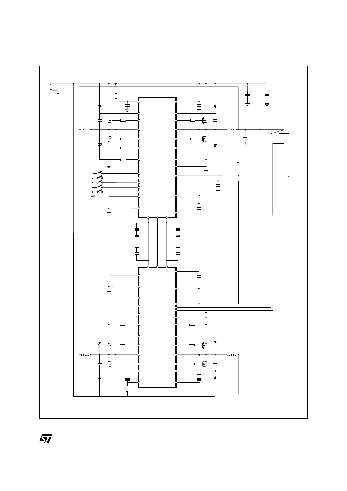
FOUR PHASE REFERENCE SCHEMATICS
g
Vin
NDin
VCCDR
2
HS1
L1
LS1
S4
S3
S2
S1
S0
UGATE1
PHASE1
LGATE1
Rg
PGNDS1
Rg
OSC / INH
BOOT1
ISEN1
VID4
VID3
VID2
VID1
VID0
SGND
VPROG_OUT
5
4
3
1
13
14
L6918A
Master
22
21
20
19
18
17
7
10
L6918 L6918A
C
VCC
6
BOOT2
24
25
26
27
16
15
28
23
11
12
SYNC_OUT
SLAVE OK
9
8
UGATE2
PHASE2
LGATE2
ISEN2
PGNDS2
PGND
PGOOD
FB
COMP
HS2
LS2
L2
Rg
Rg
R
FB
R
F
C
F
IN
C
OUT
CPU
PGOOD
SYNC_IN
VPROG_IN
SGND
ISEN1
22 21 20
17
7
23
18
19
14
L6918
13
1
3
4
5
2
Slave
OSC / INH
R2
To Slave’s
PGOOD
PGOOD
SYNC_OUT
SYNC/ADJ
Rg
PGNDS1
R
LS3
LGATE1
L3
HS3
PHASE1
UGATE1
BOOT1
VCCDR
SLAVE_OK
8
9
10
11
12
28
15
16
27
26
25
24
6
COMP
FB
VSEN
FBR
FBG
PGND
PGNDS2
ISEN2
LGATE2
PHASE2
UGATE2
BOOT2
VCC
C
F
R
F
R
F
Rg
Rg
LS4
HS4
L4
9/35

L6918 L6918A
V
R
R
DEVICES DESCRIPTION
The devices are integrated cir cui t realized i n BCD technology. They prov ide, in kit, a complete control logic and
protections sets for a high performance four-phases step-down DC-DC converter optimized for microprocessor s
supply and High Density DC-DC converters. They are designed to drive N-Channel mosfets in an interleaved
four-phase synchronous-rec tified buck topology. Each controller provi des a 180 deg phase shift betw een its two
phases and a 90deg phase-shifted syn chronizatio n signal is passed from the mas ter to the slave c ontroller that
locks the signal through a PLL. The resulting four-phases converter synchronized together results in a 90 deg
phase shift on each phase, al lowing a consistent reductio n of the input ca pacitors ripple cur rent, minimizing al so
the size and the power losses. The output voltage of the converter can be precisely regulated, programming the
master's VID pins, from 1.100V to 1.850V with 25mV binary steps. The reference for the regulation is passed
from the master device to the slave device through apposite pin likewise the synchronization signal. Each device
provides an average cur rent- mode control with fast tr ansient response. They inc lude a 300kHz free-running oscillator externally adjustable up to 600kHz, realized in order to multiply by 4 times the equivalent system frequency. The error amplifier features a 15MHz gain-bandwidth product and 10V/
converter bandwidth for fast transient performances. Current information is read in all the devices across the
lower mosfets R
or across a sense resistor in fully differential mode. The current information corrects the
DSON
PWM output in order to equalize the av erage current carried the two phases of each device. Cur rent sharing
between the two phases of each device is then limited at ±10% over static and dynamic conditions. Current
sharing between devices is assured by the droop function. The device protects against over-current, with an
OCP threshold for each phase, ent eri ng in constant cur rent mode. S ince the cur rent is read across the low s ide
mosfets, the constant current keeps c onstant the bot tom of the inductors current triangular waveform. When an
under voltage is detected the Slave device latches. The Slave device also perform an over voltage protection
that disable immediately both devices turning ON the lower driver and driving high the FAULT pin. Over Load
condition are transmitted from the Slave device(s) to the master through the SLAVE_OK line.
µ
s slew rate that permits high
MASTER - SLAVE INTERACTIONS
Figure 1. Four P has e connectio n wi th L6 918 family
ID 9.0
L6918A
L6918
Master and slave devices are connected together in order to realize four-phase high performance step-down
DC/DC converter. Four-phase c onver ter is implemented using L6918A master and one L6918 slave devices as
shown in figure 1.
A communication bus is implemented among all the controllers involved in the regulation. This bus consists in
the following lines:
Reference (VPROG_IN / VPROG_OUT pins):
–
The devices share the reference for the regulation. The reference is programmed through the master
device VID pins. It exits from the master through the VPROG_OUT pin and enters the slave device
through the VPROG_IN pin(s). Filter externally with at least 1nF capacitor.
MASTER CONTROLLE
SYNC_OUT
VPROG_OUT
SLAVE_OK
PGOOD PGOOD
OSC
Unidirectional line.
SYNC_IN
VPROG_IN
SLAVE_OK
OSC
SYNC_OUT
SLAVE CONTROLLE
10/35

L6918 L6918A
Clock Signal (SYNC_IN / SYNC_OUT pins):
–
A synchronization signal exits from the Master device through the SYNC_OUT pin with 90 deg phaseshift and enters the Slave device through the SYNC_IN pin. The Slave device locks that signal
through an internal PLL for its regulation. An auxiliary synchronizat ion signal exits from the Slave
through the SYNC_OUT.
SLAVE_OK Bus (SLAVE_OK pins):
–
Bi-directional line.
While the supply voltages are increasing, this line is hold to GND by all the devices. The Slave device
sets this line free (internally 5V pulled-up) when i t is ready for the Soft-Start. After that this line is
freed, the Master device starts the Soft Start (for further details about Soft-Start, see the relevant section).
During normal operation , the line is pulled low by the S lave d evice if an Over / Under v oltage i s detected (See relevant section).
– PGOOD pins:
PGOOD pins are connected together and pulled-up. During Soft-Start, the master device hold down
this line while during normal regulation the slave device de-assert the line if PGOOD has been lost.
Connections between the devices are shown in figure 1.
OSCILLATOR
The devices have been designed in order to operate on each phase at the same switching frequency of the internal oscillator. So, input and output resulting frequencies are four times bigger.
The oscillator is present in all the devices. Since the Master oscillator sets the main frequency for the regul ation,
the Slave oscillator gives an offset to the Slave's PLL. In this way the PLL is able to lock the synchronization
signal that enters from its SYNC_IN pin; it is able to recover up to ±15% offset in the sync hronization signal frequency. It is then necessary to program the switching frequency for all the devices involved in the multi-phase
conversion as follow.
The switching frequency is internally fixed to 300kHz. The internal oscillator generates the triangular waveform
for the PWM charging and discharging with a constant c urrent an internal capacit or. The current deliver ed to the
oscillator is typically 25
µ
A (Fsw = 300KHz) and may be varied using an external resistor (R
tween OSC pin and GND or Vcc. Since the OSC pin is maintained at fixed voltage (typ. 1.235V), the frequency
is varied proportional ly to the current sunk (forced) fr om (into) the pin consider ing the in ternal gain of 12K Hz/
In particular connecting it to GND the frequency is increased (current is sunk from the pin), while connecting
ROSC to Vcc=12V the frequency is reduced (current is forced into the pin), according to the following relationships:
Unidirectional line.
) connected be-
OSC
µ
A.
R
OSC
R
OSC
Note that forcing a 25
1.237
vs. GND:
vs. 12V:
µ
A current into this pin, the device stops switching because no current is delivered to the
fS300kHz
f
300kHz
S
----------------------------- 12
KΩ()
R
OSC
12 1.237–
----------------------------- 12
R
KΩ()
OSC
KHz
------------ 300KHz
µA
KHz
------------ 300KHz
µA
14.82 10
-----------------------------+=⋅+=
R
OSC
12.918 10
--------------------------------–=⋅+=
R
OSC
6
⋅
KΩ()
7
⋅
KΩ()
oscillator.
Figure 2 shows the frequency variation vs . the oscillator resistor ROSC considering the above repor ted relation-
ships.
11/35

L6918 L6918A
Figure 2. R
) vs. 12V
Ω
Rosc(K
vs. Switching Frequency
OSC
7000
6000
5000
4000
3000
2000
1000
0
0 100 200 300
Frequency (KHz)
1000
900
800
700
600
) vs. GND
500
Ω
400
300
200
Rosc(K
100
0
300 400 500 600
Frequency (KHz)
DIGITAL TO ANALOG CONVERTER (ONLY FOR MASTER DEVICE L6918A)
The built-in digital to analog converter allows the adjustment of the output voltage fr om 1.100V to 1.850V with
25mV as shown in the previous table 1. The internal reference is tr immed to ensure the precision of ±0.6% and
a zero temperature coefficient around the 70° C. The internal reference voltage for the regulation is programmed
by the voltage identification (VID) pins. These are TTL compatible inputs of an internal DAC that is realized by
means of a series of resistor s providing a parti tion of the inter nal voltage reference. The V ID code drives a multiplexer that selects a voltage on a precise point of the divider. The DAC output is delivered to an amplifier obtaining the VPROG voltage reference (i.e. the set-point of the error amplifier). Internal pull-ups are provided for
the VID pins (realized with a 5
µ
A current generator); in this way, to program a logic "1" it is enough to leave the
pin floating, while to program a logic "0" it is enough to short the pin to GND.
The voltage identification (VID) pin configuration also sets the power-good thresholds (PGOOD) and the Over/
Under voltage protection (OVP/UVP) thresholds.
The reference for the regulation is generated into the master device and deliv ered to the slave device through
the VPROG_OUT / VPROG_IN pins.
Programming the "11111" VID code, the device enters the NOCPU state: both devices keeps all mosfets OFF
and the condition is latched. Cycle the power supply to restart operation. Moreover, in this condition, the OVP
protection is still active into the slave device with a 0.8V threshold.
SOFT START AND INHIBIT
At start-up a ramp is generated from the master device increasing its loop reference from 0V to the final value
programmed by VID in 2048 clock periods. The same reference is present on the VPROG_OUT pin, producing
an increasing loop reference also into the slave device. In this way all the devices involv ed in the multi-phase
conversion start together with the same increasing reference (See Figure 3).
Before soft start, the l ower p ower MOS are turned ON after that VCCDR r eaches 2V (independentl y by V cc value) to discharge the output capacitor and to protect the load from high side mosfet failures. Once soft start begins, the reference is increased and also the upper MOS begins to switch: the output voltage starts to increase
with closed loop regulation. At the end of the digital soft start, the Power Good comparator is enabled and the
PGOOD signal is then driven high (See fig. 3). The Under Voltage compar ator is enabled when the reference
voltage reaches 0.8V.
The Soft-Start will not take place, if both VCC and VCCDR pins are not above their own turn-on thresholds. The
soft-start takes place, and the Master device starts to increase the reference, only if the SLAVE_OK bus is at
high level. The Slave device keeps this line shorted to GND until it is ready for the start-up while the master
keeps this line free before soft-start; anyway, this line is shorted to GND if VCC and VCCDR are not above the
turn-ON threshold. During normal operation, if any under-voltage is detected on one of the two supplies, the
devices are shutdown.
12/35

Figure 3. Soft Start
V
CC
L6918 L6918A
SLAVE_OK
VPROG_OUT
SYNC_OUT
PGOOD
LS
CH1=PGOOD; CH2=LGATEx; CH3=VPROG_OUT; CH4=SLAVE_OK
Forcing the master OSC/INH/FAULT pin to a voltage lower than 0.8V, the devices enter in IN HIBIT mode: all
the power mosfets are turned off until this condition is removed. When this pin is freed, the O SC/INH/FAULT
pin reaches the band-gap voltage and the soft start begin as previously explained.
In INHIBIT mode the Slave device still have both O VP and UVP protection ac tive refer ring the thr eshol ds to the
incoming reference present at the VPROG_IN pin if this one is greater than 0.8V. Otherwise (VPROG_IN <
0.8V) UVP is disabled and the OVP threshold is fixed at 0.8V.
DRIVER SECTION
The integrated high-current drivers allow using different types of power MOS (also multiple MOS to reduce the
RDSON), maintaining fast switching transition.
The drivers for the high-side mosfets use BOOT pins for supply and PHASE pins for return. The drivers for the
low-side mosfets use VCCDRV pin for supply and PGND pin for return. A minimum voltage of 5V at VCCDRV
pin is required to start operations of the device. The controller embodies a sophi sticated anti-shoot- through system to minimize low side body diode conduc tion time so mai ntaining good effi ciency saving the us e of Schottky
diodes. The conduction time is reduced to few nanoseconds assuring that high-side and low-side mosfets are
never switched on simultaneously: when the high-side mosfet turns off, the voltage on its source begins to fall;
when the voltage r eaches 2V, the low-side mos fet gate dri ve is applied w ith 30ns del ay. When the low- side mosfet turns off, the voltage at LGATE pin is sensed. When it drops below 1V, the high-side mosfet gate drive is
applied with a delay of 30ns. If the cur rent flowing in the inductor is negative, the source of high-side mosf et will
never drop. To allow the turning on of the low-side mosfet even in this case, a watchdog controller is enabled:
if the source of the high-side mosfet don't drop for more than 240ns, the low side mosfet is switched on so allowing the negative current of the inductor to recirculate. This mechanism allows the system to regulate even if
the current is negative.
The BOOT and VCCDRV pins are separated from IC's power supply (VCC pin) as well as signal ground (SGND
pin) and power ground (PGND pin) in order to maximize the switching noise immunity.
The peak current is shown for both the upper and the lower driver of the two phases in figure 4.A 10nF capacitive
load has been used.
For the upper drivers, the source current is 1.9A while the sink current is 1.5A with V
BOOT-VPHASE
ilarly, for the lower drivers, the source current is 2.4A while the sink current is 2A with V
CCDR
= 12V; sim-
= 12V.
13/35

L6918 L6918A
Figure 4. Drivers peak current: High Side (left) and Low Side (right)
CH3 = HGATE1; CH4 = HGATE2 CH3 = LGATE1; CH4 = LGATE2
CURRENT READING AND OVER CURRENT
Each device inv olved in the four phase convers ion has its own curr ent readin g cir c uitry and over c urrent protection. As a results, the OCP network design for each device must be performed fort half of the maximum output
current.
The current flowing trough each phase is read using the voltage drop across the low side mosfets R
across a sense resistor (R
) and internally converted into a current. The transconductance ratio is issued
SENSE
by the external resistor Rg placed outsi de the chip between ISENx and PGNDSx pins toward the reading points.
The full differential current readi ng rejects noi se and allow s to plac e sensing el ement in different lo cations w ithout affecting the measurement's accuracy. The current reading circuitry reads the current during the time in
which the low-side mosfet is on (OFF Time). During this time, the reaction keeps the pin ISENx and PGNDSx
at the same voltage while during the time in which th e reading circ uitry is off, an internal clamp keeps these two
pins at the same voltage sinking from the ISENx pin the necessary current (Needed if low-side mosfet R
sense is implemented to avoid absolute maximum rating overcome on ISENx pin).
The proprietary current reading circuit allows a very precise and high bandwidth reading for both positive and
negative current. This circuit reproduces the current flowing through the sensing element using a high speed
Track & Hold Tran conductance amplifier. In particular, it reads the current during the second half of the OFF
time reducing noise injection into the device due to the high side mosfet turn-on (See fig. 5). Tr ack time must
be at least 200ns to make proper reading of the delivered current.
This circuit sources a constant 50
µ
A current from the PGNDSx pin and keeps the pins ISENx and PGNDSx at
the same voltage. Referring to figure 5, the current that flows in the ISENx pin is then given by the following
equation:
DSON
or
dsON
R
---------------------------------------------
Where R
I
ISENx
is an external sense resis tor or the R
SENSE
50µ A
resistor used between ISE Nx and PGNDSx pins toward the readi ng points; I
⋅
SENSEIPHASE
R
g
of the low side mosfet and Rg is the tr ansconductance
dsON
50µ AI
+=+=
INFOx
is the current car ried by each
PHASE
phase.
The current information reproduced internally is represented by the second term of the previous equation as
follow:
14/35

L6918 L6918A
A
I
INFOx
R
---------------------------------------------=
⋅
SENSEIPHASE
R
g
Since the current is read in differential mode, also negative current information is kept; this allow the device to
check for dangerous returning current between the two phases assuring the complete equalization between the
phase's currents.
Figure 5. Current reading timing (left) and circuit (right)
I
LS1
LGATEX
I
LS2
Total
current
information
Track & Hold
ISENX
PGNDSX
From the current information for each phase, information about the total current delivered ( IFB=II
and the average current for each phase ( I
AVG
=(I
INFO1+IINFO2
)/2 ) is taken. I
INFOX
Rg
R
SENSE
NFO1+IINFO2
PHASE
I
50
I
ISENx
Rg
µµ
is then compared to I
AVG
to
give the correction to the PWM output in order to equalize the current carried by the two phases.
The transconductance resistor Rg can be designed in order to have current information of 25
full nominal load; the over current intervention threshold is set at 140% of the nominal (II
ing to the above relationship, the over current threshold (I
) for each phase, which has to be placed at one
OCPx
µ
A per phase at
= 35µA). Accord-
NFOx
half of the total delivered maximum current, results:
)
35µAR
⋅
I
OCPx
--------------------------=
R
g
SENSE
An over current is detected when the cur rent flowi ng into the sens e element is greater than IOCP (I
R
g
I
⋅
OCPxRSENSE
----------------------------------------- -=
35µA
INFO x
>35µA):
the device enters in Quasi-Constant-Current operation. The low-side mosfets stays ON until IINFO becomes
lower than 35
µ
A skipping clock cycles. The high side mosfets can be turned ON with a TON imposed by the
control loop at the next available clock cycle and the device works in the usual way until another OCP event is
detected.
The device limits the bottom of the inductor current triangular waveform. So the average current delivered can
slightly increase also in Over Current conditi on since the current ripple increases. In fact, the ON time increases
due to the OFF time rise because of the current has to reach the I
bottom. The worst-c ase conditio n is when
OCP
the duty cycle reaches its maximum value (d=50% internally limited). When this happens, the device works in
Constant Current and the output voltage decr ease as the load i ncrease. Crossing the UVP threshold causes the
Slave device to pul l down the SLAVE_OK l ine. All mosfets ar e turned off and all the dev ices involved in the regulation stop working. Cycle the power supply to restart operation.
Figure 6 shows the constant current working condition
15/35

L6918 L6918A
Figure 6. Con s ta nt C urrent opera ti on
TonMAX
Ipeak
I
MAX
I
OCPx
TonMAX
Vout
UVP
(IFB=50µA)
Droop effect
2·I
(IFB=70µA
OCPx
Iout
I
MAX,TO
It can be observed that the peak current (Ipeak) is greater than the 140% but it can be determined as follow:
Where Vout
VINVout
–
Ipeak I
is the minimum output voltage (UVP threshold).
MIN
OCPx
-------------------------------------
+=
min
Ton
L
⋅
MAXIOCPx
VINVout
–
--------------------------------------
+=
L
MIN
0.5 T⋅⋅
The device works in Constant-Current, and the output voltage decreases as the load increase, until the output
voltage reaches the under -voltage threshold (Vout
). When this threshold is crossed, all mosfets are turned
MIN
off, the FAULT pin is driven high and the device stops working. Cycle the power supply to restart operation. The
maximum average current during the Constant-Current behavior results:
Ipeak I
–
I
MAX TOT
2I
⋅
=
,
=
MAX
2I
⋅
OCPx
------------------------------------- -+
OCPx
2
In this particular situation, the switching frequency results reduced.
The ON time is the maximum allowed (T
T
Over current is set anyway when I
venient values for I
. Since the OCP intervention threshold is fixed, to modify the percentage w ith respect to
FB
OFF
=
INFO x
L
reaches 35µA. The full load value is only a convention to w ork w ith con-
) while the OFF time depends on the application:
onMAX
Ipeak I
–
V
OCPx
OUT
------------------------------------- -
⋅
f
1
------------------------------------------=
Ton
+
MAXTOFF
the load value, it can be simply considered that, for example, to have on OCP threshold of 170%, this will correspond to I
= 35µA (IFB = 70µA). The full lo ad current will then correspond to I
INFOx
= 20.5µA (IFB = 41µA).
INFO x
INTEGRATED DROOP FUNCTION
The devices use the droop function to satisfy the requirements of high performance microprocessors, reducing
the size and the cost of the output capacitor.
This method "recovers" part of the drop due to the output capacitor ESR in the load transient, introducing a dependence of the output voltage on the load current
As shown in figure 7, the ESR drop is pr esent in any c ase, but using the droop func tion the total deviation of the
output voltage is minimized. In practice the droop function introduces a static error proportional to the output
current that can be r epresented by a n equivalent output resistance R
. Since the device has an av erage cur-
OUT
rent mode regulation, the information about the total current delivered is used to implement the Droop Function.
This current (equ al to the sum of both I
) is sourced from the FB pin. Connecting a resistor between this pin
INFO x
and Vout, the total current information flows only in this resistor because the compensation network between
16/35

L6918 L6918A
(a) (b)
P
FB and COMP has always a capacitor i n series (See fig. 8). The volt age regulated b y each device is then equal
to:
R
SENSE
V
OUT
VID RFBI
FB
VID R
FB
--------------------- -
⋅⋅–=⋅–=
Rg
I
OUT
Where I
is the output current of each device (equal to the total load current I
OUT
divided by the number of
LOAD
devices N)
Since I
depends on the current infor mati on about the two phases of each device, the output characteristic vs.
FB
load current is given by:
R
FB
SENSE
--------------------- - I
Rg
Where R
OUT
VID RFBI
V
is the equivalent output resistance due to the droop function and I
OUT
OUT
VID R
each device (that is the total current delivered to the load I
OUT
divided by 2.
LOAD
VID R
R
SENSE
--------------------- -
FB
Rg
is still the output current of
OUT
Figure 7. Output transient response without (a) and with (b) the droop function
ESR DRO P ESR DROP
MAX
V
NOM
V
MIN
V
I
LOAD
---------------⋅⋅–=⋅⋅–=⋅–=
2
DROO
V
Figure 8. Active Droop Function Circuit
DROOP
DROOP
V
V
R
R
FB
FB
COMP FB
COMP FB
Total Current Info (I
Total Current Info (I
Ref
Ref
The feedback current is equal to 50µA at nominal full load (IFB = I
INFO 1
tion threshold, so the maximum output voltage deviation is equal to:
FULL_POSITIVE_LOAD
+RFB50µA⋅=
∆V
OL_INTERVENTION
INFO1+IINFO2
INFO1+IINFO2
+ I
INFO 2
OUT
OUT
To V
To V
)
)
) and 70µA at the OCP interven-
+RFB70µA⋅=∆V
17/35

L6918 L6918A
Droop function is provided only for positive load; if negative load is applied, and then IINFOx<0, no current is
sunk from the FB pin. The device regulates at the voltage programmed by the VID.
OUTPUT VOLTAGE MONITORING AND PROTECTION: POWER GOOD
The output voltage is monitored by the Slave devic e through the pin VS EN. If it is not within +12/-10% (typ.) of
the pro gramme d v alue, the P GOOD ou tput is for c ed low. PGOO D is a lway s acti ve in the Slav e devic e, also du ring soft-start. PGOOD in the Master device has the only masking function during soft-start. Since the master
has not the output voltage sense, it keeps the PGOOD to GND during soft-start and after this step it is freed.
The Slave device provides Over-Voltage protection: when the voltage sensed by VSEN reaches 117% (typ.) of
the reference voltage present at the VPROG_IN pin, the Slave device stops switching keeping the LS mosfets
ON. The FAULT pin is driven high (5V) and the SLAVE_OK line is pulled low. The master device then stops
switching keeping the LS mosfets ON, too. Since the condition is latched, power supply (Vcc) turn off and on is
required to restart operations.
Under voltage protection is also provided and still detected by the Slave device. If the output voltage drops below the 60% (typ.) of the reference voltage present at the VPROG_IN pin for more than one clock period, the
Slave device stops switching turning OFF all mosfets and pulling down the SLAVE_OK line: the Master device
stops switching with LS mosfets ON. The OSC/INH/FAULT is not driven high in this case.
Both Over Voltage and U nder Voltage are active also during soft start (Under V oltage after than Vout reaches
0.8V). During soft-start the refer ence volta ge used to determine the U V thresho ld is the incr easing vol tage driven by the 2048 soft start digital counter. Moreover, OVP is always active, even during INHIBIT (see relevant
section).
Over / Under Voltage behavior are shown in Figure 9.
Figure 9. OVP and UVP latch
SLAVE_OK
OSC
LS
UND ER VOLTAGE LATCH
L6918A
L6918
SLAVE_OK
OSC
LS
OVER VOLTAGE LATCH
L6918
L6918A
REMOTE VOLTAGE SENSE
A remote sense buffer is integrated into the dev ice to allow output voltage remo te sense implementation without
any additional external components. In this way, the output voltage programmed is regulated between the remote buffer inputs compensating motherboard trace losses or connector losses if the device is used for a VRM
module.
The very low offset amplifier senses the output vol tage remotely thr ough the pins FBR and FBG (FBR is for the
regulated voltage sense while FBG is for the ground sense ) and reports th is voltage internally at VSEN pin with
unity gain eliminating the err ors. Keeping the FBR and FBG traces parallel and guarded by a power plane results in common mode coupling for any picked-up noise.
If remote sense i s not requir ed, the output v oltage is s ensed by the VSEN pin c onnecting it di rectly to the output
voltage. In this case the FBG and FBR pins must be connected anyway to the regulated voltage
18/35

L6918 L6918A
INPUT CAPACITOR
The input capacitor is designed considering mainly the input rms current that depends on the duty cycle as reported in figure. Considering the four phase topology, the input rms current is highly reduced comparing with
single or dual phase operation.
It can be observed that the input rms value is one half of the dual-phase equivalent input current in the worstcase condition that happens for D=1/8, 3/8,5/8 and 7/8.
The power dissipated by the input capacitance is then equal to:
P
RMS
ESR I
2
()
⋅=
RMS
Input capacitor is designed in order to sustain the ripple relative to the maximum load duty cycle. To reach the
high rms value needed by the CPU power supply application and also to minimize components cost, the input
capacitance is realized by more than one physical capacitor. The equivalent rms current is simply the sum of
the single capacitor's rms current.
Figure 10. Input rms Current vs. Duty Cycle.
)
OUT
/I
0.50
RMS
0.25
Rms Current Normalized (I
0.25
Duty Cycle (V
Single Phase
Dual Phase
0.50
OUT
4 Phase
0.75
/V
)
IN
OUTPUT CAPACITOR
Since the microprocessors require a current variation beyond 100A doing load transients, with a slope in the
range of tenth A/
µ
s, the output capacitor is a basic component for the fast response of the power supply.
Dual phase topology reduces the amount of output capacitance needed because of faster load transient response (switching frequency is doubled at the load connections). Current ripple cancellation due to the 180°
phase shift between the two phases also reduces requirements on the output ESR to sustai n a specified v oltage
ripple.
When a load transient is applied to the converter's output, for first few microseconds the current to the load is
supplied by the output capacitors. The controller recognizes immediately the load transient and increases the
duty cycle, but the current slope is limited by the inductor value.
The output voltage has a first drop due to the current variation inside the capacitor (neglecting the effect of the
ESL):
∆V
OUT
∆I
OUT
ESR⋅=
19/35

L6918 L6918A
µ
µ
A minimum capacitor value is required to sustain the current during the load transient without discharge it. The
voltage drop due to the output capacitor discharge is given by the following equation:
2
∆V
OUT
------------------------------------------------------------------------------------------ -=
2C
OUTVINminDMAXVOUT
∆i
OUT
L⋅
–⋅()⋅⋅
Where D
is the maximum duty cycle value. The lower is the ESR, the lower is the output drop during load
MAX
transient and the lower is the output voltage static ripple.
INDUCTOR DESIGN
The inductance value is defined by a compromise between the transient response time, the efficiency, the cost
and the size. The inductor has to be calculated to sustain the output and the input voltage variation to maintain
the ripple current
∆
IL between 20% and 30% of the maximum output current. The inductance value can be cal-
culated with this relationship:
V
OUT
--------------⋅=
⋅
V
IN
is the output voltage.
OUT
Where f
V
–
INVOUT
L
------------------------------
f
SW∆IL
is the switching frequency, VIN is the input voltage and V
SW
Increasing the value of the inductance reduces the ripple current but, at the same time, reduces the converter
response time to a load transient. The response time is the time required by the inductor to change its current
from initial to final value. Since the inductor has not finished its charging time, the output current is supplied by
the output capacitors. Minimizing the response time can minimize the output capacitance required.
The response time to a load transient is different for the application or the removal of the load: if during the application of the loa d the inductor is c harged by a voltage equal to the difference between the input and the output
voltage, during the removal it is discharged only by the output voltage. The following expressions give approximate response time for DI load transient in case of enough fast compensation network response:
t
application
L ∆I⋅
------------------------------= t
VINV
–
OUT
removal
L ∆I⋅
--------------=
V
OUT
The worst condition depends on the input voltage available and the output voltage selected. Anyway the worst
case is the response ti me after r emoval o f the load with the minimum output voltage programmed and the maximum input voltage available.
Figure 11. Inductor ripple current vs. Vout
20/35
9
8
7
6
5
4
3
2
Inductor Ripple [A]
1
0
0.5 1.5 2.5 3.5
Output V olt age [V ]
Figure 12 – Inductor ripple current vs. Vout
L=1. 5
H, Vin=12V
L=3
H, Vin=5V
L=2µH,
Vin=12V
L=3µH,
Vin=12V
L=1. 5µH,
Vin=5V
L=2µH,
Vin=5V

L6918 L6918A
MAIN CONTROL LOOP
The four phases c ontrol loo p is composed by two dual phases devic es that ar e i ndependent eac h other. So, the
compensation network and the control loop stability of each device don't depend on the other except for the fact
that the other converter represents a load for this one.
The L6918/A control loop is com posed by the Current S haring c ontrol loop and the Average Current Mode control loop. Each loop gives, with a proper gain, the correction to the PWM in order to minimize the error in its
regulation: the Current Sharing control loop equalize the currents in the inductors while the Average Current
Mode control loop fixes the output voltage equal to the reference programmed by VID. Figure 12 reports the
block diagram of the main control loop
Figure 12. Main Control Loop Diagram
L
+
+
D02IN1392
4/5
PWM1
1/5
1/5
PWM2
ERROR
AMPLIFIER
CURRENT
SHARING
DUTY CYCLE
CORRECTION
+
-
Z
F(S)
REFERENCE
PROGRAMMED
BY VID
FBCOMP
1
I
INFO2
I
INFO1
L
2
C
O
R
FB
R
O
CURRENT SHARING (CS) CONTROL LOOP
The devices are configured to work in a four sync hronized phase applicati on. Since the application is com posed
by two-phase devices that share reference and synchronization signal s, the current sharing between the phases
is realized in two different steps:
1. Sharing between the phases of the same device;
2. Sharing between devices.
The Current Sharing between phases of the same device uses the internal current information to correct the
PWM signal in order to equalize the current. Active current sharing is implemented using the information from
Tran conductance differential amplifier in an average current mode control scheme. A current reference equal
to the average of the read cur rent ( I
) is internally bui lt; the err or between the r ead c urrent and this refer ence
AVG
is converted to a voltage with a proper gain and it is used to adjust the duty cycle whose dominant value is set
by the error amplifier at COMP pin (See fig. 13).
The current sharing control is a high bandwidth control allowing current sharing even during load transients.
The current sharing error is affected by the choice of external components; choose precise Rg resistor (±1% is
necessary) to sense the current. The current sharing error is internally dominated by the voltage mismatch of
Tran conductance differential amplifier between phases; considering a voltage mismatch equal to 2mV across
the sense resistor, the current reading error is given by the follow ing equation:
Where
∆
I
is the difference between one phase current and the ideal current (I
READ
For Rsense=4m
∆I
READ
------------------- -
I
MAX
Ω
and Imax=40A the current sharing error is equal to 2.5%, neglecting errors due to Rg and
2mV
---------------------------------------=
R
⋅
SENSEIMAX
MAX/2
).
Rsense mismatches.
21/35

L6918 L6918A
Figure 13. Current Shari ng Control Loop.
+
PWM1
1/5
1/5
CURRENT
SHARING
DUTY CYCLE
CORRECTION
I
INFO2
I
INFO1
L
1
+
COMP
PWM2
D02IN1393
L
2
V
OUT
The current sharing between devices uses the droop function. Each device can be modeled with its Thevenin
equivalent circuit (that is an id eal vol tage source equal to the programmed voltage by V IDs and its r elated output
resistance R
output resistance R
), while the whole converter is modeled by the same ideal voltage source and an equivalent
OUT
DROOP=ROUT
/2;
Considering this modelization reported in figure 14, it can be seen that the rec irculating cur rent between devices
depends on the accuracy of the regulation.
The accuracy of the voltage source is given by the offset of the master error amplifier Vos (6mV typ) and depends on the ratio between this offset and the output voltage variation with load (R
OUT,IOUT
). The mismatch
between the regulated voltages causes a c onverter to sour ce a curr ent that is s unk by the other one. The accuracy related to droop resistance depends on precision of feedback current of the device I
R
, Transconductance resistors Rg and feedback resistors RFB.
SENSE
, sense resistors
FB
The current sharing error (CSE) results:
2
CSE
∆I
OUT
----------------
I
OUT
1
Vos
--------------------------------
-- -
2
R
⋅
OUTIOUT
∆ I
2
1
FB
-- -
------------
++ + +≡=
2
I
FB
1
-- -
2
Considering the external resistors tolerance of 1%, the typical current feedback accuracy of 2.5
4 phases operation, Error Amplifier offset Vos=6mV, droop resistance R
I
LOAD
=60A (I
OUT=ILOAD
CSE
/2), it results:
2
1
1
0.006V
----------------------------------
-- -
2
1.5mΩ 60A⋅
2.5µA
-- -
----------------
+ +++ 0.062 6.2%()==
2
50µA
2
1
-- -
2
2
0.01()
∆ R
FB
-------------- -
R
FB
2
-- -
0.01()
2
2
∆ R
2
SENSE
-- -
------------------------- -
2
R
SENSE
=1.5mΩ (R
DROOP
4
2
-- -
0.01()
2
2
2
∆ R
4
-- -
---------- -
2
OUT
2
g
R
g
µ
A/50µA (5%),
=2,R
DROOP
) and
Figure 14. Equivalent Circuit for current sharing error calculation
LOAD
22/35
Recirculating Current
V
PROG
R
OUT
R
I
OUT
OUT
L6918
I
OUT
L6918A
I
LOAD
V
OUT
R
VID
R
DROOP
I
LOAD
V
R
OUT
LOAD

L6918 L6918A
AVERAGE CURRENT MODE (ACM) CONTROL LOOP
The average current mode control loop is reported in figure 15. The current information IFB sourced by the FB
pin flows into R
The ACM control loop gain results (obtained opening the loop after the COMP pin):
implementing the dependence of the output voltage from the read current.
FB
G
LOOP
s()
PWM Z
--------------------------------------------------------------------------------------------------------------------–=
Z
s() ZLs()+()
P
s() R
F
DROOPZP
Z
s()
F
-------------- - 1
As()
s()+()⋅⋅
1
----------- -+
R
⋅+⋅
As()
FB
where:
Rsense
R
– is the equivalent output resistance determined by the droop function;
DROO P
–Z
(s) is the impedance resulting by the parallel of the output capacitor (and its ESR) and the applied
P
----------------------
Rg
R
⋅=
FB
load Ro;
–Z
(s) is the compensation network impedance;
F
(s) is the parallel of the two inductor impedance;
–Z
L
– A(s) is the error amplifier gain;
V
4
IN
------------------ -
PWM
– is the ACM PWM transfer function where ∆V
-- -
⋅=
5
∆V
OSC
is the oscillator ramp amplitude
osc
and has a typical value of 2V
Removing the dependence from the Error Amplifier gain, so assuming this gain high enough, the control loop
gain results:
G
LOOP
s()
4
-- -
5
V
------------------ -
⋅⋅ ⋅–=
∆V
IN
OSC
Z
s()
F
------------------------------------
Z
s() ZLs()+
P
Z
-------------- -+
P
R
s()
FB
Rs
------- -
Rg
With further simplifications, it results:
V
Z
Ro R
s()
G
LOOP
s()
4
-- -
5
IN
------------------ -
∆V
OSC
F
-------------- -
R
FB
+
DROOP
-------------------------------------
Ro
R
L
------ -+
2
----------------------------------------------------------------------------------------------------------------------------------⋅⋅⋅–=
s
Considering now that in the application of interest it can be assumed that Ro>>R
R
<<Ro, it results:
DROOP
G
LOOP
s()
4
-- -
5
⋅⋅⋅–=
V
IN
------------------ -
∆V
OSC
Z
s()
F
-------------- -
----------------------------------------------------------------------------------------------------------------------------------
R
FB
2
s
Co
1sCoR
L
2
Co
-- - s
2
1sCoR
L
-- - s
2
L
--------------- Co ESR Co
2Ro⋅
//Ro E S R+()⋅⋅+
DROOP
L
--------------- Co ESR Co
2Ro⋅
DROOP
ESR+()⋅⋅+
R
L
------ -⋅+⋅+ 1+⋅+⋅⋅
2
R
L
------ -
⋅+⋅+ 1+⋅+⋅⋅
2
; ESR<<Ro and
L
The ACM control loop gai n is designed to obtain a high D C gain to m inimiz e static er ror and cr os s the 0dB ax es
with a constant -20dB/dec slope with the desired crossover frequency
ω
T. Neglecting the effect of ZF(s), the
transfer function has one zero and two poles. Both the poles ar e fixed once the output filter is des igned and the
zero is fixed by ESR and the Droop resistance.
To obtain the desired shape an R
A zero at
ω
=1/RFCF is then introduced together with an integrator. This integrator minimizes the static error
f
series network is considered for the ZF(s) implementation.
F-CF
23/35

L6918 L6918A
while placing the zero in correspondence with the L-C resonance a simple -20dB/dec shape of the gain is assured (See Figure 15). In fact, considering the usual value for the output filter, the LC resonance results to be
at frequency lower than the above reported zero.
Figure 15. ACM Control Loop Gain Block Diagram (left) and Bode Diagram (right).
dB
I
FB
F
Z
C
V
COMP
PWM
d•V
Compensation network can be simply designed placing
desired obtaining:
R
F
F
R
FB
REF
L/2
IN
Cout
ESR
V
OUT
Rout
K
K
---------------
=
-- -
V
5
∆
ω
=
Z
V
4
1
IN
----------⋅⋅
R
osc
FB
ω
and imposing the cross-over frequency
LC
dB
G
LOOP
ZF(s)
ω
ω
Z
LC
ω
T
ω
ω
as
T
L
-- -
Co
⋅
2
--------------------=
R
F
R
F
R
⋅
FB∆VOSC
----------------------------------
V
IN
5
-------------------------------------------------------
---
⋅⋅ ⋅= C
ω
T
4
2R
L
DROOP
ESR+()⋅
F
In a four phase operation ( since the four phase converter is realized by tw o dual phase converters in parallel
that shares current using droop), also the other sub-system in parallel must be considered. In particular, in the
above reported relationships, it must be considered with Co and ESR the total output capacitance and equivalent ESR while the output impedance Zo of the other sub-system must be considered in parallel to the output
capacitance Co and to the load Ro.
The output impedance of the other sub-system in parallel results:
V
4
-- -
-------------------
5
∆V
4
-- -
1
5
Zo s()
ZLs()
-----------------------------------------------------------------------------------------------=
Considering Zo in parallel to Ro, it can be verified that the R
Rsense
IN
---------------------- Z
OSC
-------------------
⋅⋅+
∆V
Rg
V
Z
IN
F
-------------- -
R
OSC
FB
and CF design relationships are still valid.
F
s()
s()⋅⋅ ⋅+
F
LAYOUT GUIDE LINES
Since the device manages control functions and high -current driv ers, layout is one of the most imp ortan t things
to consider when designing such high current applications.
A good layout solution can generate a benefit in low ering power dissipation on the power paths, reducing radiation and a proper connection between signal and power ground can optimize the performance of the control
loops.
Integrated power drivers reduc e components count and interconnec tions between control fun ctions and drivers,
reducing the board space.
Here below are listed the main points to focus on when starting a new layout and r ules are suggested for a correct implementation.
24/35

L6918 L6918A
Power Connections.
These are the c onnections wher e switching and continuous current fl ows from the input supp ly towards the load.
The first priority when placing components has to be reserved to this power section, minimizing the length of
each connection as much as possible.
To minimize noise and vol tage spikes (EMI and l osses) these interconnections must be a part of a pow er plane
and anyway realized by wide and thick copper traces. The critical components, i.e. the power transistors, must
be located as close as possible, together and to the controller. Considering that the "electrical" components reported in figure ar e com posed by more than one "phy sical " component, a ground plane or "star" grounding connection is suggested to minimize effects due to multiple connections.
Fig. 16a shows the details of the power connections involved and the current loops. The input capacitance
(CIN), or at least a portion of the total capaci t ance needed, has to be pl aced clos e to the power sect ion in order
to eliminate the stray inductance generated by the copper traces. Low ESR and ESL capacitors are required.
Figure 16. Power connections and related connections layou t guidel ines (same for bo th phases).
HS
R
HGATEx
PHASEx
LGATEx
PGNDx
gate
L
C
LS
R
gate
D
C
IN
OUT
LOAD
a. PCB power and ground planes areas
VIN
SGND
BOOTx
PHASEx
VCC
C
BOOTx
HS
+VCC
LS
C
VCC
VIN
L
C
D
C
IN
OUT
LOAD
b. PCB small signal components placement
Power Connections Related.
Fig.16b s hows some smal l s ignal c omponen ts pl acement , and ho w an d where t o mix s ig nal a nd power g rou nd pl anes.
The distance from drivers and mosfet gates should be reduced as much as possible. Propagation delay times as
well as for the voltage spikes generated by the distributed inductance along the copper traces are so minimized.
In fact, the further the mosfet is from the device, the longer is the interconnecting gate trace and as a consequence,
the higher are the voltage spikes corresponding to the gate PWM rising and falling signals. Even if these spikes
are clamped by inherent internal diodes, propagation delays, noise and potential causes of instabilities are introduced j eop ar d izin g g o od sy st em be ha vi or. O ne im por tan t co nsequ en ce i s that t h e sw i tchi ng l os ses for the hi g h
side mosfet are significantly increased.
For this reason, it is suggested to have the device oriented with the driver side towards the mosfets and the GATEx
and PHA SEx tr ace s walki ng t oget her t owar d the high side m osfet in or der t o min imiz e dist anc e (se e fig 1 7). In
addit io n, s in ce t he PH ASE x pin is t he r etu r n pat h f or t h e hi gh side d r iv er, t hi s pi n m us t be co nn ec t ed di r ec t ly to
the High Side mo sfet Sourc e pin to have a pro per driv ing fo r this mos fet. Fo r the LS mo sfet s, the return path is the
PGND pin: it can be connected d irectly to the power ground plane (if implemented) or in the same way to the LS
mosfet s Sour ce pin . GATE x and P HASEx co nne ctio ns (and also P GND w hen no po wer gr oun d plan e is im plemented) must also be designed to handle current peaks in excess of 2A (30 mils wide is su ggested).
25/35

L6918 L6918A
Figure 17. Device orientation (left) and sense nets routing (right).
To LS mosfet
Towards HS mosfet
(30 mils wide)
Toward s LS mosfet
(30 mils wide)
(or sense resistor)
Towards HS mosfet
(30 mils wide)
To LS mosfet
(or sense resistor)
To regulated output
Gate resistors of few ohms help in reducing the power dissipated by the IC without compromising the system
efficiency.
The placement of other components is also important:
– The bootstrap capacitor must be placed as close as possible to the BOOTx and PHASEx pins to min-
imize the loop that is created.
– Decoupling capacitor from Vcc and SGND placed as close as possible to the involved pins.
– Decoupling capacitor from VCCDR and PGND placed as close as possible to those pins. This capac-
itor sustains the peak currents requested by the low-side mosfet drivers.
– Refer to SGND all the sensible components such as frequency set-up resistor (when present) and
also the optional resistor from FB to GND used to give the positive droop effect.
– Connect SGND to PGND on the load side (output capacitor) to avoid undesirable load regulation ef-
fect and to ensure the right precision to the regulation when the remote sense buffer is not used.
– An additional 100nF ceramic capacitor is suggested to place near HS mosfet drain. This helps in re-
ducing noise.
– PHASE pin spikes. Since the HS mosfet switches in hard mode, heavy voltage spikes can be ob-
served on the PHASE pins. If these voltage spikes overcome the max breakdown voltage of the pin,
the device can absorb energy and it can cause damages. The voltage spikes must be limited by prop-
er layout, the use of gate resistors, Schottky diodes in parallel to the low side mosfets and/or snubber
network on the low side mosfets, to a value lower than 26V, for 20nSec, at Fosc of 600kHz max.
Current Sense Connectio ns.
Remote Buffer:
–
The input connect ions for t his component mus t be rout ed as parallel nets from the
FBG/FBR pins to t he lo ad i n order to c omp ensat e losses a long the out put power traces and also t o
avoid the pick-up of any comm on m ode noise. Connecting these pin s in points fa r from the load wi ll
cause a non-optimum load regulation, increasing output tolerance.
Current Reading:
–
The Rg resistor has to be placed as close as possible to the ISENx and PGNDSx
pins in order to limit the noise injection into the device. The PCB traces connecting these resistors to
the reading point must be routed as parallel traces in order to avoid the pick-up of any common mode
noise. It's also important to avoid any offset in the measurement and to get a better precision, to connect the traces as close as possible to the sensing elements, dedicated current sense resistor or low
side mosfet R
– Moreover, when using the low side mosfet R
dsON
.
as current sense element, the ISENx pin is practi-
dsON
cally connected to the PHASEx pin. DO NOT CONNECT THE PINS TOGETHER AND THEN TO
THE HS SOURCE! The dev ice won't work properly because of the noise generated by the return of
the high side driver. In this case route two separate nets: connect the PHASEx pin to the HS Source
(route together with HGATEx) with a wide net (30 mils) an d the ISEN x pin to the LS Drai n (route together with PGNDSx). Moreover, the PGNDSx pin is always connected, through the Rg resistor, to
the PGND: DO NOT CONNECT DIRECTLY TO THE PGND! In this case the device won't work properly. Route anyway to the LS mosfet source (together with ISENx net).
Right and wrong connections are reported in Figure 18.
Symmetrical layout is also suggested to avoid any unbalance between the two phases of the converter
26/35

Figure 18. PCB layout connections for sense nets.
NOT CORRECT CORRECT
VIA to GND plane
To PHASE
connection
L6918 L6918A
To LS Drain
and Source
To HS Gate
and Source
Wrong (left) and correct (right) connections for the current reading sensing nets.
Interconnections between devices.
Master and Slave devices shar e reference and other signals for the r egulation. To avoid noise injection into devices, it is recommended to route these nets carefully.
VPROG_IN / VPRO G_O U T:
–
This is the reference for the regulation. It must be routed far away from
any noisy trace and guarded by ground traces in order to avoid noise injection into the device. It can
be filtered with a 30nF maximum of distributed capacitance vs. signal ground.
SLAVE_OK:
–
This signal is used by the devices for the start-up synchronization and also to communicate UVP from Slave to Master device. It must be filtered by 1nF capacitor near the pin of each device to avoid the noise to cause false protection's trigger.
Demo Board Description
The L6918 demo board shows the operation of the device in a four phases application. This evaluation board allows output voltage adjustability (1.100V - 1.850V) through the switches S0-S4 and high output current capability.
The board has been laid out with the possi bility to use up to two D
2
PACK mosfets for the low side sw itch in order
to give maximum flexibility in the mosfet choice.
µ
The four layers demo board's copper thickness is of 70
m in order to minimize conduction losses considering
the high current that the circuit is able to deliver.
Demo board schematic circuit is reported in Figure 19.
Several jumpers allow setting different configurations for the device: JP3, JP4 and JP5 allow configuring the
remote buffer as desired. Simply shorting JP4 and JP5 the remote buffer is enabled and it senses the output
voltage on-board; to implement a real remote sense, leave these jumpers open and connect the FBG and FBR
connectors on the demo board to the remote load. To avoid usi ng the remote buffer, simpl y short all the j umpers
JP3, JP4 and JP5. Local sense through the R7 is used for the regulation.
The input can be configured in different ways using the jumpers JP1, JP2 and JP6; these jumpers control also
the mosfet driver supply v oltage. Anyway, power c onversion starts fr om V
and the device is suppl ied from V
IN
CC
(See Figure 20).
27/35

L6918 L6918A
E
Figure 19. Demo Board Schematic
Vin
GNDin
GNDcc
Vcc
JP6
DZ1
JP1
C29
L3
To L6918A
Pin 6
C27
Q5a
D10
R37
JP2
R16
Q6
Q5
S4
S3
S2
S1
S0
R35
R38
R33
R27
R26
R23
C50
VCCDR
C31
BOOT1
UGATE1
PHASE1
LGATE1
PGNDS1
OSC / INH
ISEN1
SGND
VID4
VID3
VID2
VID1
VID0
VPROG_ OU T
2
5
4
3
1
13
14
L6918A
Master
22
21
20
19
18
17
7
11
10
R30
C12
C32
R34
R39
R32
R24
D9
Q8 C26
Q7
Q7a
C28
L4
R25
R22
C30
R29
C25
R28
C53
C48
R31
VCC
6
BOOT2
24
UGATE2
25
PHASE2
26
LGATE2
27
ISEN2
16
PGNDS2
15
PGND
28
PGOOD
23
FB
9
COMP
8
12
SYNC_OUT
SLAVE_OK
C9,C10;
C33,C34
C14..C23,
C35..C44
C24
R21
JP3
C11,C13,C5 1;
R19
R20
C46,C47,C5 2
VoutCOR
GNDCOR
PGOOD
JP5
JP4
To L6918
Pin 6
L1
C5
C4
Q1a
C49
VPROG_ IN
SYNC_IN
Slave
22 21 20
OSC / INH
D5
SGND
PGOOD
SYNC_OUT
SYNC/ADJ
PGNDS1
ISEN1
LGATE1
PHASE1
UGATE1
BOOT1
VCCDR
17
7
23
18
19
14
L6918
13
1
3
4
5
2
R36
R2
To Slave’s
PGOOD
SL/ADJ
R5
D4
R6
R13
Q1
R18
R15
Q2
C8
SLAVE_OK
8
9
10
11
12
28
15
16
27
26
25
24
6
C45
COMP
C2
R8
FB
C24
R11
VSEN
FBR
FBG
PGND
R4
PGNDS2
R3
ISEN2
D6
R12
LGATE2
PHASE2
UGATE2
BOOT2
VCC
R17
R14
C7
R10
C1
R7
Q3a
Q3
Q4 C3
D3
R9
L2
C6
FBR
FBG
28/35

Figure 20. Power supply co nfi guration
V
L6918 L6918A
Vin
JP6
GNDin
Vcc
GNDcc
Two main configur ations can be di stinguis hed: S ingle Supply ( VCC = VIN = 12V) and Double Supply (VCC = 12V
V
= 5V or different).
IN
– Single Supply: In this case JP6 has to be completely shorted. The device is supplied with the same rail
that is used for the conversion. With an additional zener diode DZ1 a lo wer voltage can be derived to
supply the mosfets driver if Logic level mosf et are us ed. In this c ase J P1 must be left op en so th at the
HS driver is supplied with V
the right to use V
and JP2 can be freely shorted in one of the two positions.
– Double Supply: In this cas e V
for the power conversion. This last one can start indifferently from the 5V bus (Typ.) or from other buses
allowing maximum flexibility in the power conversion. Supply for the mosfet driver can be programmed
through the jumpers JP1, JP2 and JP6 as previously illustrated. JP6 selects now V
on the requirements.
Some examples are reported in the following Figures 21 and 22.
IN-VDZ1
IN-VDZ1
to supply the LS driver through VCCDR pin. Otherwise, JP1 must be shorted
through BOOTx and JP2 must be shorted to the left to use VIN or to
supply directly the controller (12V ) while VIN supplies the HS drains
CC
DZ1
JP1
JP2
To Vcc pin
To HS Drains (Power Input)
To BOOTx (HS Driver Supply)
To VCCDR pin (LS Driver Supply)
or VIN depending
CC
Figure 21. Jumpers configuration: Double Supply
Vcc = 12V
Vcc = 12V
Vin = 5V
GNDin
GNDcc
Vin = 5V
GNDin
GNDcc
JP6
DZ1
JP1
(a) V
= 12V; V
CC
BOOTx
JP6
DZ1
JP1
(b) V
CC
= V
= VCCDR = 12V; VIN = 5V
BOOTx
Vcc = 12V
HS Drains = 5V
HS Suppl y = 5V
JP2
VCCDR (LS Supply) = 5V
= VCCDR = VIN = 5V
Vcc = 12V
HS Drains = 5V
HS Supply = 12V
JP2
VCCDR (LS Supply) = 12
29/35

L6918 L6918A
Figure 22. Jumpers configuration: Single Supply
Vcc = Open
Vcc = Open
PCB AND COMPONENT LAYOUT
Figure 23. PCB and Components Layouts (Dimensions: 10.8mm x 14.5mm)
Vin = 12V
GNDin
GNDcc
Vin = 12V
GNDin
GNDcc
JP6
DZ1 6.8V
JP1
JP2
(a) VCC = VIN = VCCDR = 12V; V
JP6
DZ1
JP1
JP2
(b) V
= VIN = V
CC
= VCCDR = 12V
BOOTx
Vcc = 12V
HS Drains = 12V
HS Supply = 5.2V
VCCDR (LS Supply) = 12V
BOOTx
Vcc = 12V
HS Drains = 12V
HS Supply = 12V
VCCDR (LS Supply) = 12V
= 5.2V
30/35
Component Side
Internal SGND Plane Solder Side
Internal PGND Plane

L6918 L6918A
CPU Power Supply: 12VIN; 1.45V
OUT
; 110A
DC
Considering the high slope for the load transient, a high switching frequency has to be used. In addition to fast
reaction, this helps in reducing output and input capacitor. Inductance value is also reduced.
A switching frequency of 200kHz for each phase is then considered allowing large bandwidth for the compensation network. Considering the high output current, power conversion will start from the 12V bus.
– Current Reading Network and Over Current:
Since the maximum output c urrent is I
= 110A, the over current threshold has be en set to 110A
MAX
(27.5A x 4) in the worst case (ma x mo sfet tempe rature). Since t he dev ice limi ts the val ley of t he t riangular ripple across the inductors, the current ripple must be considered too. Considering the inductor
core saturation, a current ripple of 10A has to be considered so that the OCP threshold in worst case
becomes OCPx = 22A (27.5A-5A). Considering to sense the output current across the low-side mosfets
RdsON (two in parallel to reduce equivalent R
), each STB90NF03L has 6.5mΩ max at 25°C that
dsON
becomes 9.1mΩ at 100°C considering the temperature variation; the resulting transconductance resistor Rg has to be:
R
dsON
----------------- -
OCPx
⋅
µ
35
===
Rg I
22
4.5m
-------------
⋅
35
2.7kΩ (R3 to R6; R24 to R27)
µ
– Droop function Design:
Considering a voltage drop of 85mV at full load, the feedback resistor R
85mV
----------------
==
R
FB
70µA
1.2kΩ (R7)
has to be:
FB
– Inductor design:
Transient response performance ne eds a comp romi se in the induct or ch oice value: t he bigg est the inductor, the highest the efficient but the worse the transie nt response and vice versa. Considering then
an inductor value of 1µH, the current ripple becomes:
–
Vin Vo ut
== =
∆
---------------------------- -
I
L
d
-----------⋅
Fsw
–
12 1.4
-------------------- -
µ
1
1.4
------- -
12
1
------------ -⋅⋅
200k
6.2A (L1, L2)
– Output Capacitor:
Ten Rubycon MBZ (3300µF / 6.3V / 12mΩ max ESR) has been used implementing a resulting ESR of
1.2mΩ resulting in an ESR voltage drop of 52A*1.2mΩ = 62mV after a 52A load transient.
– Compensation Network:
A voltage loop bandwidth of 20kHz is considered to let the device fast react after load transient.
The R
R
== =
F
network results:
F CF
R
∆⋅
IN
5
ω
⋅⋅ ⋅
-- -
T
4
FBVOS
------------------------------
V
-------------------------------------------------------
2R
L
()⋅
DROOP
== =
C
F
ESR
+
⋅
Co
------------------- -
R
F
1.2 K 2⋅
--------------------
L
-- -
63300
2
-----------------------------------------
12
3.9k
5
-- -
4
µ
⋅⋅
20 k 2Π
µ
1
------ -
2
⋅⋅⋅⋅ 3.9kΩ
----------------------------------------------------------
2
22nF
1 µ
4.5 m
⋅
-------------
2.7
1k 1.2m
⋅
+
(R8)
(C2)
Further adjustments can be done on the work bench to fit the requirements and to compensate layout parasitic
components.
31/35

L6918 L6918A
Part List
Resistors
R2, R9, R20, R23, R31, R42 Not Mounted SMD 0805
R3, R4, R5, R6
R24, R25, R26, R27
R7, R28 1.2K 1% SMD 0805
R11, R22 510 SMD 0805
R12 to R19
R32, R33, R34, R35, R38, R39
R8, R29 3.9K SMD 0805
R10, R30 82 SMD 0805
R21 10K SMD 0805
R36, R37 1M 1% SMD 0805
Capacitors
C1, C48 Not Mounted SMD 0805
C2, C25 47n SMD 0805
C24, C30 100n SMD 0805
C3, C4, C26, C27 100n SMD 0805
C5, C6, C7, C28, C29, C32 1µ SMD 0805
C8, C31 10µ SMD 1206
C9, C10, C33, C34 10µ or 22µ / 16V TDK Multilayer Ceramic SMD 1206
C11, C13, C46, C47,
C51, C52
C12, C45, C49, C50 1n SMD 0805
C53 1n SMD 0805
C14, C16, C18, C20, C22
C35, C37, C39, C41, C43
Diodes
D3, D4, D9, D10 1N4148 SOT23
DZ1 Not Mounted MINIMEL F
Mosfets
Q1, Q1A, Q3, Q3A,
Q5, Q5A, Q7, Q7A
Q2, Q4, Q6, Q8 STB90NF03L STMicroelectronics D2PACK
Inductors
L1, L2, L3, L4 1µ 77121 Core / 5 Turns 2 x 1.5 mm
Controllers
U2 L6918 STMicroelectronics SO28
2.7K 1% SMD 0805
0 SMD 0805
1800µ / 16V Rubycon MBZ Radial 23x10.5
3300µ /6.3V Rubycon MBZ Radial 23x10.5
STB90NF03L STMicroelectronics D2PACK
32/35

L6918 L6918A
STATIC PERFORMANCES
Figure 24 shows the demo board measured efficiency versus load current in steady state conditi ons without airflow at ambient temperature.
Figure 24. System Efficiency
90
85
80
75
70
Efficiency [%]
65
60
55
0102030405060708090100110
Figure 25 shows the mosfets temper ature versus output current in steady state condition without any air-flow
or heat sink. It can be observed that the mosfets are under 100°C in any conditions. Load regulation is also reported from 10A to 110A.
Output Cur r e nt [A]
Figure 25. Mosfet Temperature and Load Regulation.
110
100
90
C]
o
80
70
60
50
Temperature [
40
30
High-Side MOS
Low-Side MOS
0 102030405060708090100110
Output Current [A]
1.470
1.450
1.430
1.410
Vout [V]
1.390
1.370
1.350
0 102030405060708090100110
Output Current [A]
DYNAMIC PERFORMANCES
Figure 26 shows the system response to a load transient from 0A to 110A. The output voltage is contained in
the ±50mV range. Additional output capacitors can help in reducing the initial voltage spike mainly due to the
ESR.
Figure 26. 110A Load Transient Response.
33/35

L6918 L6918A
DIM.
MIN. TYP. MAX. MIN. TYP. MAX.
A 2.65 0.104
a1 0.1 0.3 0.004 0.012
b 0.35 0.49 0.014 0.019
b1 0.23 0.32 0.009 0.013
C 0.5 0.020
c1 45° (typ.)
D 17.7 18.1 0.697 0.713
E 10 10.65 0.394 0.419
e 1.27 0.050
e3 16.51 0.65
F 7.4 7.6 0.291 0.299
L 0.4 1.27 0.016 0.050
S8° (max.)
mm inch
OUTLINE AND
MECHANICAL DATA
SO28
34/35

L6918 L6918A
Information furnished is believed to be accurate and reliable. However, STMicroelectronics assumes no responsibility for the consequences
of use of such information nor for any infringement of patents or other rights of third parties which may result from its use. No license is granted
by implic ation or o th erwise un der any patent or patent ri ghts of STM i croelectronics. Specifications mentioned in this p ublication are subject
to change without notice. This publication supersedes and replaces all information previously supplied. STMicroelectronics products are not
authorized for use as c ri t i cal components in life support dev i ces or systems without express wri t ten approval of STMic roelectronics.
The ST logo is a registered trademark of STMicroelectronics
© 2002 STMic roelectroni cs - All Rights Reserved
Australia - Brazi l - Canada - Ch i na - F i nl and - Franc e - Germany - Hong Kong - India - Isr ael - Italy - Japan -Malay si a - Malta - Morocco -
Singap ore - Spain - Sweden - Swit zerland - U ni ted Kingdom - United S tates.
STMicroelectronics GROUP OF COMPANIES
http://www.s t. com
35/35
 Loading...