

Page 1
VERY PRECISE ADJUSTABLE OUTPUT
OVERVOLTAGEPROTECTION
MICROPOWERSTART-UPCURRENT (50µATYP.)
VERYLOW OPERATINGSUPPLY CURRENT
(4mA TYP.)
INTERNALSTART-UP TIMER
CURRENT SENSEFILTER ON CHIP
DISABLEFUNCTION
1% PRECISION (@ T
j
=25°C) INTERNAL
REFERENCEVOLTAGE
TRANSITIONMODE OPERATION
TOTEMPOLE OUTPUTCURRENT: ±400mA
DIP8/SO8PACKAGES
DESCRIPTION
L6561 is the improved version of the L6560
standard Power Factor Corrector. Fully compatible with the standard version, it has a superior
performant multiplier making the device capable
of working in wide input voltage range applications (from 85V to 265V) with an excellent THD.
Furthermore the start up current has been reduced at few tens of µA and a disable function
has been implemented on the ZCD pin, guaranteeing lower current consumption in stand by
mode.
Realisedin mixedBCD technology,the chip gives
the followingbenefits:
- micro powerstart up current
- 1% precisioninternal referencevoltage
(Tj= 25°C)
- Soft Output Over Voltage Protection
- noneedforexternallowpas sfilt eronthecurr e n t
sense
- verylowoperatingquiescentcurrentminimises
powerdissipation
The totem pole output stage is capable of driving
a Power MOS or IGBT with source and sink currents of +/- 400mA. The device is operating in
transition mode and it is optimised for Electronic
Lamp Ballast application, AC-DC adaptors and
SMPS.
April 1999
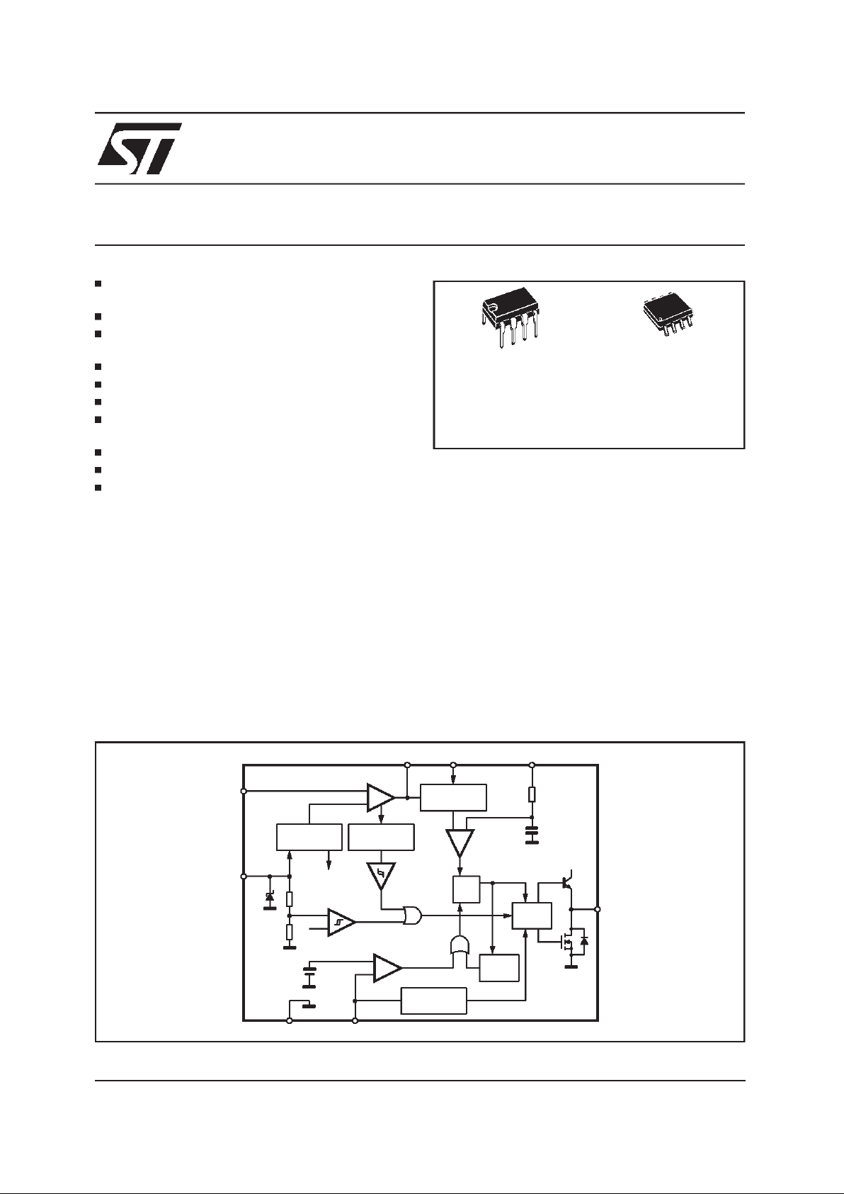
+
-
MULTIPLIER
V
REF2
OVER-VOLTAGE
DETECTION
VOLTAGE
REGULATOR
UVLO
INTERNAL
SUPPLY 7V
+
-
2.5V
R1
R2
RSQ
+-
DRIVER
STARTER
+
-
ZERO
CURRENT
DETECTOR
DISABLE
2.3V
1.8V
V
CC
8
1
23 4
ZCD
V
CC
INV
COMP MULT CS
GD
7
5
GND
6
D97IN547B
20V
40K
5pF
BLOCK DIAGRAM
Minidip SO8
ORDERING NUMBERS:
L6561 (Minidip)
L6561D
(SO8)
L6561
POWER FACTOR CORRECTOR
1/11
Page 2

THERMAL DATA
Symbol Parameter SO 8 MINIDIP Unit
R
th j-amb
ThermalResistance Junction-ambient
150 100 °C/W
PIN FUNCTIONS
N. Name Function
1 INV Inverting input ofthe error amplifier. A resistivedivider is connected betweenthe output
regulated voltage and this point, to provide voltage feedback.
2 COMP Output of error amplifier. A feedback compensation network is placed between thispin and
the INV pin.
3 MULT Input of themultiplier stage. A resistive dividerconnects to this pinthe rectified mains. A
voltage signal, proportional to the rectified mains, appears on this pin.
4 CS Input to thecomparator ofthe control loop. The current is sensedby a resistor and the
resulting voltage is applied to this pin.
5 ZCD Zero current detectioninput. If it is connected to GND, the device isdisabled.
6 GND Current return for driver and control circuits.
7 GD Gate driver output. A push pull output stage isable to drivethe Power MOS with peak current
of 400mA (source and sink).
8V
CC
Supply voltage of driver and control circuits.
PIN CONNECTION
ABSOLUTE MAXIMUM RATINGS
Symbol Pin Parameter Value Unit
I
V
cc
8ICC+I
Z
30 mA
I
GD
7 Output Totem Pole Peak Current (2µs) ±700 mA
INV, COMP
MULT
1, 2, 3 Analog Inputs & Outputs -0.3 to 7 V
CS 4 Current Sense Input -0.3 to 7 V
ZCD 5 Zero Current Detector 50 (source)
-10 (sink)
mA
mA
P
tot
Power Dissipation @T
amb
=50°C (Minidip)
(SO8)
1
0.65
W
T
j
Junction Temperature Operating Range -25 to 150
°
C
T
stg
Storage Temperature -55 to 150
°
C
L6561
2/11
Page 3
ELECTRICALCHARACTERISTICS(VCC= 14.5V; T
amb
= -25°C to 125°C;unless otherwisespecified)
SUPPLY VOLTAGE SECTION
Symbol Pin Parameter Test Condition Min. Typ. Max. Unit
V
CC
8 Operating Range after turn-on 11 18 V
V
CC ON
8 Turn-on Threshold 11 12 13 V
V
CC OFF 8 Turn-off Threshold 8.7 9.5 10.3 V
Hys 8 Hysteresis 2.2 2.5 2.8 V
SUPPLY CURRENT SECTION
Symbol Pin Parameter Test Condition Min. Typ. Max. Unit
I
START-U 8 Start-up Current before turn-on (V
CC
=11V) 20 50 90 µA
I
q 8 Quiescent Current 2.6 4 mA
I
CC Operating Supply Current C
L
= 1nF @ 70KHz 4 5.5 mA
in OVP condition V
pin1
= 2.7V 1.4 2.1 mA
I
q
Quiescent Current V
PIN5
≤
150mV, V
CC>VCC off
1.4 2.1 mA
V
PIN5
≤
150mV, V
CC<VCC off
20 50 90
µ
A
V
Z
8 Zener Voltage ICC= 25mA 18 20 22 V
ERROR AMPLIFIER SECTION
Symbol Pin Parameter Test Condition Min. Typ. Max. Unit
V
INV
1 Voltage Feedback Input
Threshold
T
amb
=25°C 2.465 2.5 2.535 V
12V< V
CC
<18V 2.44 2.56
Line Regulation V
CC
= 12 to18V 2 5 mV
I
INV
1 Input Bias Current -0.1 -1 µA
G
V
Voltage Gain Open loop 60 80 dB
GB Gain Bandwidth 1 MHz
I
COMP 2 Source Current V
COMP
= 4V, V
INV
= 2.4V -2 -4 -8 mA
Sink Current V
COMP
= 4V, V
INV
= 2.6V 2.5 4.5 mA
V
COMP
2 Upper Clamp Voltage I
SOURCE
= 0.5mA 5.8 V
Lower Clamp Voltage I
Sink
= 0.5mA 2.25 V
MULTIPLIERSECTION
Symbol Pin Parameter Test Condition Min. Typ. Max. Unit
V
MULT
3 Linear Operating Voltage 0to3 0 to3.5 V
∆V
CS
∆
V
mult
Output Max. Slope V
MULT
= from0V to 0.5V
V
COMP
= UpperClamp Voltage
1.65 1.9
K Gain V
MULT
=1V V
COMP
= 4V 0.45 0.6 0.75 1/V
CURRENT SENSECOMPARATOR
Symbol Pin Parameter Test Condition Min. Typ. Max. Unit
V
CS
4 Current Sense Reference
Clamp
V
MULT
= 2.5V
V
COMP
= Upper Clamp Voltage
1.6 1.7 1.8 V
I
CS 4 Input Bias Current V
OS
= 0 -0.05 -1 µA
t
d (H-L)
4 Delay to Output 200 450 ns
4 Current Sense Offset 0 15 mV
L6561
3/11
Page 4
OVER VOLTAGEPROTECTION OVP
The output voltage is expected to be kept by the
operation of the PFC circuit close to its nominal
value. This is set by the ratio of the two external
resistors R
1 and R2 (see fig. 2), taking into con-
sideration that the non inverting input of the error
amplifier isbiased inside the L6561at 2.5V.
In steady state conditions, the current throughR1
and R2 is:
I
R1sc
=
V
out
− 2.5
R1
= I
R2
=
2.5V
R2
and, if the external compensation network is
made only with a capacitor C
comp
, the current
throughC
comp equalszero.
When the output voltage increases abruptly the
current throughR1 becomes:
I
R1
=
V
outsc
+∆V
OUT
− 2.5
R1
=
I
R1sc
+∆
I
R1
Since the current through R2 does not change,
∆
I
R1
must flow through the capacitor C
comp
and
enter theerror amplifier.
Thiscurrentis monitoredinsidethe L6561andwhen
reachesabout37µA the outputvoltageof themulti-
plieris forcedto decrease,thusreducing theenergy
drawn from the mains . If the current exceeds 40µA,
the OVP protectionis triggered(Dynami cOVP),and
the externalpowertransistoris switched offuntilthe
currentfallsapproximatelybelow10µA.
However, if the overvoltage persists, an internal
comparator(Static OVP) confirms theOVP condition keeping the external power switch turned off
(see fig.1).
Finally, the overvoltage that triggers the OVP
functionis:
∆
Vout = R
1 ⋅
40µA.
Typical values for R
1,R2and C are shown in the
applicationcircuits. Theovervoltagecanbe setindependentlyfrom the average outputvoltage.The precision in setting the overvoltage threshold is 7% of
ELECTRICALCHARACTERISTICS
(continued)
ZERO CURRENT DETECTOR
Symbol Pin Parameter Test Condition Min. Typ. Max. Unit
V
ZCD
5 Input Threshold Voltage
Rising Edge
(1) 2.1 V
Hysteresis (1) 0.3 0.5 0.7 V
V
ZCD
5 Upper Clamp Voltage IZCD =20µA 4.5 5.1 5.9 V
V
ZCD
5 Upper Clamp Voltage I
ZCD
= 3mA 4.7 5.2 6.1 V
V
ZCD
5 Lower Clamp Voltage I
ZCD
= –3mA 0.3 0.65 1 V
I
ZCD
5 Sink Bias Current 1V≤V
ZCD
≤
4.5V 2
µ
A
I
ZCD
5 Source Current Capability -3 -10 mA
I
ZCD
5 Sink CurrentCapability 3 10 mA
V
DIS
5 Disable threshold 150 200 250 mV
I
ZCD
5 Restart Current After Disable V
ZCD
< Vdis; VCC>V
CCOFF
-100 -200 -300 µA
OUTPUT SECTION
V
GD
7 Dropout Voltage I
GDsource
= 200mA 1.2 2 V
I
GDsource
= 20mA 0.7 1 V
I
GDsink
= 200mA 1.5 V
I
GDsink = 20mA 0.3 V
t
r 7 Output VoltageRise Time CL = 1nF 40 100 ns
t
f 7 Output Voltage Fall Time CL = 1nF 40 100 ns
I
GD off
7IGDSink Current VCC=3.5V VGD= 1V 5 10 - mA
OUTPUT OVERVOLTAGE SECTION
I
OVP
2 OVP Triggering Current 35 40 45 µA
Static OVP Threshold 2.1 2.25 2.4 V
RESTART TIMER
t
START
Start Timer 70 150 400 µs
(1) Parameter guaranteed by design, not testedin production.
L6561
4/11
Page 5

the over v ol t age value (for ins tanc e ∆V = 60V ±
4.2V).
Disable function
The zero current detector (ZCD) pin can be used
for device disabling as well. By grounding the
ZCD voltage the device is disabled reducing the
supply current consumption at 1.4mA typical (@
14.5V supplyvoltage).
Releasing the ZCD pin the internal start-up timer
will restart the device.
+Vo
D97IN591
-
+
2
R1
R2
Ccomp.
E/A
1
2.5V
∆I
-
+
X PWM DRIVER
2.25V
40µA
∆I
Figure 2. OvervoltageProtection Circuit
V
OUT nominal
I
SC
40µA
E/A OUTPUT
2.25V
DYNAMIC OVP
STATIC OVP
D97IN592A
OVER VOLTAGE
10µA
Figure 1.
L6561
5/11
Page 6

8
3
BRIDGE
4 x 1N4007
R9 (*)
950K
C1
1µF
250V
R10
10K
C2
22µF
25V
FUSE 4A/250V
Vac
(85V to 135V)
R3 (*)
240K
D3 1N4150
D2
1N5248B
R2
100
10nF
C6
R1
T
5
6
L6561
7
21
C3 680nF
R5 MOS
STP7NA40
D1 BYT03-400
R7 (*)
950K
C5
100µF
315V
Vo=240V
Po=80W
+
-
D97IN549B
TRANSFORMER
T: core THOMSON-CSF B1ET2910A (ETD 29 x16 x10mm) OR EQUIVALENT (OREGA 473201A7)
primary 90T of Litzwire 10x 0.2mm
secondary 11T of#27 AWG (0.15mm)
gap 1.8mm for atotal primaryinductance of 0.7mH
R6 (*)
0.31
1W
R8
10K
1%
+
-
C7
10nF
NTC
4
(*) R3 = 2 x 120KΩ
R6 = 0.619Ω/2
R7 = 2 x 475KΩ, 1%
R9 = 2 x 475KΩ
10
68K
Figure3. TypicalApplication Circuit(80W, 110VAC)
8
3
BRIDGE
4 x 1N4007
R9 (*)
1.82M
C1
560nF
400V
R10
10K
C2
22µF
25V
FUSE 2A/250V
Vac
(175V to 265V)
R3 (*)
440K
D3 1N4150
D2
1N5248B
R2
100
10nF
C6
R1
T
5
6
L6561
7
21
C3 1µF
R5 MOS
STP5NA50
D1 BYT13-600
R7 (*)
998K
C5
56µF
450V
Vo=400V
Po=120W
+
-
D97IN550B
TRANSFORMER
T: core THOMSON-CSF B1ET2910A (ETD29 x16 x10mm) OR EQUIVALENT (OREGA 473201A8)
primary 90T of Litz wire 10 x 0.2mm
secondary 7T of #27AWG (0.15mm)
gap 1.25mm for a total primary inductance of 0.8mH
R6 (*)
0.41
1W
R8
6.34K
1%
+
-
C7
10nF
NTC
(*) R3 =2 x220KΩ
R6 = 0.82Ω/2
R7 = 2 x 499KΩ,1%
R9 = 2 x 909KΩ
4
68K
10
Figure 4. TypicalApplicationCircuit (120W, 220VAC)
8
3
BRIDGE
4 x 1N4007
R9 (*)
1.24M
C1
1µF
400V
R10
10K
C2
22µF
25V
FUSE 4A/250V
Vac
(85V to 265V)
R3 (*)
240K
D3 1N4150
D2
1N5248B
R2
100
12nF
C6
R1
T
5
6
L6561
7
21
C3 1µF
R5 MOS
STP8NA50
D1 BYT13-600
R7 (*)
998K
C5
47µF
450V
Vo=400V
Po=80W
+
-
D97IN553B
TRANSFORMER
T: core THOMSON-CSF B1ET2910A (ETD29 x 16 x 10mm) OR EQUIVALENT (OREGA 473201A8)
primary 90T of Litz wire 10x 0.2mm
secondary 7T of #27AWG (0.15mm)
gap 1.25mm for a total primary inductanceof 0.8mH
R6 (*)
0.41
1W
R8
6.34K
1%
+
-
C7
10nF
NTC
(*) R3= 2 x120KΩ
R6 = 0.82Ω/2
R7 = 2 x 499KΩ, 1%
R9 = 2 x 620KΩ
4
68K
10
Figure 5. Wide-RangeApplication (80W)
L6561
6/11
Page 7

-50 -25 0 25 50 75 100 125 T (°C)
38
39
40
41
I
OVP
(µA)
D94IN047A
Figure 7. OVPCurrent Thresholdvs.
Temperature
-25 0 25 50 75 100 125
T(°C)
9
10
11
12
13
V
CC-ON
(V)
V
CC-OFF
(V)
D94IN044A
Figure8. UndervoltageLockout Thresholdvs.
Temperature
Figure 6. P.C. Board and Components Layoutof the Figg. 3, 4 and 5 (1:1.25scale)
C
O
M
P
O
N
E
N
T
S
S
I
D
E
S
O
L
D
E
R
S
I
D
E
L6561
7/11
Page 8

-50 0 50 100
2.46
2.48
2.50
T(°C)
V
REF
(V)
D94IN048A
Figure 10. VoltageFeedback InputThreshold
vs. Temperature
D97IN548A
0 5 10 15 20 VCC(V)
0
0.005
0.01
0.05
0.1
0.5
1
5
10
ICC
(mA)
CL= 1nF
f = 70KHz
TA=25°C
Figure 9. SupplyCurrent vs. SupplyVoltage
0 100 200 300 400 IGD(mA)
0
0.5
1.0
1.5
2.0
V
PIN7
(V)
SINK
VCC= 14.5V
D94IN046
Figure 11. Output Saturation Voltagevs. Sink
Current
V
MULT
(pin3) (V)
D97IN555A
2.6
3.0
3.2
3.5
4.5
5.0
V
COMP
(pin2)
(V)
0 0.5 1.0 1.5 2.0 2.5 3.0 3.5 4.0 4.5
0
0.2
0.4
0.6
0.8
1.0
1.2
1.4
1.6
V
CS
(pin4)
(V)
4.0
2.8
upper voltage
clamp
Figure 13. MultiplierCharacteristicsFamily
0 100 200 300 400 IGD (mA)
0
VCC -2.0
VCC -1.5
VCC -1.0
VCC -0.5
VPIN7
(V)
SOURCE
VCC = 14.5V
D94IN053
Figure 12. OutputSaturation Voltagevs.
Source Current
L6561
8/11
Page 9

Minidip
DIM.
mm inch
MIN. TYP. MAX. MIN. TYP. MAX.
A 3.32 0.131
a1 0.51 0.020
B 1.15 1.65 0.045 0.065
b 0.356 0.55 0.014 0.022
b1 0.204 0.304 0.008 0.012
D 10.92 0.430
E 7.95 9.75 0.313 0.384
e 2.54 0.100
e3 7.62 0.300
e4 7.62 0.300
F 6.6 0.260
I 5.08 0.200
L 3.18 3.81 0.125 0.150
Z 1.52 0.060
OUTLINE AND
MECHANICAL DATA
L6561
9/11
Page 10

DIM.
mm inch
MIN. TYP. MAX. MIN. TYP. MAX.
A 1.75 0.069
a1 0.1 0.25 0.004 0.010
a2 1.65 0.065
a3 0.65 0.85 0.026 0.033
b 0.35 0.48 0.014 0.019
b1 0.19 0.25 0.007 0.010
C 0.25 0.5 0.010 0.020
c1 45° (typ.)
D (1) 4.8 5.0 0.189 0.197
E 5.8 6.2 0.228 0.244
e 1.27 0.050
e3 3.81 0.150
F (1) 3.8 4.0 0.15 0.157
L 0.4 1.27 0.016 0.050
M 0.6 0.024
S8°(max.)
(1) D and F donot include moldflash or protrusions. Mold flash or
potrusions shall notexceed 0.15mm(.006inch).
SO8
OUTLINE AND
MECHANICAL DATA
L6561
10/11
Page 11

.Information furnished is believed to be accurate and reliable. However,STMicroelectronics assumes no responsibility for the consequences
of use of such information nor for any infringement of patents or other rights of third parties which may result from its use. No license is
granted by implication or otherwise under any patent or patent rights of STMicroelectronics. Specification mentioned in this publication are
subject to change without notice. This publicationsupersedes and replaces all information previously supplied. STMicroelectronics products
are not authorized for use ascritical components in life support devices or systems without express written approval of STMicroelectronics.
The ST logo is a registeredtrademark of STMicroelectronics
1999 STMicroelectronics –Printedin Italy– All Rights Reserved
STMicroelectronics GROUP OF COMPANIES
Australia - Brazil - Canada - China - France - Germany - Italy- Japan - Korea- Malaysia - Malta - Mexico - Morocco - The Netherlands -
Singapore- Spain - Sweden- Switzerland - Taiwan -Thailand - United Kingdom - U.S.A.
http://www.st.com
L6561
11/11
 Loading...