

HIGH-VOLTAGEHALF BRIDGE DRIVER
HIGHVOLTAGERAIL UP TO 600 V
dV/dt IMMUNITY +- 50 V/nsec IN FULL TEM-
PERATURERANGE
DRIVER CURRENTCAPABILITY:
400 mASOURCE,
650 mASINK
SWITCHING TIMES 50/30 nsec RISE/FALL
WITH 1nF LOAD
CMOS/TTL SCHMITT TRIGGER INPUTS
WITH HYSTERESISANDPULL DOWN
SHUTDOWN INPUT
DEAD TIME SETTING
UNDERVOLTAGELOCKOUT
INTEGRATEDBOOTSTRAPDIODE
CLAMPINGON Vcc
SO8/MINIDIPPACKAGES
DESCRIPTION
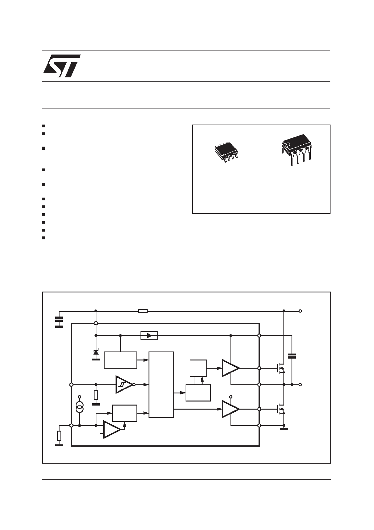
The L6384 is an high-voltage device, manufactured with the BCD”OFF-LINE” technology.It has
L6384
SO8 Minidip
ORDERING NUMBERS:
L6384D L6384
an Half - Bridge Driver structure that enables to
drive N Channel PowerMOS or IGBT. The Upper
(Floating) Section is enabled to work with voltage
Rail up to 600V. TheLogic Inputs are CMOS/TTL
compatible for ease of interfacing with controlling
devices. Matched delays between Lower and Upper Section simplify high frequency operation.
Dead timesettingcan bereadily accomplishedby
means of an external resistor.
BLOCK DIAGRAM
V
CC
1
IN
V
CC
Idt
DT/SD
3
Vthi
2
DETECTION
BOOTSTRAP DRIVER
UV
DEAD
TIME
LOGIC
RS
LEVEL
SHIFTER
LVG
DRIVER
V
CC
HVG
DRIVER
H.V.
V
8
BOOT
C
BOOT
HVG
7
OUT
6
LVG
5
GND
4
D97IN518A
LOAD
May 2000
1/10
L6384
ABSOLUTE MAXIMUM RATINGS
Symbol Parameter Value Unit
Vout Output Voltage -3 toVboot -18 V
Vcc Supply Voltage(*) - 0.3 to 14.6 V
Is Supply Current(*) 25 mA
Vboot Floating Supply Voltage -1 to 618 V
Vhvg Upper Gate Output Voltage -1 to Vboot V
Vlvg Lower Gate Output Voltage -0.3 toVcc +0.3 V
Vi Logic Input Voltage -0.3 toVcc +0.3 V
Vsd Shut Down/Dead Time Voltage -0.3 toVcc +0.3 V
dVout/dt Allowed Output Slew Rate 50 V/ns
Ptot Total Power Dissipation (Tj = 85 °C) 750 mW
Tj Junction Temperature 150 °C
Ts Storage Temperature -50 to 150 °C
(*) The device has an internal Clamping Zenerbetween GND and the Vcc pin, It must not be supplied by a Low Impedence Voltage Source.
Note: ESD immunity for pins 6, 7 and 8 is guaranteedup to 900 V (HumanBody Model)
PIN CONNECTION
IN
V
CC
DT/SD
GND
1
2
3
4 LVG
D97IN519
V
8
7
6
BOOT
HVG
VOUT
5
THERMAL DATA
Symbol Parameter SO8 Minidip Unit
R
th j-amb
Thermal ResistanceJunction to Ambient 150 100 °C/W
PIN DESCRIPTION
N. Name Type Function
1 IN I Logic Input:it is in phase with HVG and in opposition of phase with LGV. It is compatible
2 Vcc I Supply input voltage: there is an internalclamp [Typ. 15.6V]
3 DT/SD I High impedance pin with two functionalities. When pulled lower than Vdt [Typ. 0.5V] the
4 GND Ground
to V
voltage. [Vil Max = 1.5V, Vih Min = 3.6V]
CC
device isshut down. A voltage higher than Vdt sets the dead time between high side gate
driver and low sidegate driver. The dead timevalue can be set forcing a certain voltage
level on the pin or connectinga resistor between pin 3 and ground.
Care must be taken to avoid below threshold spikes on pin 3 that can cause undesired
shut down of the IC. For this reason the connection of the components between pin 3 and
ground has to be as shortas possible. This pin can not be left floating for the same reason.
The pin has not be pulled through a low impedance to V
current source that feeds Rdt. The operative range is:Vdt....270K ⋅ Idt, that allows a dt
range of0.4 - 3.1µs.
, because of thedrop on the
CC
2/10
L6384
PIN DESCRIPTION
(continued)
N. Name Type Function
5 LVG O Low Side Driver Output: the output stage can deliver 400mA source and 650mA sink [Typ.
Values].
The circuitguarantees 0.3V max on the pin (@ I
= 10mA) with VCC> 3V andlower than
sink
the turnon threshold. This allows to omit the bleederresistor connected between the gate
and thesourceof the external mosfet normally used to hold the pin low; thegate driver
ensures lowimpedance also in SD conditions.
6 Vout O Upper Driver Floating Reference: layout care has to be taken to avoid below ground
spikes on this pin.
7 HVG O High Side Driver Output: the output stage can deliver 400mA sourceand 650mA sink
[Typ. Values].
The circuitgurantees 0.3V max between this pin and Vout (@ I
= 10mA) with VCC>3V
sink
and lowerthan the turn on threshold.This allows to omit the bleeder resistorconnected
between thegate and the source of the external mosfet normally used to hold the pin low;
the gatedriver ensures low impedance also in SD conditions.
8 Vboot Bootstrap Supply Voltage: it is the upper driverfloating supply. The bootstrapcapacitor
connected betweenthis pin and pin6 can be fed by an internal structure named ”bootstrap
driver” (a patentedstructure). This structure can replace the externalbootstrap diode.
RECOMMENDED OPERATINGCONDITIONS
Symbol Pin Parameter Test Condition Min. Typ. Max. Unit
Vout 6 Output Voltage Note1 580 V
Vboot -
Vout
fsw Switching Frequency HVG,LVGloadCL= 1nF 400 kHz
Vcc 2 Supply Voltage Vclamp V
T
Note 1: If the condition Vboot - Vout < 18V is guaranteed, Vout can range from -3 to 580V.
8 Floating Supply Voltage Note1 17 V
j
Junction Temperature -45 125 °C
ELECTRICALCHARACTERISTICS
AC Operation(V
Symbol Pin Parameter Test Condition Min. Typ. Max. Unit
ton 1 vs
5,7
tonsd 3 vs
5,7
toff 1 vs
5,7
tr 7,5 Rise Time CL = 1000pF 70 ns
tf 7,5 Fall Time CL = 1000pF 30 ns
= 14.4V;Tj = 25°C)
CC
High/Low SideDriver
Turn-On Propagation Delay
Vout = 0V
R
= 47kΩ
dt
200+dt ns
Shut Down Input Propagation Delay 220 280 ns
High/Low SideDriver
Turn-Off Propagation Delay
Vout = 0V
R
= 47k
dt
Vout = 0V
R
= 146kΩ
dt
Vout = 0V
R
= 270k
dt
Ω
250 300 ns
200 250 ns
170 200 ns
Ω
DC Operation(VCC= 14.4V;Tj = 25°C)
Supply Voltage Section
Vclamp 2 Supply VoltageClamping Is =5mA 14.6 15.6 16.6 V
Vccth1 2 Vcc UV Turn On Threshold 11.5 12 12.5 V
Vccth2 2 Vcc UV Turn Off Threshold 9.5 10 10.5 V
3/10

L6384
DC Operation(continued)
Symbol Pin Parameter Test Condition Min. Typ. Max. Unit
Vcchys 2 Vcc UV Hysteresis 2 V
Iqccu 2 UndervoltageQuiescent SupplyCurrent Vcc ≤ 11V 150 µA
Iqcc 2 Quiescent Current Vin = 0 380 500 µA
Bootstrapped supply Voltage Section
Vboot 8 Bootstrap Supply Voltage 17 V
IQBS Quiescent Current Vout= Vboot;IN= HIGH 200 µA
ILK High VoltageLeakage Current VHVG=Vout= Vboot=
600V
Rdson Bootstrap Driver on Resistance (*) Vcc≥12.5V;IN= LOW 125
High/Low Side Driver
Iso 5,7 Source Short Circuit Current VIN = Vih (tp < 10µs) 300 400 mA
Isi Sink Short Circuit Current VIN = Vil (tp < 10µs) 500 650 mA
Logic Inputs
Vil 2,3 Low Level Logic Threshold Voltage 1.5 V
Vih High LevelLogic Threshold Voltage 3.6 V
Iih High Level Logic Input Current VIN = 15V 50 70
Iil Low Level Logic Input Current VIN = 0V 1
Iref 3 Dead Time Setting Current 28
dt 3 vs
5,7
Dead Time SettingRange (**) Rdt = 47k
Rdt = 146
Rdt = 270k
0.4 0.5
1.5
2.7 3.1
Vdt 3 Shutdown Threshold 0.5 V
10 µA
µ
µ
µ
µs
µs
µ
Ω
A
A
A
s
(V
(*)
(**) Pin 3 is a highimpedence pin. Therefore dt canbe set also forcing a certain voltage V3on this pin. The dead time is the same obtained
is tested in thefollowing way: R
R
DSON
is pin 8 current when V
where I
1
with aRdt if it is: Rdt ⋅ Iref = V
CBOOT=VCBOOT1,I2
.
3
DSON
CC
=
I
1(VCC,VCBOOT1
when V
− V
−(VCC− V
CBOOT1)
)−I2(VCC,V
CBOOT=VCBOOT2
CBOOT2
CBOOT2
)
)
Figure 1. Input/OutputTiming Diagram
IN
SD
HVG
LVG
D99IN1017
4/10

L6384
Figure 2. TypicalRise and Fall Times vs.
Load Capacitance
time
(nsec)
250
200
150
100
50
0
012345C(nF)
For both high and low side buffers @25°C Tamb
D99IN1015
Tr
Tf
BOOTSTRAPDRIVER
A bootstrap circuitryis neededto supply the high
voltage section. This function is normally accomplished by a high voltage fast recovery diode (fig.
4a). In the L6384 a patented integratedstructure
replaces the external diode. It is realized by a
high voltage DMOS, driven synchronously with
the low side driver (LVG), with in series a diode,
as shownin fig. 4b
An internal charge pump (fig. 4b) provides the
DMOS driving voltage .
The diode connected in series to the DMOS has
been added to avoid undesirable turn on of it.
CBOOT selection and charging
To choose the proper C
BOOT
:
value the external
MOS can be seen as an equivalent capacitor.
This capacitor C
gate charge :
The ratio betweenthecapacitorsC
is related to the MOS total
EXT
Q
C
EXT
gate
=
V
gate
andC
EXT
BOOT
is proportionalto the cyclicalvoltage loss .
It hasto be:
C
>>>C
e.g.: if Q
gate
3nF. With C
BOOT
is 30nC and V
= 100nF the drop would be
BOOT
EXT
gate
is 10V, C
EXT
300mV.
If HVG has to be supplied for a long time, the
C
selectionhas to take into accountalso the
BOOT
leakage losses.
e.g.: HVG steady state consumptionis lower than
200µA, so if HVG T
supply 1µCtoC
EXT
is 5ms, C
ON
BOOT
has to
. This charge on a 1µFca-
Figure 3. QuiescentCurrent vs. Supply
Voltage
Iq
(µA)
4
10
3
10
2
10
10
02468101214VS(V)
pacitormeans a voltagedrop of 1V.
The internal bootstrap driver gives great advantages: the external fast recovery diode can be
avoided (it usually has great leakage current).
This structure can work only if V
OUT
GND (or lower) and in the meanwhilethe LVGis
on. The charging time (T
charge
) of the C
the time in which both conditions are fulfilled and
it has to be long enough to chargethe capacitor.
The bootstrap driver introduces a voltage drop
due to the DMOS R
(typical value: 125
DSON
Ohm). At low frequency this drop can be neglected. Anyway increasing the frequency it
must be taken in to account.
The following equation is useful to compute the
drop on the bootstrap DMOS:
= I
V
drop
chargeRdson
where Q
power MOS, R
is the gate charge of the external
gate
is the on resistance of the
dson
bootstrap DMOS, and T
→ V
charge
Q
=
drop
T
charge
is the chargingtime
of the bootstrapcapacitor.
For example: using a power MOS with a total
gate charge of 30nC the drop on the bootstrap
DMOSis about1V, if the T
is
V
drop
hasto betakeninto accountwhenthe voltage
V
drop
droponC
BOOT
30nC
=
⋅ 125Ω ~ 0.8V
5µs
is calculated: if this dropis too high,
charge
is 5µs. In fact:
or the circuit topology doesn’t allow a sufficient
chargingtime,an externaldiodecan be used.
D99IN1016
is close to
gate
R
dson
BOOT
is
5/10

L6384
Figure 4. Bootstrap Driver
D
BOOT
V
S
HVG
LVG
V
V
BOOT
H.V.
OUT
ab
Figure 5. Dead Time vs. Resistance.
3.5
3.0
2.5
2.0
s)
1.5
µ
dt (
1.0
0.5
@ Vcc = 14.4V
Typ.
C
BOOT
TO LOAD
V
V
BOOT
H.V.
OUT
V
S
HVG
LVG
Figure 7. DriverPropagationDelay vs.
Temperature.
400
@ Vcc = 14.4V
300
@ Rdt = 47kOhm
@ Rdt= 270kOhm
@ Rdt = 146kOhm
200
Ton,Toff(ns)
100
Typ.
Typ.
Typ.
C
BOOT
TO LOAD
D99IN1067
0.0
50 100 150 200 250 300
Rdt (kOhm)
Figure 6. Dead Time vs. Temperature.
3
6/10
Typ.
2.5
2
1.5
dt (us)
Typ.
1
0.5
Typ.
0
-45 -25 0 25 50 75 100 125
R=270K
@ Vcc =14.4V
R=146K
R=47K
Tj (°C)
0
-45 -25 0 25 50 75 100 125
Tj (°C)
Figure8.ShutdownThresholdvs.Temperature
1
0.8
@ Vcc = 14.4V
0.6
Typ.
0.4
Vdt (V)
0.2
0
-45 -25 0 25 50 75 100 125
Tj (°C)

L6384
Figure9. VccUV Turn On vs.Temperature
15
14
13
Typ.
12
Vccth1 (V)
11
10
-45 -25 0 25 50 75 100 125
Tj (°C)
Figure10.Vcc UVTurn Off vs.Temperature
13
12
11
Typ.
10
Vccth2 (V)
9
8
-45 -25 0 25 50 75 100 125
Tj (°C)
Figure 11. Output Source Current vs. Tem-
perature.
1000
800
@ Vcc = 14.4V
600
Typ.
400
Current (mA)
200
0
-45 -25 0 25 50 75 100 125
Tj (°C)
Figure12. Output SinkCurrent vs.Temperature
1000
@ Vcc = 14.4V
800
Typ.
600
400
Current (mA)
200
0
-45 -25 0 25 50 75 100 125
Tj (°C)
7/10

L6384
DIM.
MIN. TYP. MAX. MIN. TYP. MAX.
A 3.32 0.131
a1 0.51 0.020
B 1.15 1.65 0.045 0.065
b 0.356 0.55 0.014 0.022
b1 0.204 0.304 0.008 0.012
D 10.92 0.430
E 7.95 9.75 0.313 0.384
e 2.54 0.100
e3 7.62 0.300
e4 7.62 0.300
F 6.6 0.260
I 5.08 0.200
L 3.18 3.81 0.125 0.150
Z 1.52 0.060
mm inch
OUTLINE AND
MECHANICAL DATA
Minidip
8/10

L6384
DIM.
MIN. TYP. MAX. MIN. TYP. MAX.
A 1.75 0.069
a1 0.1 0.25 0.004 0.010
a2 1.65
a3 0.65 0.85 0.026 0.033
b 0.35 0.48 0.014 0.019
b1 0.19 0.25 0.007 0.010
C 0.25 0.5 0.010 0.020
c1 45° (typ.)
D (1) 4.8 5.0 0.189 0.197
E 5.8 6.2 0.228 0.244
e 1.27 0.050
e3 3.81 0.150
F (1) 3.8 4.0 0.15 0.157
L 0.4 1.27 0.016 0.050
M 0.6 0.024
S8°(max.)
(1) D andF do not include moldflash or protrusions. Mold flash or
potrusions shallnot exceed0.15mm(.006inch).
mm inch
0.065
OUTLINE AND
MECHANICAL DATA
SO8
9/10

L6384
Information furnished is believed to be accurate and reliable. However, STMicroelectronics assumes no responsibility for the consequences
of use of such information nor for any infringement of patents or other rights of third parties which may result from its use. No license is
granted by implication or otherwise under any patent or patent rights of STMicroelectronics. Specification mentioned in this publication are
subject to change without notice. This publication supersedes and replaces all information previously supplied. STMicroelectronics products
are not authorized for use as critical components in life support devices or systems without express written approval of STMicroelectronics.
The ST logo is a registeredtrademark of STMicroelectronics
2000 STMicroelectronics – Printed in Italy – All Rights Reserved
STMicroelectronics GROUP OFCOMPANIES
Australia - Brazil - China- Finland - France - Germany - Hong Kong - India - Italy - Japan - Malaysia - Malta - Morocco -
Singapore - Spain - Sweden - Switzerland - UnitedKingdom - U.S.A.
http://www.st.com
10/10
 Loading...