

Page 1
INDUSTRIAL QUAD LINE DRIVER
FOUR INDEPENDENT LINE DRIVERS WITH
100 mAUP TO35VOUTPUTS
INPUT SIGNALS BETWEEN -7V AND +35V,
WITHPRESETTABLETHRESHOLD
PUSH-PULL OUTPUTS WITH THREE STATE
CONTROL AND TRUE ZERO CURRENT BETWEENV
CURRENT LIMITING ON EACH OUTPUT EFFECTIVE IN THE FULL ”GROUND TO V
OUTPUTVOLTAGERANGE
OUTPUT VOLTAGE CLAMP TO V
GROUND
OVERTEMPERATURE AND UNDERVOLTAGE PROTECTIONS
DIAGNOSTIC FOR OVERTEMPERATURE,
UNDERVOLTAGEAND OVERCURRENT
PRESETTABLE DELAY FOR OVERCURRENTDIAGNOSTIC
HIGH SPEED OPERATION: UP TO 300kHz
WITH 35VSWING
ANDGROUND
S
S
S AND TO
ADVANCE DATA
”
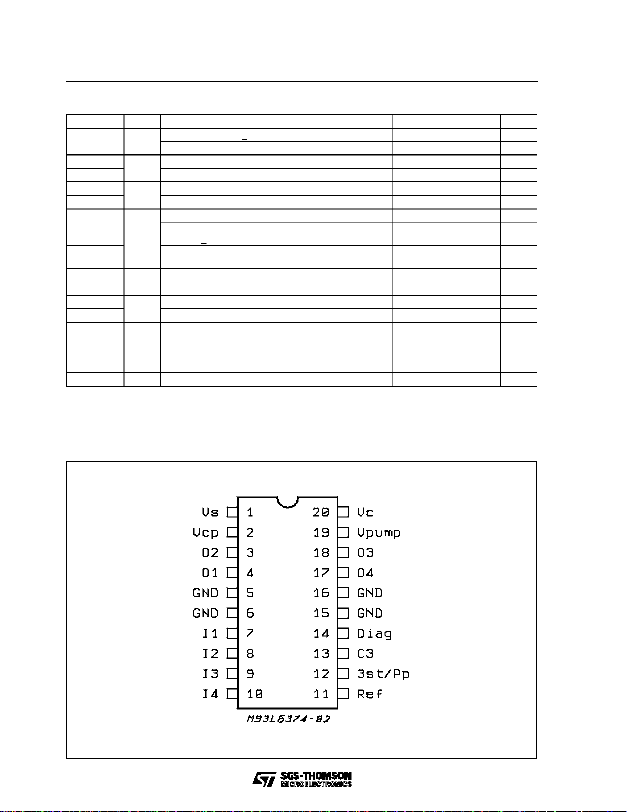
POWERDIP 16+2+2 SO 16+2+2
ORDERING NUMBER: L6374DP (POWERDIP16+2+2)
L6374FP (SO16+2+2)
DESCRIPTION
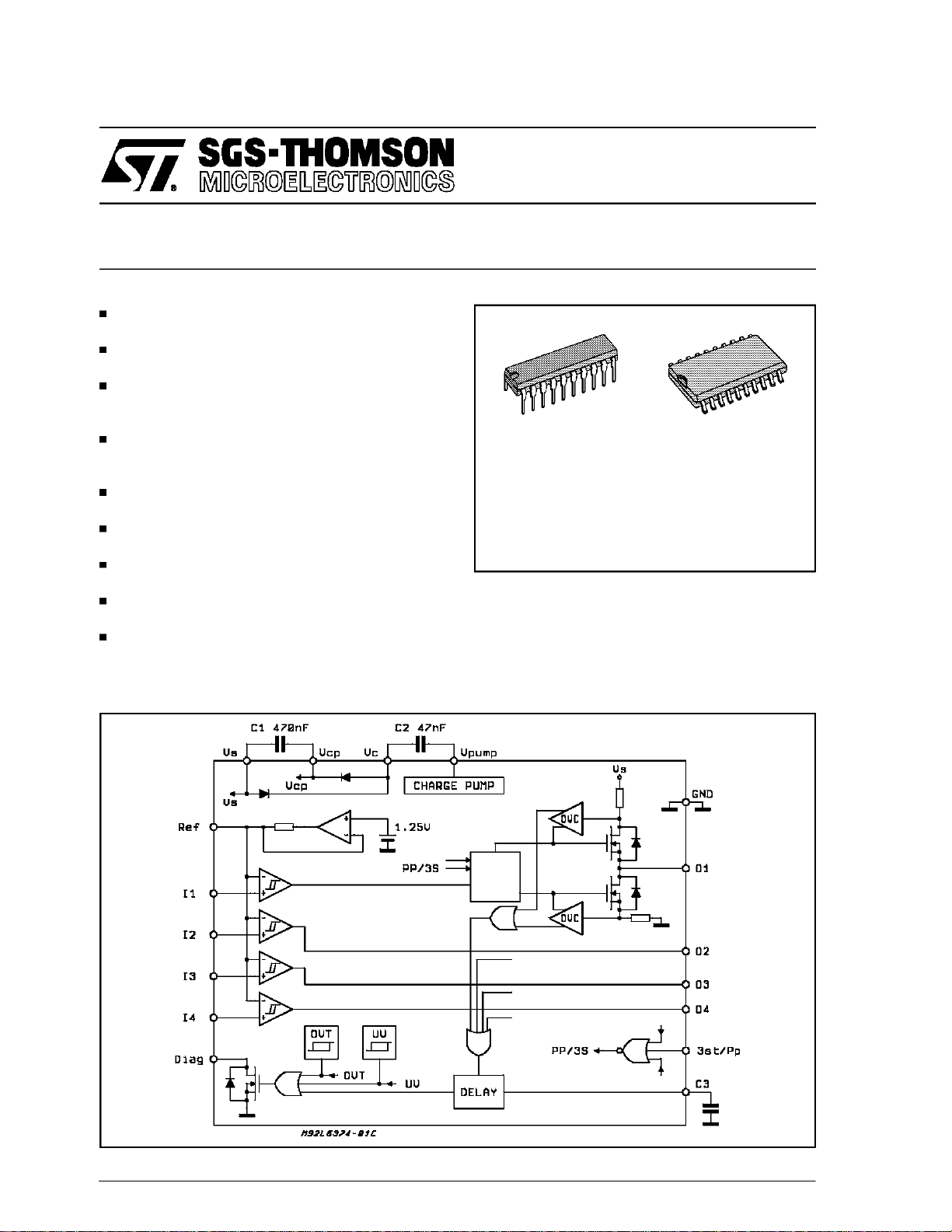
The L6374 is especiallydesignedto be used as a
line driver in industrial control systems based on
the 24V signal levels (IEC1131, 24VDC).
L6374
BLOCK DIAGRAM
December 1994
This is advanced information on a new product now in development orundergoing evaluation.Details are subject to change without notice.
1/13
Page 2
L6374
ABSOLUTE MAXIMUM RATINGS
Symbol Pin Parameter Value Unit
S 1 Supply Voltage(t
V
Supply Voltage(DC) 40 V
ilog 12, 13 Logic Input Voltage (DC) -0.3 to 7 V
V
ilog Logic Input forced current, per pin ±1mA
I
i7, 8,
I
i ChannelInput Voltage - 7 to35 V
V
out 3, 4,
I
9, 10
17, 18
out OutputVoltage (forced, not resulting from an inductive
V
Channel Input Current (forced) ±2mA
Output Current (forced, apart from inductive load) ±100 mA
Output Current (forced, apart from inductive load)
same t
< 10ms
W
kick)
I
set 11 Setting pin forced current ±1mA
set Setting pin forced voltage -0.3 to 5 V
V
diag 14 External voltage -0.3 to 35 V
V
diag Externallyforced current -10 to 10 mA
I
C3 13 Voltage on the delay capacitor, externally forced -0.3 to 4.5 V
V
op Ambient temperature, operating range -25 to 85 °C
T
j Junction temperature, operatingrange (see
T
Overtemperature Protection)
T
stg Storage temperature -55 to 150 °C
< 10ms) 50 V
W
±1A
-0.3 to VS +0.3 V
-25 to 125 °C
PIN CONNECTION (Top view)
2/13
Page 3
ELECTRICALCHARACTERISTICS (VS = 24V; Tj = -25 to 125°C; unless otherwise specified.)
DC OPERATION
Symbol Pin Parameter Test Condition Min. Typ. Max. Unit
S 1 Supply Voltage 10.8 35 V
V
sh UV UpperThreshold 9 10.8 V
V
ys1 UV Hysteresis 250 450 650 mV
H
qsc Quiescent Current Outputs Open 3 5 mA
I
ref 11 Input Comparators Reference
V
Voltage
I
ref
Sink/Source Current on
Reference Pin
th 7, 8,
V
il Input Low Level V
V
ih Input High Level V
V
i Input Voltage(Operative Range) -7 35 V
V
bias Input Bias Current 0 < Vi <VS -1 1 µA
I
ys2 Input ComparatorsHysteresis See Analog Inputs Sections 100 200 350 mV
H
h OVT Upper Threshold 170 °C
T
T OVT Hysteresis 20 °C
H
sc 3, 4,
I
on Internal Voltage Drop @ Rated
V
17,18
Comparator Threshold with
9, 10
External Bias
Current Limit Vi =-7toVS;Vout = 0 to VS; 110 200 300 mA
Current
I
lkg
in 12 Push-Pull Mode Request -0.2 0.8 V
V
Output 3-State Leakage Current V
3-State Mode Request 2 5.5 V
in Input Current V
I
dlkg 14 Diagnostic OutputLeakage Diagnostic Off; V
I
diag Diagnostic OutputVoltage Drop I
V
Reference pin Floating 1.05 1.25 1.35 V
V
= 0V -30 -20 -10 µA
ref
=5V 10 20 30 µA
V
ref
VS = 9 to 12V -0.2 2.0 V
S = 12 to 35V -0.2 5.0 V
V
Externally Biased -7 V
REF
REF
-0.2
Pin V
Floating -7 0.8 V
REF
Externally Biased V
REF
REF
35 V
+0.2
Pin V
i = -7V -1 -0.5 -0.1 mA
V
Iout = ±100mA; Sourced @ High
Floating 2 35 V
REF
400 600 mV
Output, Sunk @ Low Output
T
= 125°C
j
Same, T
out
i
diag
=25°C 250 400 mV
j
= 0 to V
S
-25 25 µA
=0V 10 25 µA
= 24V 5 µA
diag
=5mA 200 500 mV
L6374
V
AC OPERATION (VS = 10.8 to 35V; Tj = -25 to 125°C; I
= 100mA; unless otherwise specified; see
out
switchingwaveforms diagrams)
Symbol Pin Parameter Test Condition Min. Typ. Max. Unit
dr 7to4
t
8to3
df Delay Time on Falling Edge Rl to ground 500 1000 ns
t
r 3,4,
t
9to18
10to17
17, 18
f Fall Time Rl to ground 150 300 ns
t
Delay Time on Rising Edge R
l to ground 1000 1500 ns
to V
R
l
S
to V
R
l
S
500 1000 ns
1000 1500 ns
Rise Time Rl to ground 120 250 ns
to V
R
l
S
to V
R
l
S
120 250 ns
150 300 ns
3/13
Page 4
L6374
THERMAL DATA
Symbol Parameter DIP20 SO20 Unit
th j-pin Thermal Resistance, Junction to Pin 12 17 °C/W
R
th j-amb1 Thermal Resistance, Junction to Ambient (see Thermal
R
R
th j-amb2 Thermal Resistance, Junction to Ambient (see Thermal
Characteristics)
Characteristics)
40 65 °C/W
50 80 °C/W
THERMAL CHARACTERISTICS
R
th j-pins
POWERDIP. The thermalresistanceis referred
to the thermalpath from thedissipatingregion
on the top surface of the siliconchip, to the
points alongthe four central pins of the package, at a distanceof 1.5 mm awayfrom the
stand-offs.
SO. Similarly, the referencepoint is the knee
on the four central pins, where the pins areupwardly bent and the solderingjoint with the
PCB footprintcan be made.
R
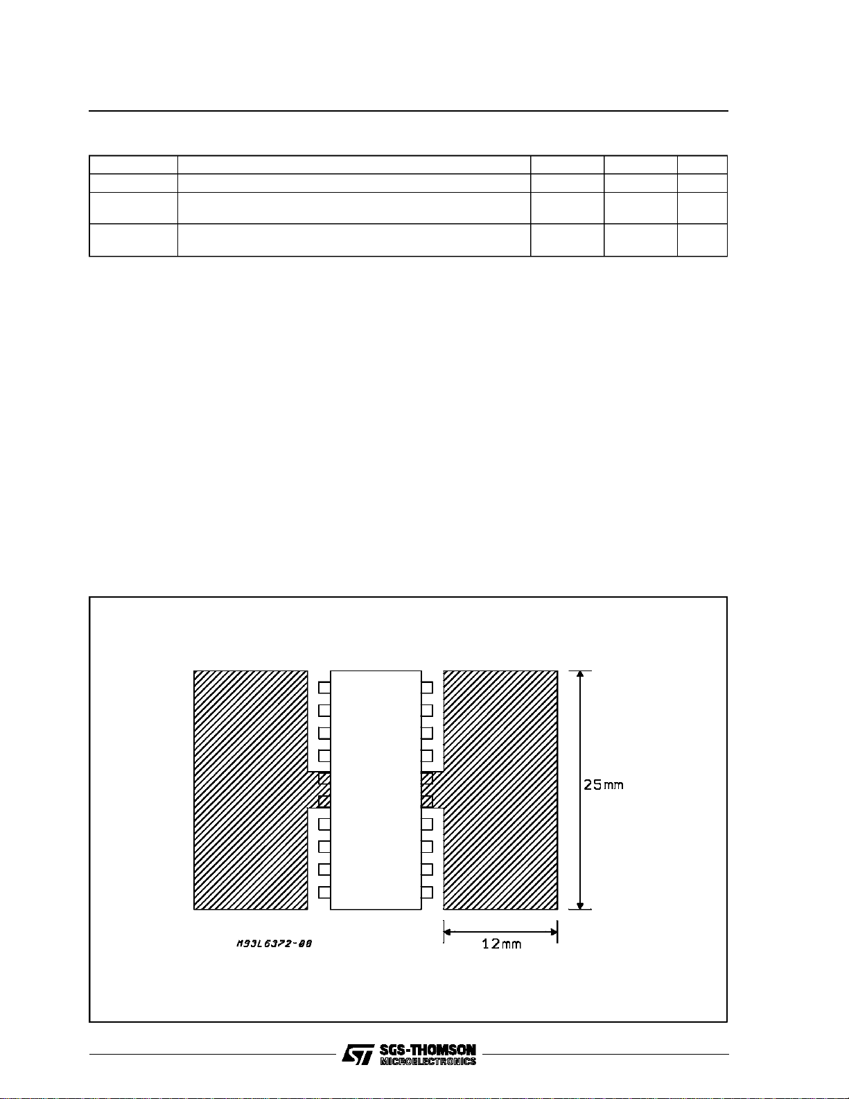
th j-amb1
If a dissipatingsurface, thick at least 35 µm,
and with a surfacesimilar or bigger thanthe
one shown, iscreated making use of the
printed circuit.
Figure1: Printed Heatsink
Such heatsinkingsurface isconsidered on the
bottom side of an horizontalPCB (worst case).
R
th j-amb2
If the power dissipatingpins (the four central
ones), as well as the others, have aminimum
thermalconnection with the externalworld
(very thin strips only) so thatthe dissipation
takesplace through still air and through the
PCB itself.
It is the same situationof pointabove, without
any heatsinkingsurface createdon purposeon
the board.
Additionaldata for the PowerDip package can be
foundin:
ApplicationNote 9030:
Thermal Characteristicsof the PowerDip
20,24PackagesSolderedon 1,2,3 oz.
CopperPCB
4/13
Page 5

L6374
OVERTEMPERATUREPROTECTION(OVT)
If the chip temperature exceeds T
(measured in
h
a central position in the chip) the chip deactivates
itself.
The followingactions are taken:
- all the output stages are forced in the ”three
state” condition, i.e. are disconnected from
the output pins; only the clamping diodes at
the outputsremain active;
- the signal Diag is activated(active low).
Normaloperation is resumed as soonas (typically
after some seconds) the chip temperature monitored goes back below T
h-HT
.
The different upper and lower thresholds with
hysteretic behavior, assure that no intermittent
conditionscan be generated.
UNDERVOLTAGE PROTECTION(UV)
The supply voltageis expectedto range from 11V
to 35V, evenif its referencevalue is considered to
be 24V.
In this rangethe L6374 operatescorrectly.
Below 10.8V the overall system has to be considerednot reliable.
Consequently the supply voltage is monitored
continuously and a signal, called UV, is internally
generatedand used.
The signal is ”on” as long as the supply voltage
does not reach the upper internal threshold of the
comparator(called Vsh). The UV signal disap-
V
s
pearsabove V
.
sh
Once the UV signal has been removed, the supply voltage must decrease below the lower
threshold (i.e. below V
sh-Hys1
) before it is turned
on again.
The hysteresis H
is provided to prevent inter-
ys1
mittent operation of the device at low supply voltages that may have a superimposed ripple
aroundthe averagevalue.
The UV signal inhibits the outputs,puttingthem in
three-state, but has no effect on the creation of
the reference voltages for the internal comparators, nor on the continuous operation of the
charge-pumpcircuits.
DIAGNOSTIC LOGIC
The situations that are monitored and signalled
with the Diag output pin are:
- current limit (OVC) in action; there are 8 individual current limiting circuits, two per each
output, i.e. one per every output transistor;
they limit the current that can be either sourced or sunk from each output, to a typical
value of 150mA,equal for all of them;
- undervoltageprotection (UV);
- overtemperatureprotection (OVP);
The diagnostic signal is transmitted via an open
drain output (for ease of wired-or connection of
several such signals) and a low level represents
the presence of at least one of the monitoredconditions,mentionedabove.
PROGRAMMABLE DELAY
The current limiting circuits can be requested to
perform even in absence of a real fault condition,
for a short period, if the load is of capacitive nature or if it is a filament lamp (that exhibits a very
lowresistanceduring theinitial heatingphase).
To avoid the forwarding of misleading, short diagnostic pulses in coincidence with the intervention
of the current limiting circuits when operating on
capacitive loads, a delay of about 5µs is inserted
on the signal path, between the ”OR” of the currentlimit signalsanditsuse as externaldiagnostic.
It takes about 1µs to charge (or discharge) by
24V a capacitorof 5nFwith a currentof 120mA .
To implement longer delays (from the intervention
of one of the current limiting circuits to the activation of the diagnostic) an external capacitor can
be connectedbetween pin C3 and ground(pin C3
isotherwise left open).
Thedelay shall then be determinedby the ratio of
about 10 pF/µs, using the value of the capacitanceconnected to the pin.
ANALOG INPUTS(I1,I2,I3,I4)
The input stage of each channel is a high impedence comparator with built-in hysteresis
(200mV) for high noise immunity. Each comparator has one input connected to all the others and
tied to a commonpin Ref (Pin 11). If thispin is left
floating an internal precise band gap voltage reference (1.25V) is applied, otherwise these inputs
can be externally programmed by connecting an
external voltage source (from 0 to 5V) and the
currenton thispin is internallylimited to ±20µA.
Theother input pin of each comparatorcan swing
from-7 to 35V.
For this reason it has been implemented the
structure shown in Figure 2 and the device can
alsobe usedas line receiver.
When the input voltage is negative, the current is
internally limited by a 15kΩ resistor as shown in
Figure 2. High and low input thresholds can be
obtained by adding and subtracting half of the
hysteresisto the voltageof pin Ref(see Figure 3).
Figure2: Equivalentinput circuit
5/13
Page 6

L6374
Figure3: Input ComparatorThreshold
H
V
out
V
s
ys2
22
3 STATE/ PUSH-PULL INPUT
The input 3st/Pp is instead intended for a digital
incomingsignal. It has an internal thresholdset at
1.26V; an internal bias circuit (10µA typical) simulates a high level (three-state) if the pin is disconnected.
THE SWITCHING OF THEOUTPUT STAGE
The cross conduction of the two transistors of an
output stage of the L6374 would be significantly
noisy, because the transistors here can carry
peak currents in excess of 100mA, and even
more in the few nanoseconds before the current
limitingcircuits are reallyeffective.
H
ys2
V
ref
D94IN073
V
i
Consequently the device has been designed so
as to avoid such cross conduction. At every
switching transition, first of all the transistor in
conduction is turned off. Then, after a safe interval of around 200ns, the other transistor is turned
on.
When analyzing the switching cycle, and the associated switching times, it is useful to identify
somesubsequent phases:
- delay from theinput pin to the output reaction;
- off transitionin the output stage;
- dead time;
- on transitionin the output stage.
Figure 4 helps understand such sequence. In
Figure4: V
= 35V,350Ω connectedto VS/2.
S
6/13
Page 7

L6374
fact, with a purelyresistiveload connected to Vs/2
no parasiticelements interferesignificantly.
The waveformcan be significantlyless easy to interpret if the load has not the perfect symmetryof
that case, as showed below. For instance, it is
enough to connectthe resistiveload to ground, or
– as figure 5 and 6 – show to hide some of
to V
s
the switching phasesdescribed.
If the load is connected to ground, the waveform
stays stuck to ground as long as the outputstage
is in high impedance; viceversa when the load is
connected to V
the waveform will linger close to
s
the supplyvoltage as longas possible.
If an output load made of an inductorand a resistor in series is used, the inductive kick at the beginning of every output transition generates the
equivalent effect of an ”anticipated” switching
when the inductor can discharge; while the
switching looks ”delayed” if the output transition
tends to initiatea chargingphase (see figure 7).
With a load almost free from parasitic elements,
the waveforms resemble the ones of the purely
Figure5: V
= 35V,350Ω connectedto ground.
S
resistivecases.
Witha real, morecomposite load, the effect of the
inductive kick in comparison to the resistive load,
wouldbe moreapparent.
With a capacitor and a resistor in parallel as a
load, another type of waveform can be seen (reported in figure8).
As long as the output stage stays in the transient
high impedance state, the output voltage will follow the classic exponential law of an RC relaxation.
As soon as the other transistoris switchedon and
takes charge, the waveform is quickly forcibly
broughtto its steady state value.
From the above it is possible to see how the
switching times, inherently very fast, of the output
stages,may be difficult to identify in a waveformif
the output load is not accurately taken into consideration.
Figure 9 show typical switching waveform for inputs and outputs.
7/13
Page 8

L6374
Figure6. VS=35V, 350Ω connected to VS.
Figure7. V
=35V, 350Ω & 1mH connected to ground.
S
8/13
Page 9

Figure8: VS= 35V,350Ω || 1nFconnected to ground.
L6374
Figure9: SwitchingWaveforms.
In
50% 50%
Out
t
dr
90% 90%
10% 10%
t
r
t
df
t
f
D94IN074
t
t
9/13
Page 10

L6374
APPLICATIONNOTE
It is recommended not to leave the Ref pin
(pin 11) floating: if not used with an external voltage reference, it is better to connect an external
capacitor (of at least 10nF) between this pin and
ground.
This capacitorfilters the voltage referenceagainst
voltage spikesthat can be generatedby the commutationof the output stages.
This is very common using capacitive loads: in
fact, the initial transient of such loads behaves
like a short circuit, so the current flowing through
the outputspresents very high spikes.
Moreover, if the device is used as a line receiver.
(i.e. the input signals can go below ground) it is
required not to leave the Ref pin (pin 11) floating:
in this case, the pin can be connected to ground
or to a fixed external voltage reference.
10/13
Page 11

DIP20 PACKAGEMECHANICAL DATA
L6374
DIM.
MIN. TYP. MAX. MIN. TYP. MAX.
a1 0.51 0.020
B 0.85 1.40 0.033 0.055
b 0.50 0.020
b1 0.38 0.50 0.015 0.020
D 24.80 0.976
E 8.80 0.346
e 2.54 0.100
e3 22.86 0.900
F 7.10 0.280
I 5.10 0.201
L 3.30 0.130
Z 1.27 0.050
mm inch
11/13
Page 12

L6374
SO20PACKAGE MECHANICAL DATA
DIM.
MIN. TYP. MAX. MIN. TYP. MAX.
A 2.65 0.104
a1 0.1 0.3 0.004 0.012
a2 2.45 0.096
b 0.35 0.49 0.014 0.019
b1 0.23 0.32 0.009 0.013
C 0.5 0.020
c1 45(typ.)
D 12.6 13.0 0.496 0.512
E 10 10.65 0.394 0.419
e 1.27 0.050
e3 11.43 0.450
F 7.4 7.6 0.291 0.299
L 0.5 1.27 0.020 0.050
M 0.75 0.030
S 8 (max.)
mm inch
12/13
Page 13

L6374
Information furnished is believed to be accurate and reliable. However, SGS-THOMSON Microelectronics assumes no responsibility for the
consequences of use of such information nor for any infringement ofpatents or other rights of third parties which may result from its use. No
license is granted by implication or otherwise under any patent or patent rights of SGS-THOMSON Microelectronics. Specifications mentioned in this publication are subject to change without notice. This publication supersedes and replaces all information previously supplied.
SGS-THOMSON Microelectronics products are not authorized for use as critical components in life support devices or systems withoutexpress written approval of SGS-THOMSON Microelectronics.
1994 SGS-THOMSON Microelectronics - All RightsReserved
Australia - Brazil- France - Germany - Hong Kong - Italy- Japan - Korea - Malaysia -Malta - Morocco -The Netherlands
Singapore - Spain - Sweden - Switzerland- Taiwan -Thaliand - United Kingdom - U.S.A.
SGS-THOMSON Microelectronics GROUP OF COMPANIES
13/13
 Loading...