

L6370
2.5A HIGH-SIDE DRIVER
INDUSTRIALINTELLIGENT POWER SWITCH
2.5A OUTPUT CURRENT
9.5V TO35V SUPPLY VOLTAGE RANGE
INTERNALCURRENT LIMITING
THERMALSHUTDOWN
OPENGROUNDPROTECTION
INTERNALNEGATIVE VOLTAGE CLAMPING
TOV
- 50VFOR FAST DEMAGNETIZATION
S
DIFFERENTIAL INPUTS WITH LARGE COMMON MODE RANGE AND THRESHOLD
HYSTERESIS
UNDERVOLTAGELOCKOUTWITHHYST ERESIS
OPENLOAD DETECTION
TWODIAGNOSTICOUTPUT S
OUTPUTSTATUS LEDDRIVER
NON DISSIPATIVE SHORT CIRCUIT PRO-
TECTION
PROTECTIONAGAINST AND SURGE TRAN-
SIENT (IEC 801-5)
IMMUNITY AGAINST BURST TRANSIENT
(IEC801-4)
ESD PROTECTION (HUMAN BODY MODEL
2KV)
±
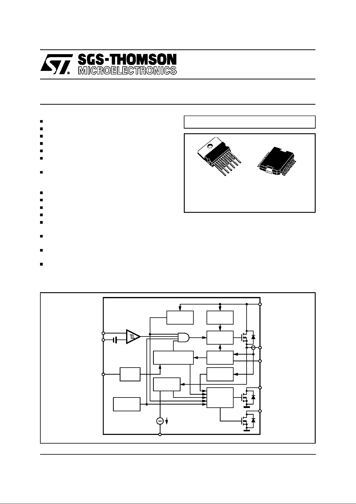
BLOCK DIAGRAM
MULTIPOWER BCD TECHNOLOGY
MULTIWATT11(in line)
ORDERINGNUMBERS: L6370L (MULTIWATT11)
PowerSO20
L6370D (PowerSO20)
DESCRIPTION
The L6370 is a monolithic Intelligent Power
Switch in Multipower BCD Technology, for driving
inductive or resistive loads. An internal Clamping
Diode enables the fast demagnetizationof inductive loads. Diagnostic for CPU feedback and extensive use of electricalprotections make this device extremely rugged and specially suitable for
industrialautomation applications.
March 1997
IN+
IN-
ON-DELAY
INPUT
1.4V
OSC
THERMAL
PROTECTION
+
-
NON DISSIPATIVE
SHORT CIRCUIT
OUTSTATUS
3mA
OUTPUT STATUS
UNDER
VOLTAGE
CHARGE
PUMP
DRIVER
CURRENT
LIMITATION
OPEN LOAD
DETECTION
DIAGNOSTIC
D95IN208D
V
S
OUT
RSC
DIAG1
DIAG2
1/10
L6370
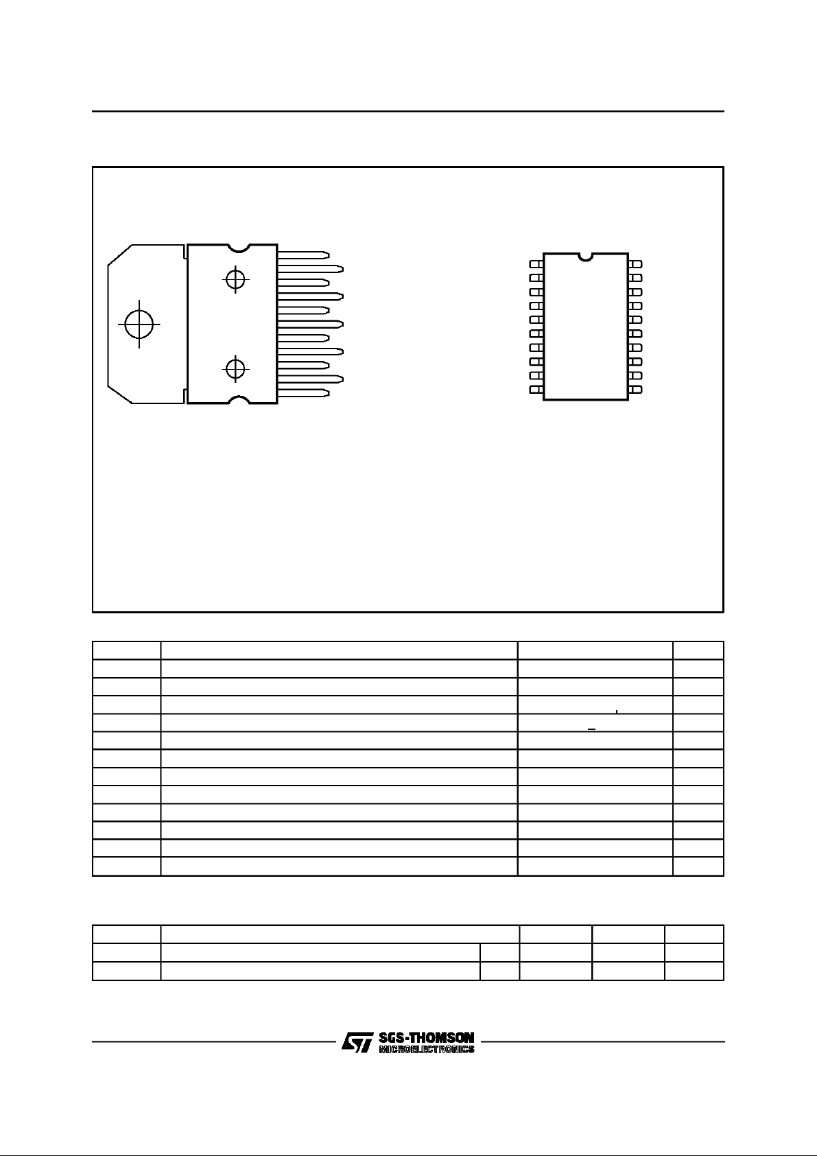
PIN CONNECTION (Topview)
11
10
9
8
7
6
5
4
3
2
1
D95IN209A
OUTPUT
SUPPLY VOLTAGE
OUTPUT
RSC
ON-DELAY
GND
OUTPUT STATUS
INPUT INPUT +
DIAGNOSTIC 2
DIAGNOSTIC 1
GND
OUTPUT
OUTPUT
ON-DELAY
SUPPLY VOLTAGE
N.C.
OUTPUT
OUTPUT N.C.
GND GND
2
3
4
5
6
7
8
9
10
20
19
18
17
16
15
14
13
12
11
GND1
OUTPUT STATUS
INPUT INPUT +
N.C.SUPPLY VOLTAGE
DIAGNOSTIC 2
DIAGNOSTIC 1
RSC
D95IN210B
Note: Outputpins must be must be connected externally to the package touse all leadsfor the outputcurrent(Pin9 and11 for Multiwatt
package, Pin 2, 3, 8 and 9 for PowerSO20 package).
ABSOLUTE MAXIMUM RATINGS (Pinnumberingreferredto Multiwatt package)
Symbol Parameter Value Unit
V
V
S–VO
V
I
V
V
I
P
T
T
E
S
od
od
I
O
tot
op
stg
Supply Voltage (Pin 10) (TW< 10ms) 50 V
Supplyto Output Differential Voltage.Seealso VCl(Pins10 - 9) internally limited V
Externally Forced Voltage (Pin7) -0.3 to 7 V
Externally Forced Voltage (Pin7) +1 mA
Input Voltage (Pins 3/4) -10 to VS +10 V
i
Differential Input Voltage (Pins 3 - 4) 43 V
i
Input Current (Pins 3/4) 20 mA
i
Output Current (Pin 9). See also ISC (Pin 9) internally limited A
Power Dissipation.See also THERMAL CHARACTERISTICS. internally limited W
Operating Temperature Range (T
) -25 to +85 °C
amb
Storage Temperature -55 to 150 °C
Energy Induct.Load TJ=85°C1J
I
THERMAL DATA
Symbol Description Multiwatt PowerSO20 Unit
Thermal Resistance Junction-case Max. 1.5 1.5 °C/W
Thermal Resistance Junction-ambient Max. 35 – °C/W
2/10
R
th j-case
R
th j-amb

PIN FUNCTION (pinnumbering referred to Multiwattpackage)
N. Name Function
1 DIAG1 DIAGNOSTIC 1 output. This open drain reports the IC workingconditions. (See
Diagnostic truth table)
2 DIAG1 DIAGNOSTIC 2 output. This open drain reports the IC workingconditions. (See
Diagnostic truth table)
3 IN - Comparator non inverting input
4 IN+ Comparator inverting input
5 OUTSTATUS This current source output is capable of drivinga LED to signal the status of the output
pin. The pin is active (source current) when the output pin is considered high (See fig 1)
6 GND Ground
7 ON-DELAY Programmable ON time interval duration during short circuit operation
8 RSC Current limitation setting.
9 OUTPUT High Side output with built-in current limitation
10 V
S
Supply Volatge Input, the valueof the supplyvoltage is monitored to detect under voltage
condition
11 OUTPUT High Side output with built-in current limitation
ELECTRICALCHARACTERISTICS (VS= 24V; TJ= –25 to +125°C, unless otherwise specified)
Symbol Parameter Test Condition Min. Typ. Max. Unit
V
smin
V
s
I
q
V
sth1
V
sth2
V
shys
I
sc
V
don
I
oslk
V
ol
V
cl
I
old
V
id
I
ib
V
ith
V
iths
R
id
I
ilk
Supply Voltage for Valid
I
> 0.5mA ; V
diag
= 1.5V 4 35 V
dg1
Diagnostics
Supply Voltage (operative) 9.5 24 35 V
Quiescent Current
I
out=Ios
=0
V
V
il
ih
0.8
3
1.4
5
Undervoltage Threshold 1 (See fig. 1), Tamb = 0 to +85°C 8.5 9 9.5 V
Undervoltage Threshold 2 8 8.5 9 V
Supply Voltage Hysteresis 300 500 700 mV
Short Circuit Current VS= 9.5 to 35V; RL=2
Output Voltage Drop I
5kΩ <R
0<R
out
I
out
< 30kΩ
SC
<5kΩ 2.6 3.2 4 A
SC
= 2.0A Tj=25°C
T
= 125°C
j
= 2.5A Tj=25°C
T
= 125°C
j
Ω
(kΩ)A
15/R
SC
200
320
250
400
280
440
350
550
Output Leakage Current Vi=Vil;Vo= 0V 500 µA
Low State Out Voltage Vi=Vil;RL=∞ 0.8 1.5 V
Internal Voltage Clamp (VS-VO)IO=1A
48 53 58 V
Single Pulsed: Tp =300µs
Open Load Detection Current Vi=Vih;T
Common Mode Input Voltage
VS= 18 to 35V –7 15 V
= 0 to +85°C136mA
amb
Range (Operative)
Input Bias Current Vi= –7 to 15V; –In = 0V –250 250 µA
Input Threshold Voltage V+In > V–In 0.8 1.4 2 V
Input Threshold Hysteresis
V+In > V–In 50 400 mV
Voltage
Diff. Input Resistance 0 < +In < +16V; –In= 0V
–7 < +In < 0V ; –In = 0V
Input Offset Current V+In = V–In +Ii
0V < V
<5.5V –Ii
i
–In = GND +Ii
0V < V+In <5.5V –Ii –250
+In = GND +Ii
0V < V–In <5.5V –Ii
–20
–75 –25
–100
–50
400
150
+10
–125
–30
–15
+20 µA
+50
L6370
mA
mA
mV
mV
mV
mV
K
Ω
KΩ
A
µ
A
µ
µA
µA
µA
3/10

L6370
ELECTRICALCHARACTERISTICS (continued)
Symbol Parameter Test Condition Min. Typ. Max. Unit
V
oth1
Output Status Threshold 1
Voltage
V
oth2
Output Status Threshold 2
Voltage
V
ohys
Output Status Threshold
Hysteresis
I
osd
V
osd
Output Status Source Current V
Active Output Status Driver
Drop Voltage
I
oslk
Output Status Driver Leakage
Current
V
I
dgl
dglk
Diagnostic Drop Voltage D1 /D2= L ; I
Diagnostic Leakage Current D1 / D2=H ; 0 < Vdg < V
SOURCE DRAIN NDMOS DIODE
V
fsd
I
fp
t
rr
t
fr
Forward OnVoltage @ I
Forward Peak Current t = 10ms; d = 20% 6 A
Reverse Recovery Time If= 2.5A di/dt = 25A/µs 200 ns
Forward Recovery Time 100 ns
THERMAL CHARACTERISTICS
Θ Lim Junction Temp. Protect. 135 150 °C
T
Θ
Note Vil< 0.8V, Vih> 2V @ (V+In > V–In)
Thermal Hysteresis 20
H
AC OPERATION(pin numberingreferred to Multiwatt package)
(See fig. 1) 4.5 5 5.5 V
(See fig. 1) 4 4.5 5.0 V
(See fig. 1) 300 500 700 mV
out>Voth1;Vos
Vs – Vos;Ios= 2mA
T
= 0 to+85°C
amb
V
out<Voth2;Vos
V
= 9.5 to 35V
S
D1/D2=L; I
= 2.5V 2 4 mA
1.5 3 V
diag
diag
=0V
= 0.5mA
= 3mA
40
250
s
25 µA
5
VS= 9.5 to 35V
= 2.5A 1 1.5 V
fsd
mV
mV
µ
C
°
A
Symbol Pin Parameter Test Condition Min. Typ. Max. Unit
-t
t
r
t
d
9vs 4 Rise or Fall Time VS= 24V; RI=70Ω;Rlto
f
9 vs 3 Delay Time 5 µs
ground
20 µs
dV/dt 9, 11 Slew Rate (Rise and Fall Edge) 0.7 1 1.5 V/µs
t
ON
7 On time during Short Circuit
50pF <C
< 2nF 1.28 µs/pF
DON
Condition
t
OFF
Of time during hort Circuit
64 t
Condition
f
max
Maximum Operating
25 KHz
Frequency
Figure 1: Output Status Hysteresis
V
shys
V
oth2
V
oth1
D95IN211A
V
OUT
ON
4/10

Figure 2: UndervoltageComparator Hysteresis
V
L6370
shys
V
oth1
V
oth2
D95IN212
V
s
Figure 3: Switching Waveforms
V
in
50% 50%
D94IN127A
t
t
t
d
V
out
90% 90%
50% 50%
10% 10%
t
r
t
d
t
f
DIAGNOSTICTRUTH TABLE
Diagnostic Conditions Input Output Diag1 Diag2
Normal Operation L
H
Open Load Condition (I
)L
o<Iold
H
Short to V
S
L
H
Short Circuit to Ground (I
O=ISC
) (**)
H H (*)
(pin ON-DELAY grounded)
Output DMOS Open L
H
Overtemperature L
H
Supply Undervoltage (V
S<Vsth2
)L
H
(*) According to the intervention of the current limitingblock.
(**) A cold lamp filament, or a capacitive load may activate the current limiting circuit ofthe IPS, when the IPSis initially turnedon.
L
H
L
H
H
H
H
H
H
L
L
L
H
L
L
L
L
L
L
L
H
H
L
H
H
L
L
H
H
H
H
H
H
H
H
H
H
L
L
L
L
5/10

L6370
INPUT SECTION
The input section is an high impedance differential stage with high common and differentialmode
range. There’s built-in offset of +1.4V (typical
value) and an hysteresis of 400mV (maximum
value), to ensure high noiseimmunity.
DIAGNOSTICLOGIC
The operatingconditions of the deviceare permanently monitored and the following occurences
are signalled via the DIAG1/DIAG2 open-drain
output pins:
-ShortCircuit versus ground.
A current limiting circuit fixes at Isc = 3.2A
(typical value) the maximum current that can
be sourced from the OUTPUT pin (for more
detailssee shortcircuit operation section).
- ShortCircuitversusVs.
- UnderVoltage(UV)
- Over Temperature(OVT)
- Open Load, if the output current is less than
3mA(typical value).
- OutputDMOS Open
accordingto the diagnosticTruth Table:
erationis resumed.
The t
and 2.56ms for a C
interval can be set to lasts between 64µs
ON
capacitorvalue ranging be-
ON
tween 50pF and 2nF to have:
(µs) = 1.28 CON(pF)
t
ON
If the ON-DELAY pin is groundedthe non dissipative short circuit protection is disabled, and the Isc
current is delivered until the Overtemperature
Protection shuts the device off. The behaviour of
the DIAG2 output is, in this situation, showed in
the Diagnostic Truth Table.
OVERTEMPERATURE PROTECTION (OVT)
If the chip temperatureexceeds Θ
(measuredin
lim
a central position in the chip) the chip deactivates
itself.
The following actions are taken:
all the output stage is switched off;
the signal DIAG2 is activated(activelow).
Normaloperation is resumed as soon as (typically
after some seconds) the chip temperature monitored goes back below Θ
lim-ΘH
.
The different thresholds with hysteretic behavior
assure that no intermittent conditionscan be generated.
SHORT CIRCUIT OPERATION
in order to minimise the power dissipation when
the output is shorted to grounded, an innovative,
non dissipative short cicuit protection (patent
pending) is implemented, avoiding, thus the intervention of the thermalprotectionin most cases.
Whenever the output is shorted to ground, or,
generally speaking, an over current is sinked by
the load, the output devices is driven in linear
mode, sourcing the Isc current(typically 3.2A) for
a time interval(t
nal C
capacitor connected between the ON-
ON
) definedby means of the exter-
on
DELAY pin and GND. Whether the short circuit
crease within the t
interval the DIAG2 output
on
status is not affected, acting as a Programmable
Diagnostic Delay.
This function allow the device to drive a capacitive load or a filament lamp (that exhibits a very
low resistance during the initial heading phase)
without the interventionof the diagnostic.
If the short circuit lasts for the whole t
ON
interval,
the output DMOS is switchedOFF and the DIAG2
goes low, for a timeinterval t
.
t
ON
At the end of the t
interval if the short circuit
OFF
lasting 64 times
OFF
condition is still present, the output DMOS is
turned ON (and the DIAG2 goes high - see fig4)
for another t
interval and the sequence starts
ON
again, or, whether not, the normal condition op-
UNDERVOLTAGEPROTECTION(UV)
The supply voltage is expected to range from
9.5V to 35V, even if its referencevalue is considered to be 24V.
In thisrange the device operates correctly.
Below 9.5V the overall system has to be considered not reliable.
Protection will thus shut off the output whenever
the supply voltage falls below the mask fixed by
the V
(9V typ.) and V
sth1
(8.5Vtyp.).
sth2
The hysteresis(see fig. 2) ensures a nonintermittent behavior at low supply voltage with a superimposed ripple.
The Under Voltage status is signalled via the
DIAG1 and DIAG2 outputs (see the Diagnostic
TruthTable) .
DEMAGNETIZATION OF INDUCTIVE LOADS
An internal zener diode, limiting the voltage
across the Power MOS to between 50 and 60V
), provides safe and fast demagnetization of
(V
cl
inductiveloadswithout externalclamping devices.
The maximum energy that can be absorbed from
an inductive load is specified as 1J (at Tj = 85°C)
(see figure 2)
6/10

Figure 4: L6370 Short Circuit OperationWaveforms
OUTPUT
CURRENT
I
sc
I
out
L6370
t<t
ON
DIAG2
(active low)
Figure 5: InductiveLoad Equivalent Circuit
I
S
50V
V
S
Time
Time
+V
t
S
ON
t
OFF
D95IN213
t
ON
t
OFF
Short CircuitShort Circuit
OUTPUT
I
O
L
RL
D95IN215A
7/10

L6370
MULTIWATT11 (in line)PACKAGE MECHANICAL DATA
DIM.
MIN. TYP. MAX. MIN. TYP. MAX.
A 5 0.197
B 2.65 0.104
C 1.6 0.063
E 0.49 0.55 0.019 0.022
F 0.88 0.95 0.035 0.037
G 1.57 1.7 1.83 0.062 0.067 0.072
G1 16.87 17 17.13 0.664 0.669 0.674
H1 19.6 0.772
H2 20.2 0.795
L 26.4 26.9 1.039 1.059
L1 22.35 22.85 0.880 0.900
L3 17.25 17.5 17.75 0.679 0.689 0.699
L4 10.3 10.7 10.9 0.406 0.421 0.429
L7 2.65 2.9 0.104 0.114
S 1.9 2.6 0.075 0.102
S1 1.9 2.6 0.075 0.102
Dia1 3.65 3.85 0.144 0.152
mm inch
8/10

PowerSO20PACKAGE MECHANICAL DATA
L6370
DIM.
mm inch
MIN. TYP. MAX. MIN. TYP. MAX.
A 3.60 0.1417
a1 0.10 0.30 0.0039 0.0118
a2 3.30 0.1299
a3 0 0.10 0 0.0039
b 0.40 0.53 0.0157 0.0209
c 0.23 0.32 0.009 0.0126
D (1) 15.80 16.00 0.6220 0.6299
E 13.90 14.50 0.5472 0.570
e 1.27 0.050
e3 11.43 0.450
E1 (1) 10.90 11.10 0.4291 0.437
E2 2.90 0.1141
G 0 0.10 0 0.0039
h 1.10
L 0.80 1.10 0.0314 0.0433
N10
(max.)
°
S8°(max.)
T 10.0 0.3937
(1) ”D and E1” do not include mold flashor protrusions
- Moldflash or protrusions shall not exceed 0.15mm (0.006”)
E2
hx45°
NN
a2
A
b
DETAILA
e3
e
R
DETAILB
D
1120
E1
T
110
PSO20MEC
lead
a3
Gage Plane
E
DETAILB
0.35
S
a1
L
c
DETAILA
slug
-C-
SEATINGPLANE
GC
(COPLANARITY)
9/10

L6370
Information furnished is believed to be accurate and reliable. However, SGS-THOMSON Microelectronics assumes no responsibility for the
consequences of use of such information nor for any infringement of patents or other rights of third parties which may result from its use. No
license is granted by implication or otherwise under any patent or patent rights of SGS-THOMSON Microelectronics. Specifications mentioned in this publication are subject to change without notice. This publication supersedes and replaces all informationpreviously supplied.
SGS-THOMSON Microelectronics products are not authorized for use as critical components in life support devices or systems without express written approval of SGS-THOMSON Microelectronics.
1997 SGS-THOMSON Microelectronics – Printed in Italy – AllRights Reserved
MULTIWATTis a Registered Trademarkof SGS-THOMSON Microelectronics
PowerSO20 isa Trademark of SGS-THOMSON Microelectronics
SGS-THOMSON Microelectronics GROUPOF COMPANIES
Australia - Brazil - Canada- China - France - Germany - Hong Kong - Italy - Japan - Korea - Malaysia - Malta - Morocco - The Netherlands -
Singapore - Spain - Sweden - Switzerland - Taiwan - Thailand - United Kingdom - U.S.A.
10/10
 Loading...