

L6326
2 CHANNEL VOLTAGE SENSE AMR/GMR PREAMPLIFIERS
PRODUCT PREVIEW
■
Power Supplies +5Vdc, +8Vdc
■
Current bias or voltage bias (selectable) /
Voltage sense architecture
■
Single ended read input
■
24 pin TSSOP package, two channels
■
External Resistor for read and write currents or
trimmed internal resistor available (serial port
selectable)
■
Read channel -3dB bandwidth > 300MHz
(Rmr=60 ohms, no interconnect)
■
Input equivalent preamplifier voltage noise
0.5nV/rtHz typ
■
Input equivalent MR bias current noise 10pA/rtHz
typ
■
MR bias current programmable (5 bit DAC) 1.88mA (GMR range), 3.8-10mA (AMR range)
■
MR bias voltage programmable (5 bit DAC) 100460mV (GMR range), 220-580mV (AMR range)
■
Programmable gain (100V and 150V)
■
Write frequency up to 250MHz (Lh=90nH,R=15
ohms, Ch=2pF, VDD=8V)
■
Rise/Fall time <0.7ns (Iw =40mA 0-pk,
Lh=90nH, Rh=15 ohms, Ch=2pF, VDD=8V)
■
Write current programmable (5 bit DAC) 15-60mA
■
Overshoot control 3 bit r esoluti on (+1 bit for range)
■
Bi-directional 16-bit TTLs Serial interface for
head selection, read/write currents selection,
chip parameters modification, chip enable,
vendor code and fault status read back registers
■
2-wire mode selection (R/W, MRR)
■
Bank write feature for servo write
■
Digital buffered head voltage DBHV / Analog
buffered head voltage ABHV pin (gain 5)
■
Thermal asperity detection with adjustable
sensitiv it y lev el (6 bit DAC)
■
Thermal asperity correction
■
Read head open/short detection
■
Low supply detect and temperature monitoring
(high temperature warning and Analog
Temperature
■
Diode Voltage measurement)
■
Low write frequency detection
■
WRITE to READ fast recovery 250ns (same
head, including 150ns blanking period)
■
GMR Low-Bias in WRITE mode with fast
ORDERING NUMBER: L6326
recovery to READ mode bias (250ns)
■
Head-to-head switch in READ mode - 10µs (typ)
■
Head and MR bias current switching transient
current head protection
■
READ-to-WRITE switching 30ns (same head)
■
Programmable read bias during write and bank
write operation
■
ESD diodes for GMR protections
■
Differential Write Driver to minimize coupling to
GMR element
DESCRIPTION
The L6326 is a two channel BICMOS monolithic integrated circuit GMR pre-amplifier designed for use
with four-terminal magneto-resistive (AMR and GMR
heads) read/inductive write heads. The device consists of a voltage sense current bias or voltage bias
(selectable), single ended input/ true differential output (RDX, RDY), low-noise high bandwidth read amplifier and inc ludes fast current switchi ng write dr ivers
which support data rates up to 500 Mb/s with 90nH
write heads.
The GMR pre-amplifier provides programmable read
current/voltage bias and write current (5 bit DACs),
fault detection circuitry and servo writing features.
Read amplifier gain, write current wave shape (overshoot and damping) can be adjusted and a thermal
asperity detection and correction circuit can be enabled and programmed with different thresholds (6
bit DAC) through a 16-bit bi-directional serial interface (SDEN, SDATA, SCLK). T he device operates
from a +5V supply and a +8V supply (typical) for the
write drivers. No external components are required if
the internal trimmed resistor for reference current
setting is selected.
TSSOP24
February 2001
This is preliminary information on a new product now in development. Details are subject to change without notice.
1/4
L6326
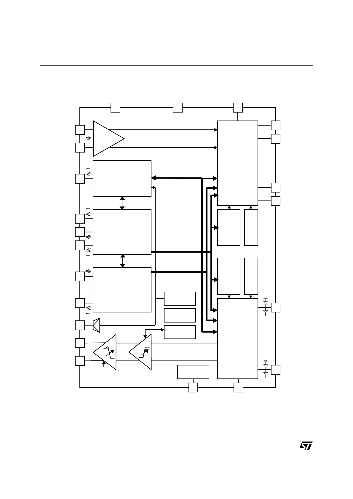
Figure 1. Preampl i f ier bl ock diagram
VCC (+5V) VGND (0V) VDD (+8V)
WDX
WDY
FLT
SDATA
SCLK
SDEN
R/W
MRR
ABHV/
ADT V
RDX
PREDRIVER
3v
FAULT PROCESSOR
Low supp ly detection,
Open/short heads,
TA detection,
low write frequency,
high temperature
3v
SERIAL INTERFACE
CONTROL
3v
HEAD SELECTION
MODE CONTROL
HW0X
HW0Y
WRITE
DRIVERS
HW1X
HW1Y
WRITE
DAC
Imr, Iwr
RW enable
head sel ect
READ
DAC
&
ABHV,
MR meas
Rdamp
Overshoot
low bias
current/voltage
HR0
Temperature
monitoring
TA d etection,
TA correction
MR
READ
INPUT
STAGES
2/4
RDY
Gain
boost
L6326
VREF
RREF/NC HGND
HR 1
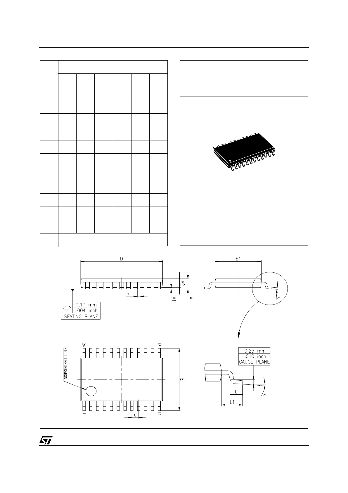
mm inch
DIM.
MIN. TYP. MAX. MIN. TYP. MAX.
A 1.20 0.047
A1 0.05 0.15 0.002 0.006
A2 0.80 1.00 1.05 0.031 0.039 0.041
b 0.19 0.30 0.007 0.012
c 0.09 0.20 0.003 0.008
D 7.70 7.80 7.90 0.303 0.307 0.311
E 6.40 0.252
E1 4.30 4.40 4.50 0.170 0.173 0.177
e 0.65 0.025
L 0.45 0.60 0.75 0.018 0.024 0.030
L6326
OUTLINE AND
MECHANICAL DATA
L1 1.00 0.039
k 0˚ min., 8˚ max.
TSSOP24
Thin Shrink Small Outline Package
7100777 (JEDEC MO-153-AD)
3/4

L6326
Information furnished is believed to be accurate and reliable. However, STMicroelectronics assumes no responsibility for the consequences
of use of such information nor for any infringement of patents or other rights of third parties which may result from its use. No license is granted
by implic ation or o th erwise un der any pat ent or patent right s of STMi croelectr oni cs. Specifications menti oned in th i s publication are s ubj ect
to change without notice. This publication supersedes and replaces all information previously supplied. STMicroelectronics products are not
authorized for use as c ritical components in li fe support devices or syst em s without express wri t ten approval of STMic roelectronics.
The ST logo is a registered trademark of STMicroelectronics
2001 STMi croelectronics - All Ri ghts Reserved
Australi a - Brazil - China - Finland - Fr ance - Germany - Hong Kong - India - Italy - Japan - Malaysia - Malta - Morocco - Singapore - Spain
STMicroelectronics GROUP OF COMPANIES
- Sweden - Sw itzerland - United Kingdom - U. S.A.
http://www.s t. com
4/4
 Loading...