

SGS Thomson Microelectronics L584 Datasheet
MULTIFUNCTIONINJECTION INTERFACE
.DRIVES ONE OR TWO EXTERNAL DAR-
LINGTONS
.DUAL AND SINGLE LEVEL CURRENT CON-
TROL
.SWITCHMODECURRENTREGULATION
.ADJUSTABLEHIGHLEVELCURRENT DURA-
TION
.WIDE SUPPLYRANGE(4.75 - 46V)
.TTL-COMPATIBLELOGICINPUTS
.THERMAL PROTECTION
.DUMP PROTECTION
DESCRIP TIO N
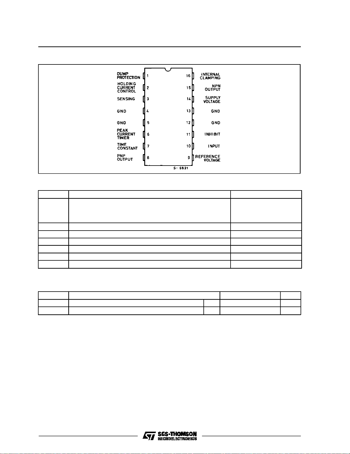
TheL584 is designedto drive injectorsolenoidsin
electronic fuel injection systems and generally inductiveloads for automotive applications.The device is controlled by two logic inputs and features
switchmoderegulationoftheloadcurrentdrivingan
externaldarlingtonandan auxiliaryonefor the current recirculation.A key featureof the L584is flexibility. It canbe used with a varietyof darlingtonsto
match the requirements of the load and it allows
bothsimpleandtwolevelcurrentcontrol.Moreover,
L584
PRELI MINA RY DATA
DIP16 (12+2+2)
ORDERING NUMBER : L584
the drive waveshape can be adjusted by external
components.Other features of the device include
dump protection,thermal shutdown, a supply voltagerangeof4.75-46VandTTL-compatibleinputs.
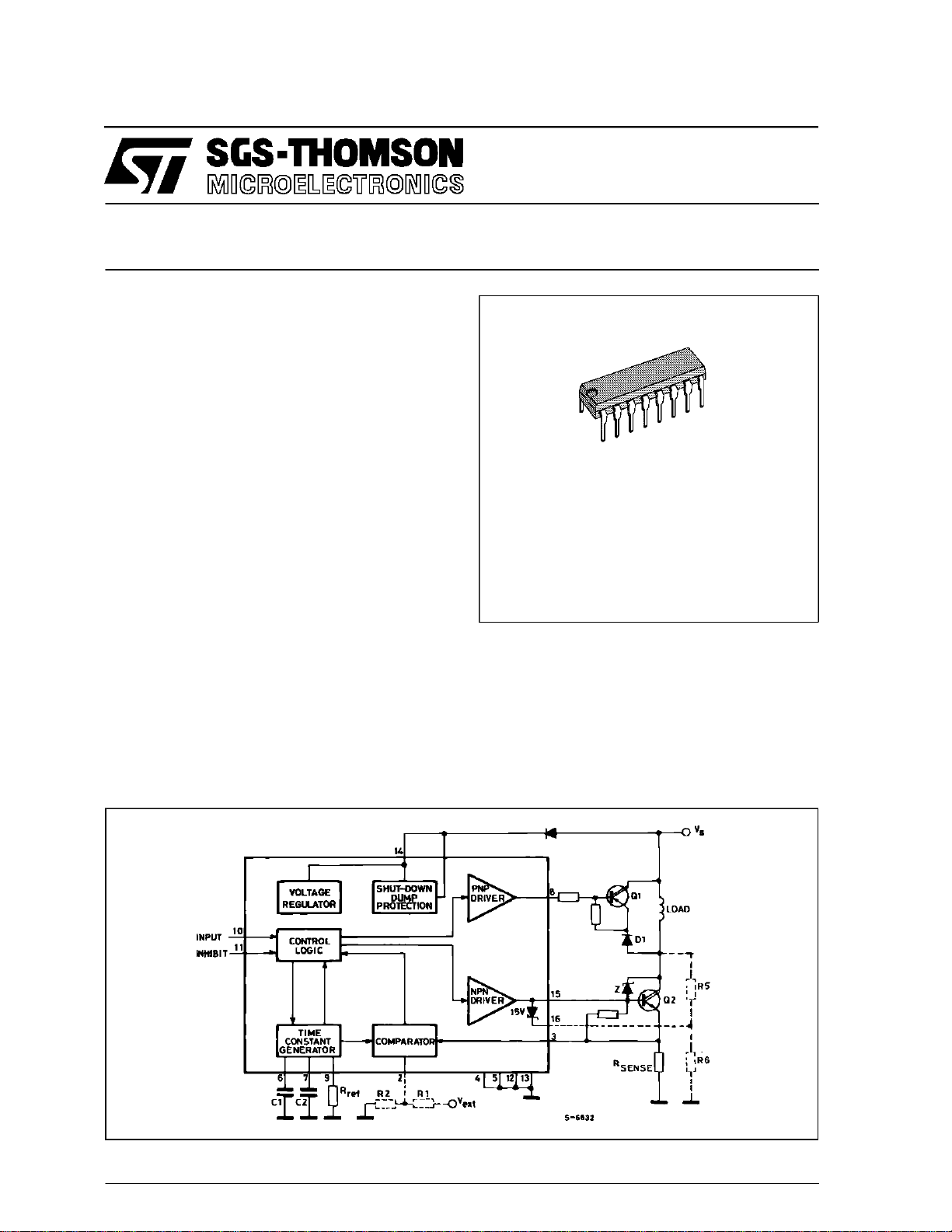
TheL584is suppliedin a16leadPowerdippackage
whichuses the four center pins to conduct heat to
the PC board copper.
BLOCK DIAG RAM
November 1988
1/13
L584
PIN CO NNEC TIO N
ABSOLUTE MAXIMUMRATINGS
Symbol Parameter Value
V
V
V
V
sens
V
I
Tstg,Tj Storageand Junction Temperature Range –55 to 150°C
DC Supply Voltage (pin 1 open)
S
– 0.2Vmin; +50V Max
PositiveTransient Voltage
(pin 1 connected to V
(5ms ≤ t
Input Voltage(pins 10, 11) – 0.2V min;+7V Max
1
ExternalReference Voltage (pin 2) – 0.2V min;+7V Max
r
≤ 10ms,R
rise
, πffalltime constant = 100ms)
S
≥ 0.5Ω)
source
SenseVoltage (pin 3) – 0.2V min;+7V Max
Max D.C. and Transient Voltage 50V
8
ReferenceCurrent (pin 9) 5mA Max
r
+60VMax
THERMAL DATA
Symbol Parameter Value Unit
R
th j-pins
R
th j-amb
* Obtained with the GND pins soldered to printed circuitwith minimized copper area.
2/13
ThermalResistance Junction-pins Max. 15 °C/W
ThermalResistance Junction-ambient Max. 80 °C/W
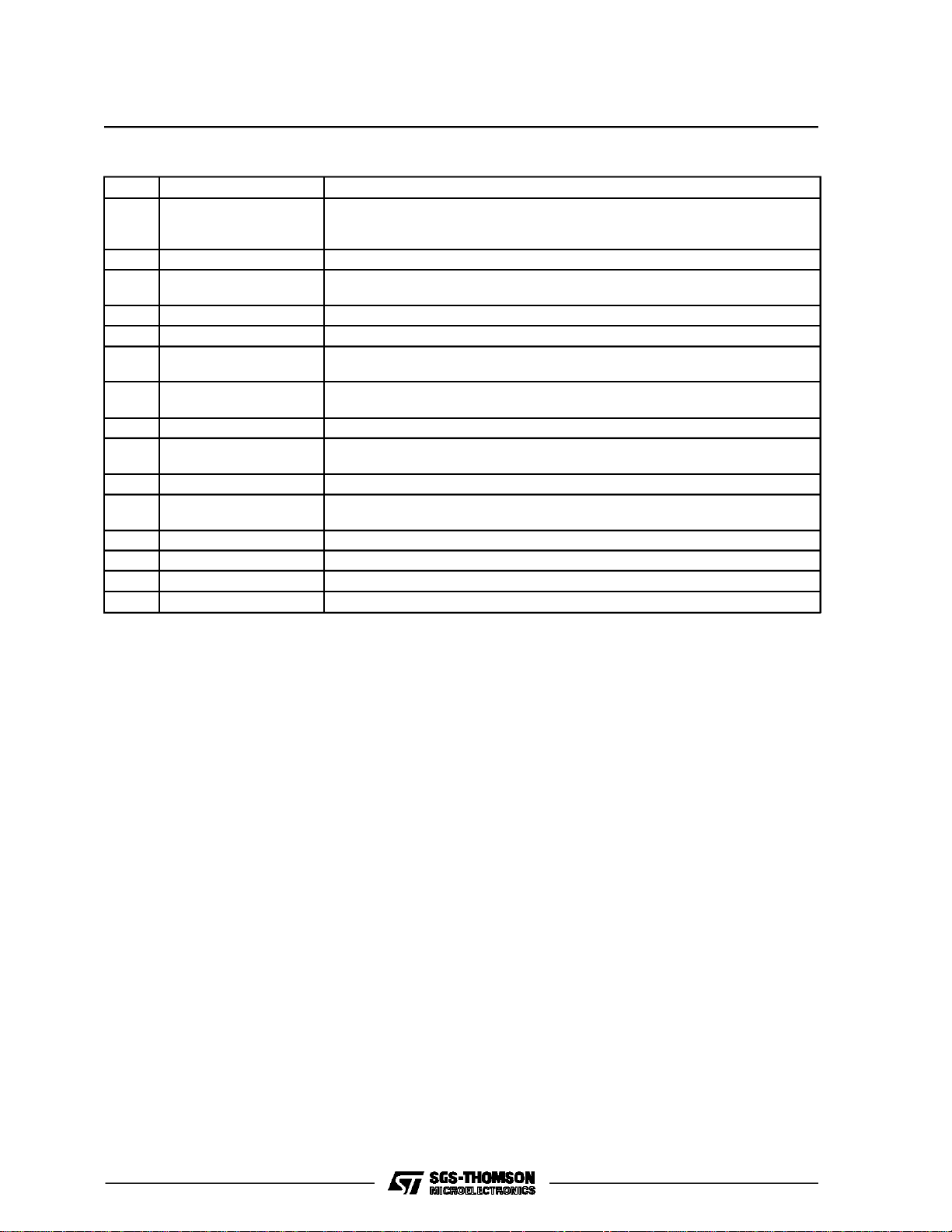
PIN FUNCTIONS
o
N
Name Functions
1 Dump Protection With pin 1 connected to pin 14 the device is protectedagainst dump voltage ≤ 60V.
Theprotectio.n operates at V
≥ 32V(typ.).If this protectionis notused thepin must
S
beleft open
2 HoldingCurrent Control Thevoltage V
appliedto this pin sets the holding current level.
set
3 Sensing Connection for load current sense resistor. Vazlue sets thepeak and holding current
levels. I
=0.45/RS(typ.);Ih=V
P
. (see block diagram and fig. 4).
set/Rs
4 Ground Ground Connection. With pins 5, 12 and13 conducts heat to pc board copper.
5 Ground See pin 4.
6 PeakCurrent Timer A capacitorconnected between this pin andgroundsets the duration of the high level
current(t
7 Discharge Time Constant A capacitor connected between this pin and ground sets the duration of t
infig. 4)
2
off
grounded, the current switchmode control is suppressed.
8 PNP DrivingOutput Current sink for external PNPdarlington (for recirculation). I
= 35 Ir (typ).
dp
9 ReferenceVoltage A resistorconnected between this pin and ground setsthe internal current reference,
I
. The recommended value is 1.2kΩ givingIr = 1mA (typ.).
r
10 Input TTL-compatible Input. A highlevel on this pin activatesthe output, drivingthe load.
11 Inhibit TTL-compatible Inhibit Input.A high level on this input disablesthe output stagesand
logic circutry, irrespectiveof the state of pin 10.
12,13 Ground See Pin 4.
14 Supply Voltage Supply Voltage Input.
15 NPN Driving Output Current Source for ExternalNPN Darlington (load driver).I
=100 Ir(typ.)
dn
16 Internal Clamping Internal Clamp Zener for Fast Turn-off.
000
L584
(fig.4). If
3/13
L584
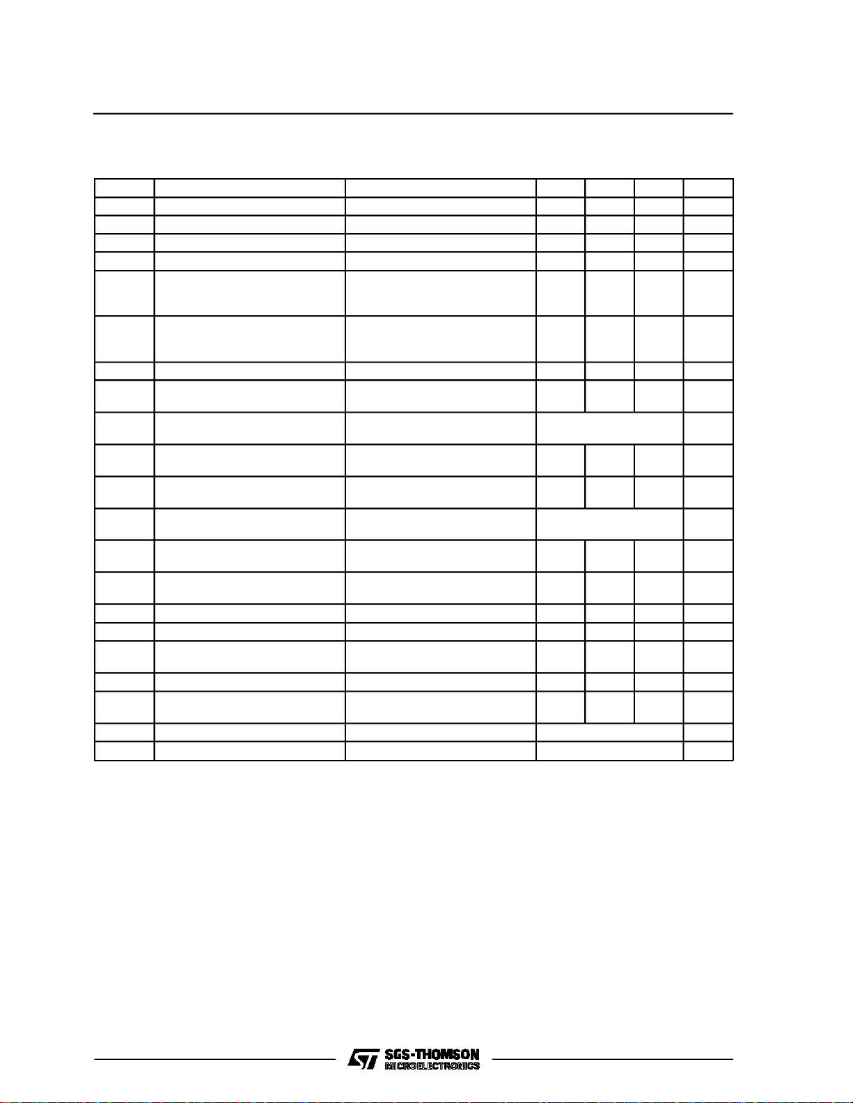
ELECTRICAL CHARACTERISTICS (Vs(Pin 14) = 14.4V; –40 ≤ Tj ≤ 105°C; R
= 1.20KΩ unless
ref
otherwise specified; refer to fig. 1)
Symbol Parameter Test Condiction Min. Typ. Max. Unit
OperatingSupply Voltage Pin1 Open 4.75 44 V
V
S
V
V
V
R
I
V
I
V
R
I
V
6SAT
I
V
7SAT
V
V
V
I
V
I
dn
I
dp
Dump ProtectionThreshold Pin 1 = V
d
Dump ProtectionInput Resistance Pin 1 to GND 18 50 kΩ
d
QuiescentCurrent Pin 14 45 mA
q
Input Threshold Voltages Pin10, 11
i
S
Low
High 2.0
Input Current Pin 10, 11
i
Low
High
ReferenceVoltage Pin 9 1.15 1.35 V
r
ReferenceResistor Range Pin 9 to GND
r
PeakDuration ControlCurrent Pin 6
6
PeakDuration Control
6th
I
r=Vr/Rr
V
≤ 1.8V
pin6
Pin 6 1.20 1.6 V
Comparator Threshold
Pin6 SaturationVoltage Pin 6
(dischargestate)
Off DurationControl Current Pin 7
7
Off DurationControl
7th
V
≤ 1.8V
pin7
Pin 7 1.20 1.6 V
Comparator Threshold
Pin7 SaturationVoltage Pin 7
(dischargestate)
PeakCurrent Threshold Voltage Pin 3 400 500 mV
spt
Holding Current SetVoltage Range Pin 2 0 2 V
set
Holding Current SetVoltage Range Pin 3, Peak Value, dV/dt ≤ 1V/
set
Pin3 Bias Current V
3
Recirculation Zener Clamping
cl
= 600mV –200 µA
pin3
Pin16to Pin15@200mAintoPin16 13.5 18.5 V
s
Voltage
NPN Driver Source Current V
=0V 70xIr| 140 x I
pin15
PNP Driver Sink Current Vpin 8 ≥ 4.75V 25 x Ir|60xI
28 36 V
0.8 V
–100
–250
1 3.3 kΩ
/9.50 | Ir/6.00
I
r
|
200 mV
(I
r min
)/9.50 | (I
r max
)/6.00
|
200 mV
V
set
0.01
–
V
set
0.01
+
r
r
V
µA
µA
A
A
V
A
A
4/13
 Loading...