

OCTAL LINE DRIVERFOR:
– EIASTD: RS232D;RS423A
– CCIT:V.10; V.28
NO EXTERNALCOMPONENTS
VERYLONG TRANSMISSIONLINE (5000ft)
50V EOS OUTPUTPROTECTION
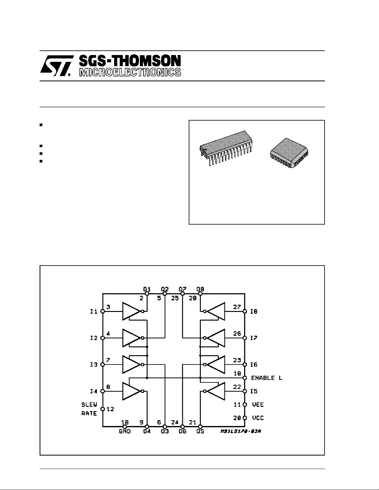
DESCRIPTION
L5170 is an octal line driver unit in DIP28 and
PLCC28 packages intended for use in the EIA std
RS232D, RS423A and CCITT V.10 and V.28 applications.
With no external components L5170 is able to
drive a line up to 5000ft assuming the line capacitance is 35pFper ft and the capacitanceof the filter connectors/protection components add up to
L5170
OCTAL LINE DRIVER
ADVANCE DATA
DIP28 PLCC28
ORDERING NUMBERS:
L5170A L5170D
the total capacitance load. The drivers typically
run in short circuit currentmode whenever thecable attachedis over 500ft.
BLOCK DIAGRAM
March 1993
This isadvanced information on anew productnow in development or undergoing evaluation. Details are subject to change without notice.
1/9
L5170
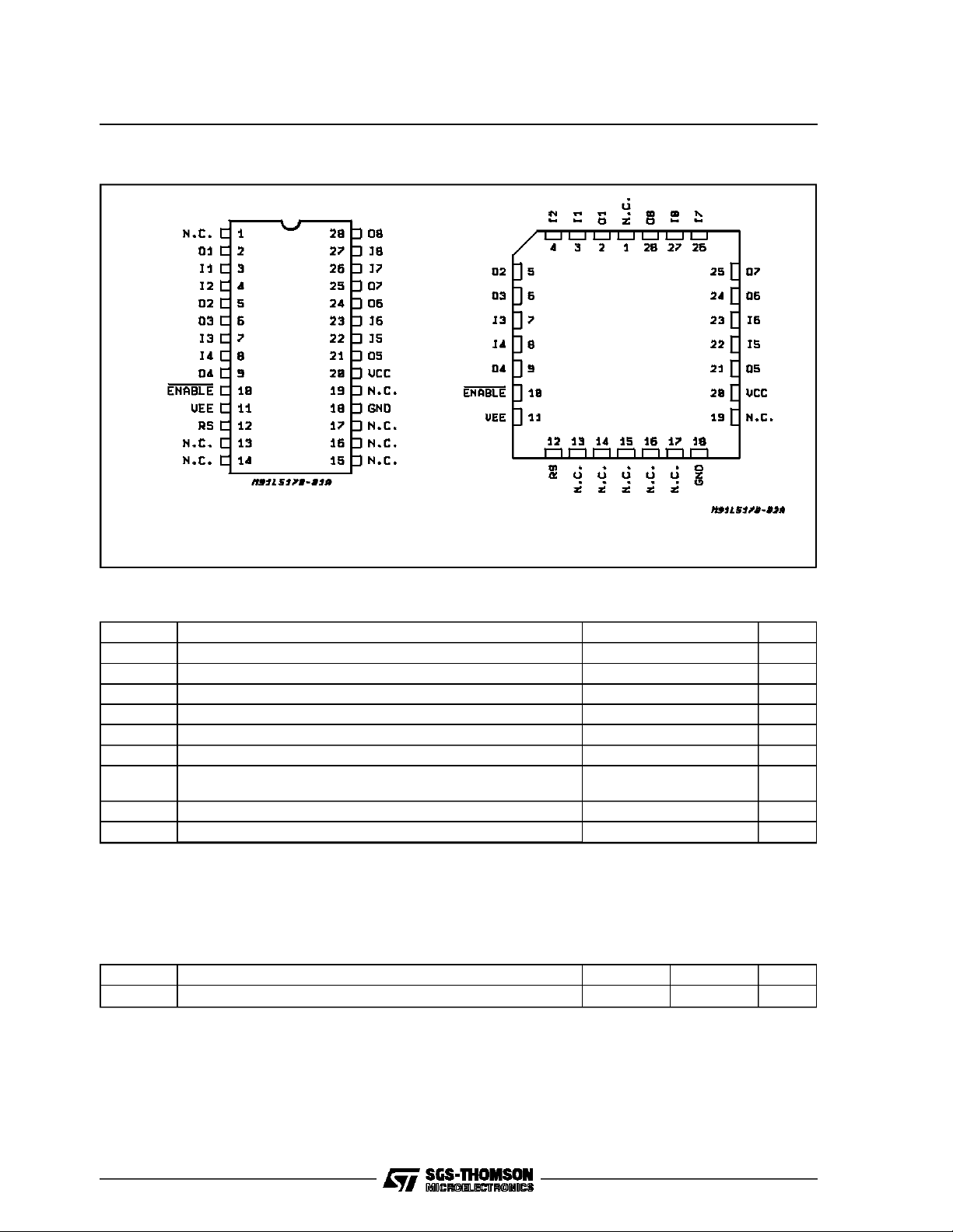
PIN CONNECTIONS (Top views)
DIP28
PLCC28
ABSOLUTE MAXIMUMRATINGS
Symbol Parameter Value Unit
V
CC
V
EE
V
V
O
I
O
Supply Voltage +15 V
Supply Voltage – 15 V
Input Voltage (Enable Data) – 1.5 to 7 V
i
Output Voltage ±6V
Output Current (**) ±150 mA
SR Minimum Slew Resistor (***) 1.5 1KΩ
P
tot
T
op
T
stg
Notes:
(*) Mounted on board with minimized dissipating copper area.
(**) Minimum Current per driver. Do not exceed maximumpower dissipation if more than one input is on.
(***) Minimum value of theresistor used to set the slew rate.
Power Dissipation at T
Operating Free Air Temperature Range 0 to +70 °C
Storage Temperature Range -65 to 150 °C
=70°C(PLCC28) (*)
amb
(DIP28) (*)
1.2
1.3
THERMAL DATA
Symbol Description PLCC28 DIP28 Unit
R
th j-amb
Thermal Resistance Junction-ambient (*) Max. 67 62 °C/W
W
W
2/9
L5170
AC ELECTRICAL CHARACTERISTICS (VCC= 9 to 11V; VEE= – 9 to – 11V T
=0 to 70°C, unless
amb
otherwisespecified
Symbol Parameter Test Condition Min. Typ. Max. Unit
V
OH
V
OL
V
Ol
V
IH
V
IL
V
IK
I
IH
I
IL
I
CC
I
CC1
I
EE
I
EE1
I
sh
I
sl
I
bal
I
x
t
r
t
rc1
t
rc2
t
rc3
t
rc4
t
f
t
fc1
t
fc2
t
fc3
t
fc4
Note 1: The Output under load mustnot drop below 90% of the open circuitdrive level.
Note 2: This represents the static condition only. Applicationscan see 130mA normal current draw for clock and data lines with up to 500mA
transients when all linesaretransitioningat the sametime. Over 500ftof cable slew rate is governedby thedrivers ability to sink current.
The currents are rougly equivalentto the short circuit current.
High Level Output Voltage Vin= 0.8V
R
= inf
L
R
=3KΩ
L
R
= 450Ω (see note 1)
L
5
5
4.5
6
6
6
V
V
V
Low Level Output Voltage Vin= 2.4V
R
= inf
L
R
=3KΩ
L
R
= 450Ω (see note 1)
L
–6
–6
–6
–5
–5
– 4.5
V
V
V
Output Voltage Balance |VCC|=|VEE|; RL= 450Ω 0.4 V
High Level Input Voltage 2 V
Low Level Input Voltage 0.8 V
Input Clamp Voltage IIN= – 15mA –1.5 V
High Level Input Current VIN= 2.4V 40 µA
Low Level Input Current VIN= 0.4V –400 µA
Positive Supply Current VIN=2.4V;RS=2KΩ;RL=3KΩ
C
= 2.5nF; (See note 2)
L
Positive Supply Current VIN=0.4V;RS=2KΩ;RL=3KΩ
C
= 2.5nF; (See note 2)
L
Negative Supply Current VIN=2.4V;RS=2KΩ;RL=3KΩ
C
= 2.5nF; (See note 2)
L
Negative Supply Current VIN=0.4V;RS=2KΩ;RL=3KΩ
C
= 2.5nF; (See note 2)
L
–30 mA
–40 mA
30 mA
40 mA
Output Short Circuit Current VO= 0V; VIN= 2.4V; (see fig.1) 25 100 mA
Output Short Circuit Current VO= 0V; VIN= 2.4V; (see fig.1) – 100 – 25 mA
Output Current Balance Ish/Isl = Ibal 0.625 1.6 mA/mA
Output Leakage Current See fig.2,3 and note 3
V
Rise time (see note 4 and 5; see
figure 4A)
Fall time (see note 4 and 5;see
figure 4A)
=6V
O
V
= – 6V – 70
O
RL= 450Ω;CL= 50pF
R
= 5.34KΩ ±1%
slew
RL= 450Ω;CL= 0.01µF
R
= 10KΩ ±1%
slew
RL= 450Ω;CL= 0.1µF
R
= 10KΩ ±1%
slew
RL= 450Ω;CL= 2.5nF
R
=2KΩ±1%
slew
RL= 450Ω;CL= 2.5nF
R
= 10KΩ ±1%
slew
RL= 450Ω;CL= 50pF
R
= 5.34KΩ ±1%
slew
RL= 450Ω;CL= 0.01µF
R
= 10KΩ ±1%
slew
RL= 450Ω;CL= 0.1µF
R
= 10KΩ ±1%
slew
RL= 450Ω;CL= 2.5nF
R
=2KΩ±1%
slew
RL= 450Ω;CL= 2.5nF
R
= 10KΩ ±1%
slew
2 2.7 µs
0.65 1.2 µs
3.25 6 µs
2 2.7 µs
0.65 1.2 µs
3.25 6 µs
70 µA
µA
10 µs
50 µs
10 µs
50 µs
3/9
 Loading...