

L4987
VERY LOW DROP VOLTAGE REGULATORS
WITH INHIBIT AND DROPOUT CONTROLFLAG
■ VERYLOWDROPOUTVOLTAGE(0.25V
TYP.)
■ DROPOUTCONTROLFLAG
■ VERYLOW QUIESCENTCURRENT
(TYP.90 µA IN OFF MODE,500µAINON
MODE)
■ OUTPUT CURRENT UP TO200 mA
■ LOGIC-CONTROLLEDELECTRONIC
SHUTDOWN
■ OUTPUT VOLTAGESOF 3V,5V 8.7V 12V
■ INTERNAL CURRENTAND THERMAL LIMIT
■ ONLY2.2µF FORSTABILITY
■ AVAILABLEIN ± 2%SELECTIONAT25
■ SUPPLYVOLTAGEREJECTION:70 dB (TYP.)
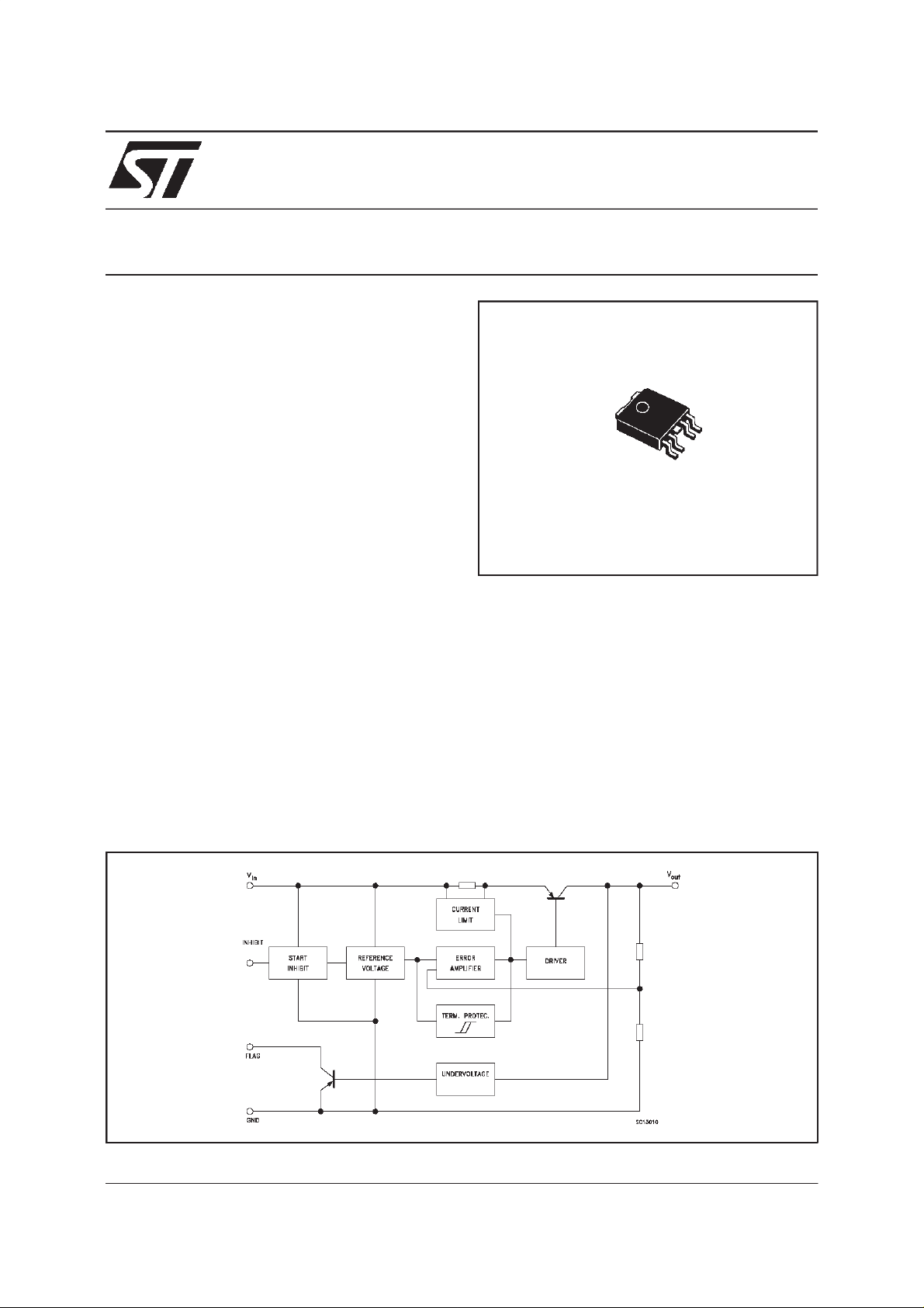
DESCRIPTION
The L4987 is a very low drop regulatoravailable
in PPAK. The very low drop-voltage(0.5V Max at
200 mA) and the very low quiescent currentmake
it particularly suitable for low noise, low power
applications,and in battey powered systems. The
input dump protection up to 40V makes it ideal for
automotive applications. a shutdown Logic
Control function is available (pin2, TTL
compatible). This means that when the device is
used as a local regulator, it is possible to put a
o
C
SERIES
PPAK
part of the boad in standby, decreasing the total
power consumption. The regulator employs an
output pin (open collector) providing a logic signal
when the pass transistor is in saturation at low
input voltage, this signal can be used to prevent
the pop-up phenomenon in the car radio. In
battery powered systems (the cellular phone,
notebook) it is possible to use the flag to monitor
the battery charge status through the dropout of
the regulator.
SCHEMATIC DIAGRAM
October 1998
1/11
L4987 SERIES
ABSOLUTE MAXIMUM RATINGS
Symbol Parameter Value Unit
V
DC Input Voltage 40 V
i
OutputCurrent Internally limited mA
I
o
PowerDissipation Internally limited mW
P
tot
Storage Temperature Range - 40 to 150
T
stg
OperatingJunctionTemperatureRange - 40 to 125
T
op
Absolute Maximum Rating are those values beyond wich damage to the device may occur. Functional operation under these conditions is
not implied.
THERMALDATA
Symbol Parameter DPAK/PPAK Unit
R
thj-cas e
R
thj-amb
Thermal Resistance Junction-case
Thermal Resistance Junction-ambient
8
100
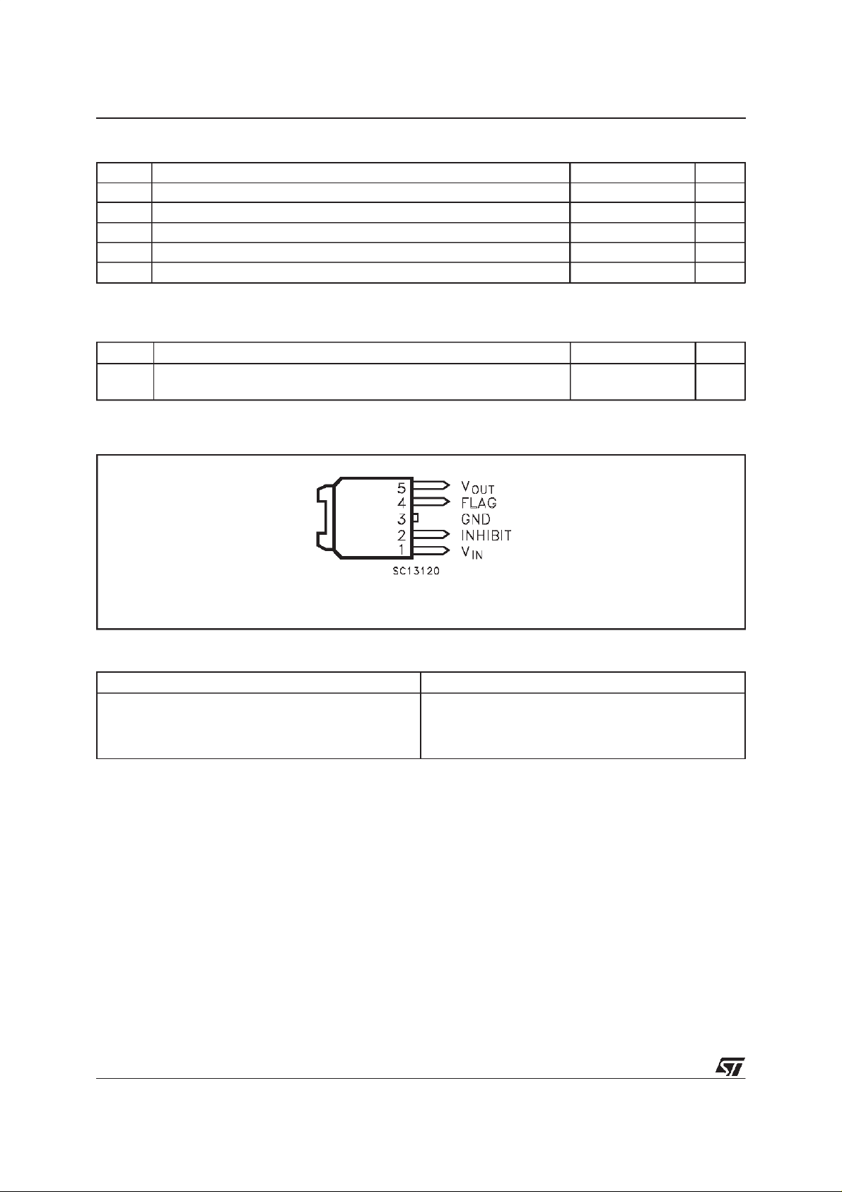
CONNECTION DIAGRAM (top view)
o
o
o
C/W
o
C/W
C
C
ORDERING NUMBERS
L4987CPT30(*)
L4987CPT50(*)
L4987CPT87(*)
L4987CPT120(*)
(*) Available even in tape& reel
2/11
Type Output Voltage
3V
5V
8.7 V
12 V
L4987 SERIES
ELECTRICAL CHARACTERISTICS FOR L4987CPT30
= 5 mA, Tj=25oC, Ci= 0.1 µF, Co= 2.2 µF unless otherwisespecified)
I
OUT
(refer to the test circuits, V
=6V,
I
Symbol Parameter Test Conditions Min. Typ. Max. Unit
OutputVoltage Io=200 mA, Vi=6V
V
I
∆
∆V
o
OperatingInput Voltage Io=200 mA 3.62 18 V
V
i
OutputCurrentLimit 250 A
out
LineRegulation Vi= 4.3to 18 V, Io=0.5mA 2.4 14 mV
V
o
LoadRegulation Vi= 4.1V Io= 0.5to 200 mA 3 20 mV
o
Quiescent Current ON MODE
I
d
=200 mA, Vi= 6 V -40<TJ<125oC
I
o
= 4.3to 18 V Io=0mA
V
i
= 4.3to 18 V Io=200 mA
V
i
OFF MODE V
SVR Supply VoltageRejection
=5 mA Vi=5.3V±1V
I
o
f = 120Hz
f=1KHz
f = 10KHz
Dropout Voltage Io=200 mA
V
d
Control Input Logic Low -40< TJ< 125oC0.8V
V
il
Control Input Logic High -40 < TJ< 125oC2 V
V
ih
Control Input Current 10
I
i
OutputBypassCapacitance
C
O
=200 mA -40< TJ<125oC
I
o
ESR = 0.5 to 10ΩI
-40 < T
Control Flag OutputLow Vi-Vo<V
V
fl
Control Flag OutputHigh
I
fh
I
=200 mA
o
Vi> 3.62V Voh=15V 10 µA
i
< 125oC
J
power, Ifl=6mA
cesat
2.94
2.88
=12V 90 180
= 0 to 200mA
o
210
33.06
3.12
0.7
1.5
1
6
80
75
60
0.25 0.5
0.7
0.5 V
Leakage Current
V
V
mA
mA
A
µ
dB
dB
dB
V
V
A
µ
F
µ
3/11
L4987 SERIES
ELECTRICAL CHARACTERISTICS FOR L4987CPT50
= 5mA, Tj=25oC, Ci= 0.1 µF, Co= 2.2 µF unless otherwise specified)
I
OUT
(refer to the test circuits, V
=8V,
I
Symbol Parameter Test Conditions Min. Typ. Max. Unit
OutputVoltage Io=200 mA, Vi=8V
V
I
∆
∆V
o
OperatingInput Voltage Io=200 mA 5.7 18 V
V
i
OutputCurrentLimit 250 A
out
LineRegulation Vi= 6.3to 18 V, Io=0.5mA 3 20 mV
V
o
LoadRegulation Vi= 3.6V Io= 0.5to 200 mA 3 20 mV
o
Quiescent Current ON MODE
I
d
=200 mA, Vi= 8 V -40<TJ<125oC
I
o
= 6.3to 18 V Io=0mA
V
i
= 6.3to 18 V Io=200 mA
V
i
OFF MODE V
SVR Supply VoltageRejection
=5 mA Vi=7.3V±1V
I
o
f = 120Hz
f=1KHz
f = 10KHz
Dropout Voltage Io=200 mA
V
d
Control Input Logic Low -40< TJ< 125oC0.8V
V
il
Control Input Logic High -40 < TJ< 125oC2 V
V
ih
Control Input Current 10
I
i
OutputBypassCapacitance
C
O
=200 mA -40< TJ<125oC
I
o
ESR = 0.5 to 10ΩI
-40 < T
Control Flag OutputLow Vi-Vo<V
V
fl
Control Flag OutputHigh
I
fh
I
=200 mA
o
Vi> 5.85V Voh=15V 10 µA
i
< 125oC
J
power, Ifl=6mA
cesat
4.9
4.8
=12V 90 180
= 0 to 200mA
o
210
55.1
5.2
0.7
1.5
1
6
76
71
58
0.3 0.5
0.7
0.5 V
Leakage Current
V
V
mA
mA
A
µ
dB
dB
dB
V
V
A
µ
F
µ
4/11
 Loading...