

L4981A
CONTROLBOOSTPWM UP TO0.99P.F.
LIMITLINECURRENT DISTORTIONTO< 5%
UNIVERSALINPUT MAINS
FEED FORWARD LINE AND LOAD REGULA-
TION
AVERAGE CURRENT MODE PWM FOR
MINIMUMNOISE SENSITIVITY
HIGH CURRENT BIPOLAR AND DMOS TO-
TEM POLEOUTPUT
LOW START-UP CURRENT (0.3mATYP.)
UNDER VOLTAGE LOCKOUT WITH HYS-
TERESIS AND PROGRAMMABLE TURN ON
THRESHOLD
OVERVOLTAGE, OVERCURRENT PROTECTION
PRECISE 2% ON CHIP REFERENCE EXTERNALLYAVAILABLE
SOFTSTART
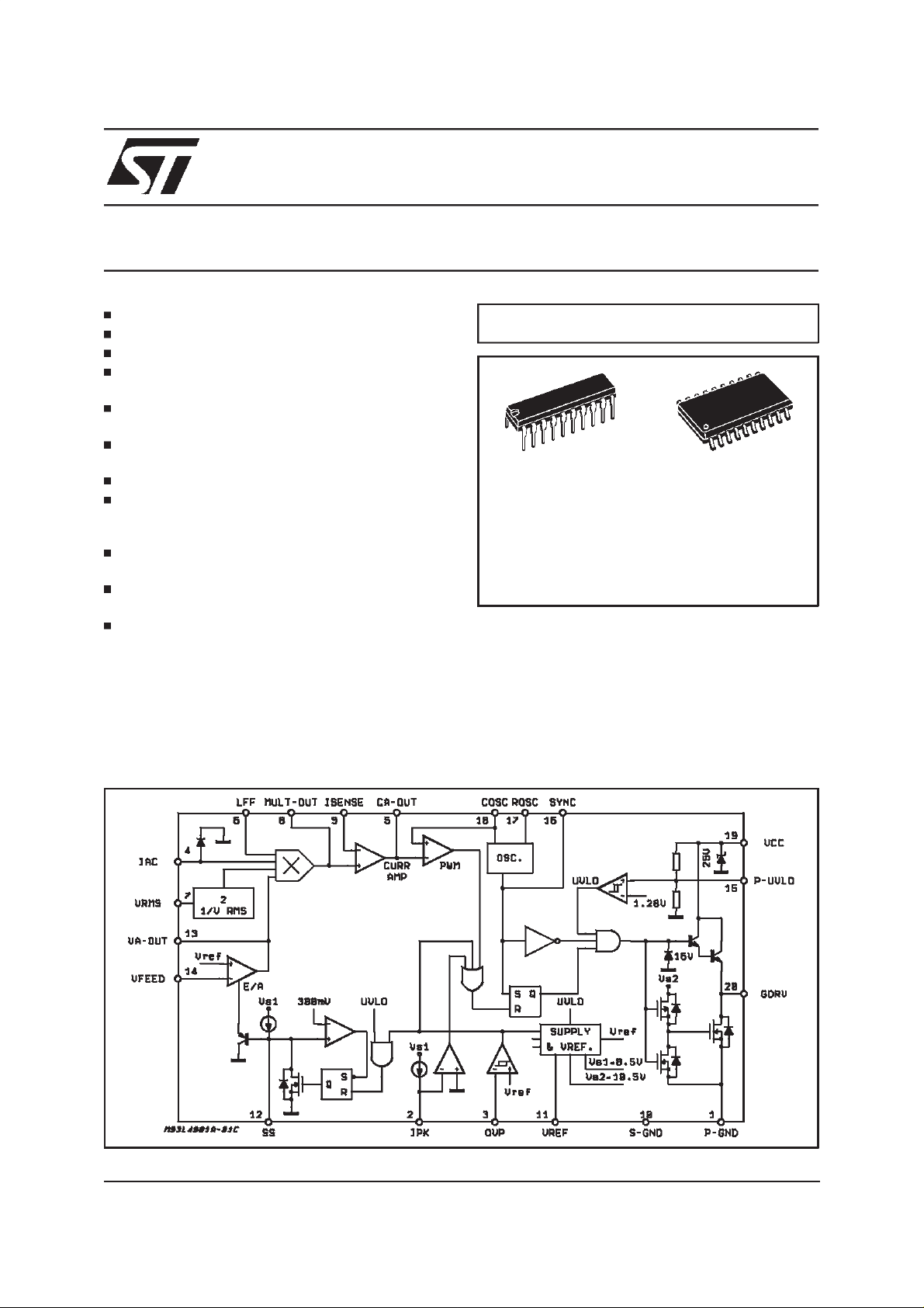
DESCRIPTION
The L4981 I.C. provides the necessary features
to achievea veryhigh power factor up to 0.99.
Realized in BCD 60II technology this power factor
corrector (PFC) pre-regulatorcontains all the con-
L4981B
POWER FACTOR CORRECTOR
MULTIPOWER BCD TECHNOLOGY
DIP20 SO20
ORDERING NUMBERS: L4981X (DIP20)
L4981XD (SO20)
trol functions for designing a highefficiency-mode
power supply with sinusoidal line current consumption.
The L4981 can be easily used in systems with
mains voltages between 85V to 265V without any
line switch. This new PFC offers the possibility to
work at fixed frequency (L4981A) or modulated
frequency (L4981B) optimizing the size of the in-
BLOCK DIAGRAM
September 1998
1/17
L4981A - L4981B
put filter; both the operating frequency modes
working with an averagecurrent mode PWM controller, maintaining sinusoidal line current without
slope compensation.
Besides power MOSFET gate driver, precise voltage reference (externally available), error ampli-
soft start are included. To limit the number of the
external components, the device integrates protections as overvoltage and overcurrent. The
overcurrent level can be programmed using a
simple resistor for L4981A. For a better precision
and for L4981B an external divider must be used.
fier, undervoltage lockout, current sense and the
ABSOLUTE MAXIMUM RATINGS
Symbol Pin Parameter Value Unit
V
I
GDRV
CC
19 Supply Voltage (I
20 Gate driv. output peak current (t = 1µs) SINK 2
. SOURCE 1.5 A
V
GDRV
Gate driv. output voltage t = 0.1µs-1V
Voltages at pins 3, 14, 7, 6, 12, 15 -0.3 to 9 V
V
VA-OUT
AC 4 AC Input Current 5 mA
I
13 Error AmplifierVoltage -0.3 to 8.5 V
Voltages at pin 8, 9 -0.5 to 7 V
CA-OUT 5 Current Amplifier Volt. (Isource = -20mA; Isink = 20mA) -0.3 to 8.5 V
V
V
ROSC
17 Voltage at pin 17 -0.3 to 3 V
11, 18 Voltage at pin 11, 18 -0.3 to 7 V
I
COSC
I
FREQ-MOD
V
SYNC
V
IPK
18 Input Sink Current 15 mA
16 Frequency Modulation Sink Current (L4981B) 5 mA
16 Sync. Voltage (L4981A) -0.3 to 7 V
2 Voltage at pin 2
Voltage at Pin 2 t = 1µs
P
tot Power Dissipation at T
Power Dissipation at T
T
op
T
stg
(*) Maximum package power dissipation limits must be observed.
Operating Ambient Temperature -40 to 125 °C
StorageTemperature -55 to 150 °C
50mA) (*) selflimit V
CC ≤
-0.3 to 5.5
-2
=70°C (DIP20) 1 W
amb
=70°C (SO20) 0.6 W
amb
Α
V
V
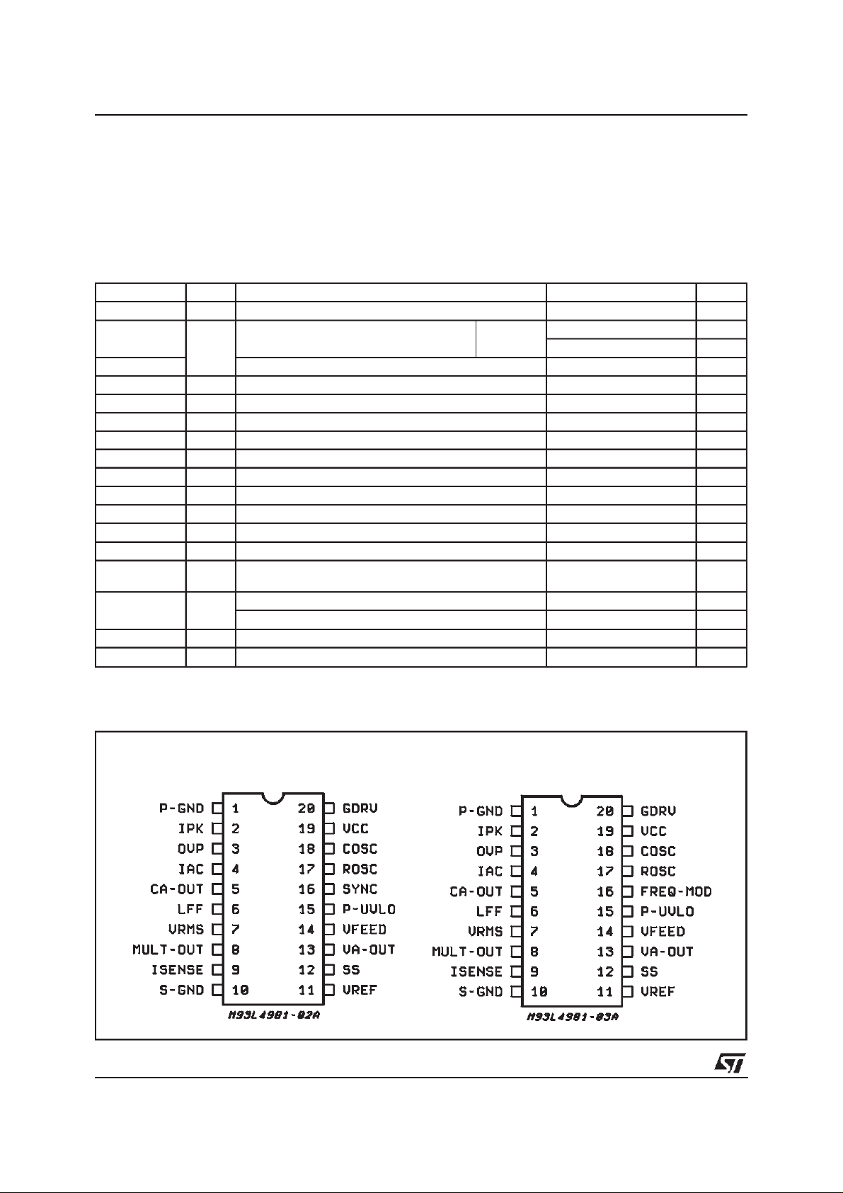
PIN CONNECTIONS (Top views)
L4981A
2/17
L4981B
L4981A - L4981B
THERMAL DATA
Symbol Parameter DIP 20 SO 20 Unit
R
th j-amb
PIN FUNCTIONS
N. Name Description
1 P-GND Power ground.
2 IPK L4981A peak current limiting. A current limitation is obtained using a singleresistor connected
Thermal Resistance Junction-ambient 80 120
between Pin 2 and thesense resistor. To have a better precision another resistor between Pin
2 and a reference voltage (Pin 11) must be added.
C/W
°
L4981B
peak current limiting. A precise current limitation is obtained using two external
resistor only. These resistorsmust be connected between the sense resistor, Pin 2 and the
reference voltage.
3 OVP Overvoltage protection. At this input are compared an internal precise 5.1V (typ) voltage
reference with a sample of the boost output voltage obtained via a resistive voltage divider in
order to limit the maximum output peak voltage.
4 IAC Input for the AC current. An input current proportional to the rectifiedmains voltagegenerates,
via a multiplier,the current reference for the currentamplifier.
5 CA-OUT Current amplifieroutput. An external RC network determinatesthe loop gain.
6 LFF Load feedforward; this voltage input pin allowsto modify the multiplier output current
proportionally to the load, in order to give a faster response versus load transient. The best
control is obtained working between 1.5V and 5.3V. If this function is not used, connect this pin
to the voltagereference (pin = 11).
7 VRMS Input for proportional RMS line voltage. theVRMS input compesates theline voltage changes.
Connecting a low pass filter between therectified line andthe pin 7, a DC voltage proportional
to the inputline RMS voltage is obtained. The best control isreached using input voltage
between 1.5V and 5.5V. Ifthisfunction is not used connectthis pin to the voltage reference
(pin = 11).
8 MULT-OUT Multiplier output. This pin common to the multiplier output and the current amplifier N.I. inputis
9I
SENSE
an high impedence input like I
Current amplifierinverting input. Care must be takento avoid this pin goes down -0.5V.
. The MULT-OUT pin must be taken not below -0.5V.
SENSE
10 S-GND Signal ground.
11 V
REF
Output reference voltage (typ = 5.1V).Voltage refence at ± 2% of accuracy externally available,
it’s internallycurrent limitedand candeliver an output current up to 10mA.
12 SS A capacitor connected to ground defines the soft start time. An internal current generator
delivering 100µA (typ) charges the external capacitor defining the soft start time constant. An
internal MOS discharge,the external soft start capacitor both in overvoltage and UVLO
conditions.
13 VA-OUT Error amplifier output, an RC network fixes the voltage loop gain characteristics.
14 VFEED Voltage error amplifier inverting input. This feedback input is connected via a voltage divider to
the boost outputvoltage.
15 P-UVLO Programmable under voltage lock out threshold input. A voltage divider between supply
voltage and GND can be connected in orderto program the turn on threshold.
16 SYNC
(L4981A)
This synchronization input/output pin is CMOS logic compatible. Operating as SYNC in, a
rectangular wave must be applied at this pin. Opearting as SYNC out,a rectangular clock
pulse train is available to synchronize otherdevices.
FREQ-MOD
(L4981B)
17 R
18 C
19 V
OSC
OSC
CC
Frequency modulation current input. An external resistor must be connected between pin 16
and the rectified line voltage in order to modulate the oscillatorfrequency. Connecting pin 16 to
ground a fixed frequencyimposed by R
An external resistor connected to ground fixes the constant charging current of C
OSC
and C
is obtained.
OSC
OSC
.
An external capacitor connected to GND fixes the switching frequency.
Supply input voltage.
20 GDRV Output gate driver. Bipolar and DMOS transistors totem pole output stage candeliver peak
current in excess1A useful to drive MOSFET or IGBT power stages.
3/17
L4981A - L4981B
ELECTRICALCHARACTERISTICS
R
=24KΩ,CSS=1µF, V
V
OSC
FEED
= GND, V
IPK
= 1V,V
CA-OUT
= 1V, TJ=25°C
OVP
(Unlessotherwise specified V
= 3.5V, V
ISENSE
= 0V, V
LFF=VREF,IAC
= 18V, C
CC
= 1nF,
OSC
= 100µA, V
RMS
= 1V,
Symbol Prameter Test Condition Min. Typ. Max. Unit
ERROR AMPLIFIER SECTION
V
IO
I
IB
Input Offset Voltage –25°C<TJ<85°C ±8mV
Input Bias Current V
= 0V -500 -50 500 nA
FEED
Open Loop Gain 70 100 dB
V
13H
V
13L
-I
13
I
13
Output High voltage V
Output Low Voltage V
Output Source Current V
Output Sink Current V
FEED
I
VA-OUT
FEED
I
VA-OUT
FEED
FEED
= 4.7V
= -0.5mA
= 5.5V
= 0.5mA
= 4.7V; V
= 5.5V; V
5.5 6.5 7.5 V
0.4 1 V
= 3.5V 2 10 mA
VA-OUT
= 3.5V 4 20 mA
VA-OUT
REFERENCE SECTION
V
ref
∆V
ref
∆V
ref
I
ref sc
Reference OutputVoltage –25°C<TJ<85°C 4.97 5.1 5.23 V
=25°CI
T
j
Load Regulation 1mA ≤ I
–25°C<T
Line Regulation 12V ≤ VCC≤ 19V
–25°C<T
Short Circuit Current V
=0V 203050mA
ref
= 0 5.01 5.1 5.19 V
ref
ref
J
≤ 10mA
<85°C
315mV
310mV
<85°C
J
OSCILLATOR SECTION
f
V
I
I
V
osc
svp
18C
18D
18
Initial Accuracy Tj=25°C 85 100 115 KHz
Frequency Stability 12V ≤ V
–25°C<T
CC
J
≤ 19V
<85°C
80 100 120 KHz
Ramp Valley to Peak 4.7 5 5.3 V
Charge Current V
Discharge Current V
= 3.5V 0.45 0.55 0.65 mA
COSC
= 3.5V 11.5 mA
COSC
Ramp Valley Voltage 0.9 1.15 1.4 V
SYNC SECTION (Only for L4981A)
t
W
I
16
-I
16
V
16L
V
16H
t
d
FREQUENCY MODULATION FUNCTION
f
18max
f
18min
Output Pulse Width 50%Amplitude 0.3 0.8 µs
Sink Current with Low Output
Voltage
Source Current with High Output
Voltage
V
V
V
V
SYNC
COSC
SYNC
COSC
= 0.4V
=0V
= 4.5V
= 6.7V
0.4 0.8 mA
16 mA
Low Input Voltage 0.9 V
High Input Voltage 3.5 V
Pulse for Synchronization 800 ns
(Only for
Maximum Oscillation Frequency V
Minimum Oscillator Frequency I
L4981B
FREQ-MOD
FREQ-MOD
V
VRMS
I
FREQ-MOD
V
VRMS
)
= 0V (Pin 16) I
= 360µA (Pin16)
= 4V (Pin 7)
= 180µA (Pin16)
= 2V (Pin 7)
= 0 85 100 115 KHz
freq
74 KHz
76 KHz
SOFT START SECTION
Soft Start SourceCurrent VSS= 3V 60 100 140 µA
Output Saturation Voltage V3= 6V, ISS= 2mA 0.1 0.25 V
V
I
SS
12sat
4/17
L4981A - L4981B
ELECTRICALCHARACTERISTICS
(continued)
Symbol Parameter Test Condition Min. Typ. Max. Unit
SUPPLY VOLTAGE
V
CC
Operating Supply Voltage 19.5 V
OVER VOLTAGE PROTECTION COMPARATOR
Rising Threshold Voltage V
-20mV
ref
5.1 V
+20mV
ref
Hysteresis 180 250 320 mV
Input Bias Current 0.05 1
Propagation delay tooutput V
OVP=Vthr
+100mV 1 2
V
V
3Hys
I
t
thr
3
d
OVER CURRENT PROTECTIONCOMPARATOR
V
th
t
d
I
ipk
I
L
Threshold Voltage ±30 mV
Propagation delay toOutput V
Current Source Generator V
Leakage Current V
OCP=Vthr
IPK
IPK
-0.2V 0.4 0.9 µs
= -0.1V
= -0.1V
only for L4981A
only for L4981B
65 85 105 µA
5 µA
CURRENT AMPLIFIER SECTION
V
offset
I
9bias
Input Offset Voltage V
Input Bias Current V
MULT OUT=VSENSE
SENSE
Open Loop Gain 1.1V≤V
SVR Supply Voltage Rejection 12V ≤ V
V
MULT OUT
V
5H
V
5L
-I
5
I
5
Output High Voltage V
Output Low Voltage V
Output Source Current V
Output Sink Current 2 10 mA
MULT OUT
I
CA OUT
MULT OUT
I
CA OUT
MULT OUT
V
IAC
= 0V, V
= 0V -500 50 500 nA
CA OUT
CC
= 3.5V V
= 200mV
= -0.5mA, V
= -200mV
= 0.5mA, V
= 200mV,
= 3.5V ±2mV
6V 70 100 dB
≤
≤ 19V
SENSE
= 3.5V
68 90 dB
6.2 V
=0V
IAC
=0V
IAC
210 mA
= 3.5V
CA-OUT
0.9 V
OUTPUT SECTION
V
V
V
20L
20H
t
r
t
f
GDRV
Output Voltage Low I
Output Voltage High I
Output Voltage Rise Time C
Output Voltage Fall Time C
Voltage Clamp I
= 250mA 0.5 0.8 V
SINK
= 250mA
SOURCE
V
= 15V
CC
= 1nF 50 150 ns
OUT
= 1nF 30 100 ns
OUT
= 0mA 13 16 19 V
SOURCE
11.5 12.5 V
TOTAL STANDBY CURRENT SECTION
I
19start
I
19on
Supply Current before start up VCC= 14V 0.3 0.5 mA
Supply Current after turn on V
IAC
=0V,V
COSC
=0,
812mA
Pin17= Open
I
19
V
CC
Operating Supply Current Pin20 = 1nF 12 16 mA
Zener Voltage (*) 20 25 30 V
UNDER VOLTAGE LOCKOUT SECTION
V
V
th OFF
thON
Turn on Threshold 14.5 15.5 16.5 V
Turn off Threshold 9 10 11 V
Programmable Turn-on Threshold Pin 15 to V
CC
= 220K
10.6 12 13.4 V
Pin15 to GND = 33K
LOAD FEED FORWARD
I
LFF
V
I
(*) Maximum package power dissipation limits must be observed.
Bias Current V6= 1.6V 70 140
= 5.3V 200 300 µA
V
6
Input Voltage Range 1.6 5.3 V
V
A
µ
s
µ
A
µ
5/17
L4981A - L4981B
ELECTRICALCHARACTERISTICS
(continued)
Symbol Prameter Test Condition Min. Typ. Max. Unit
MULTIPLIER SECTION
Multipler Output Current V
V
MULTOUT
I
AC
V
VA-OUT
V
MULTOUT
I
AC
V
VA-OUT
V
MULTOUT
I
AC
V
VA-OUT
V
MULTOUT
I
AC
V
VA-OUT
V
MULTOUT
I
AC
V
VA-OUT
V
MULTOUT
C
OSC
V
VA-OUT
V
MULTOUT
I
AC
V
VA-OUT
V
MULTOUT
I
AC
=0,V
=50µA, COSC =0V
= 4V, V
=0,V
= 200µA, C
= 2V, V
=0,V
= 100µA, C
= 2V, V
=0,V
= 100µA, COSC =0V
= 4V, V
=0,V
= 100µA, C
= 4V, V
=0,V
= 0V, IAC= 200µA
= 4V, V
=0,V
= 200µA, COSC =0V
= 2V, V
=0,V
=0,C
OSC
= 4V, V
VA-OUT
RMS
LFF
RMS
LFF
OSC
RMS
LFF
OSC
RMS
LFF
RMS
LFF
OSC
RMS
LFF
RMS
LFF
RMS
LFF
=0V
= 2V,
= 5.1V
= 2V,
= 5.1V
=0V
= 2V,
= 5.1V
=0V
= 4V,
= 5.1V
= 4V,
= 5.1V
=0V
= 2V,
= 2.5V
=4V
= 5.1V
= 4V,
= 5.1V
20 35 52
100 135 170 µA
10 20 30 µA
2 5.5 11
10 22 34 µA
20 37 54 µA
20 39 54
-2 0 2 µA
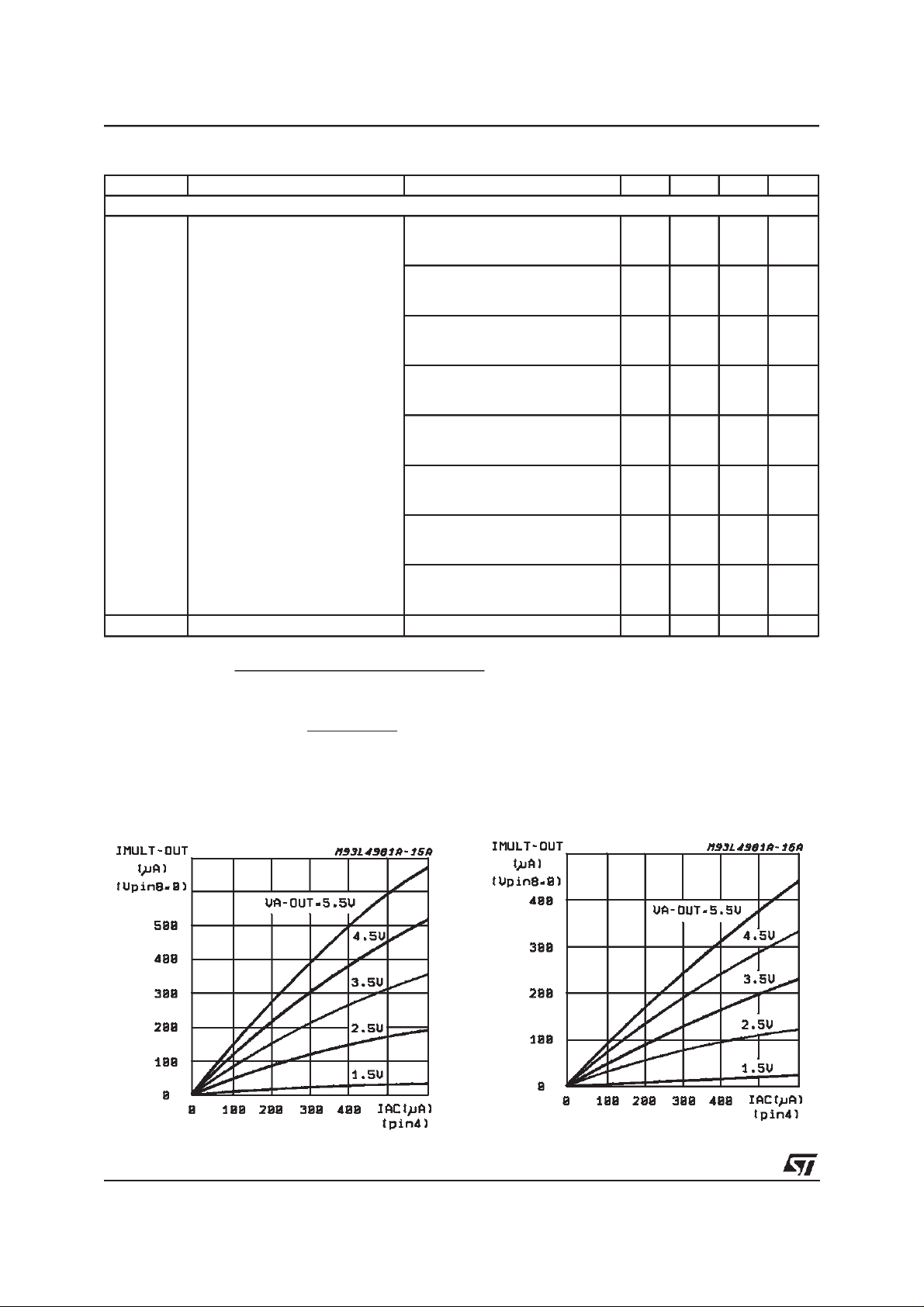
K Multiplier Gain 0.37
A
µ
A
µ
A
µ
I
MULT−OUT
= K ⋅ I
if VLFF =VREF; I
where: K1 = 1V
Figure 1:
MULTI-OUTvs. I
V
LFFD
(
V
AC
MULT−OUT
= 5.1V)
VA−OUT
= I
−
1.28
(V
(V
−OUT
VA
AC
(V
AC(VRMS
) ⋅ (
VRMS
− 1.28)
VRMS
= 1.7V;
0.8⋅V
2
)
2
)
LFF
⋅ K1
−
)
1.28
Figure2: MULTI-OUTvs. I
V
LFFD
= 5.1V)
AC(VRMS
= 2.2V;
6/17
 Loading...