

SGS Thomson Microelectronics L4976D, L4976 Datasheet
1A STEP DOWN SWITCHING REGULATOR
UP TO 1A STEP DOWN CONVERTER
OPERATINGINPUT VOLTAGE FROM 8V TO
55V
PRECISE5.1V REFERENCEVOLTAGE
OUTPUT VOLTAGE ADJUSTABLE FROM
3.3VTO 50V
SWITCHINGFREQUENCY ADJUSTABLE UP
TO 500KHz
VOLTAGEFEEDFORWARD
ZEROLOAD CURRENTOPERATION
INTERNAL CURRENT LIMITING (PULSE-BY-
PULSEAND HICCUPMODE)
PROTECTION AGAINST FEEDBACK DIS-
CONNECTION
THERMAL SHUTDOWN
DESCRIPTION
The L4976 is a step down monolithic power
switching regulator delivering 1A at a voltage between 3.3V and 50V (selected by a simpleexternal divider). Realized in BCD mixed technology,
the device uses an internal power D-MOS transistor (with a typical Rdson of 0.25Ω) to obtain very
high efficency and high switching speed.
A switching frequency up to 250KHz is achievable (themaximum power dissipationof thepack-
L4976
Minidip SO16W
ORDERING NUMBERS: L4976 (Minidip)
L4976D (SO16)
ages must be observed).
A wide input voltage range between 8V to 55V
and output voltages regulated from 3.3V to 40V
cover the majority of today’s applications.
Features of this new generations of DC-DC converter include pulse-by-pulse current limit, hiccup
mode for short circuit protection, voltage feedforward regulation, protection against feedbackloop
disconnectionand thermalshutdown.
The device is available in plastic dual in line,
MINIDIP 8 for standard assembly, and SO16W
for SMD assembly.
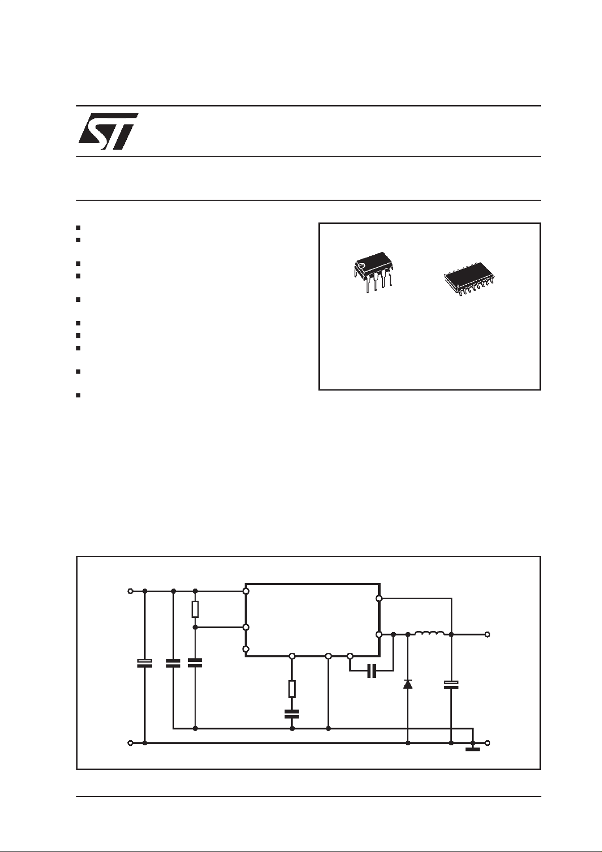
TYPICAL APPLICATIONCIRCUIT
Vi=8V to 55V
R
1
20K
C
2
2.7nF
May 2000
C1
220µ
63V
C
F
7
220nF
5
3
2
L4976
7
R
2
9.1K
22nF
1
C
4
6
C
6
100nF
8
4
L1
260µ
H
(77120)
D1
GI
SB360
C
8
330µF
=3.3V/1A
V
O
1/11
L4976
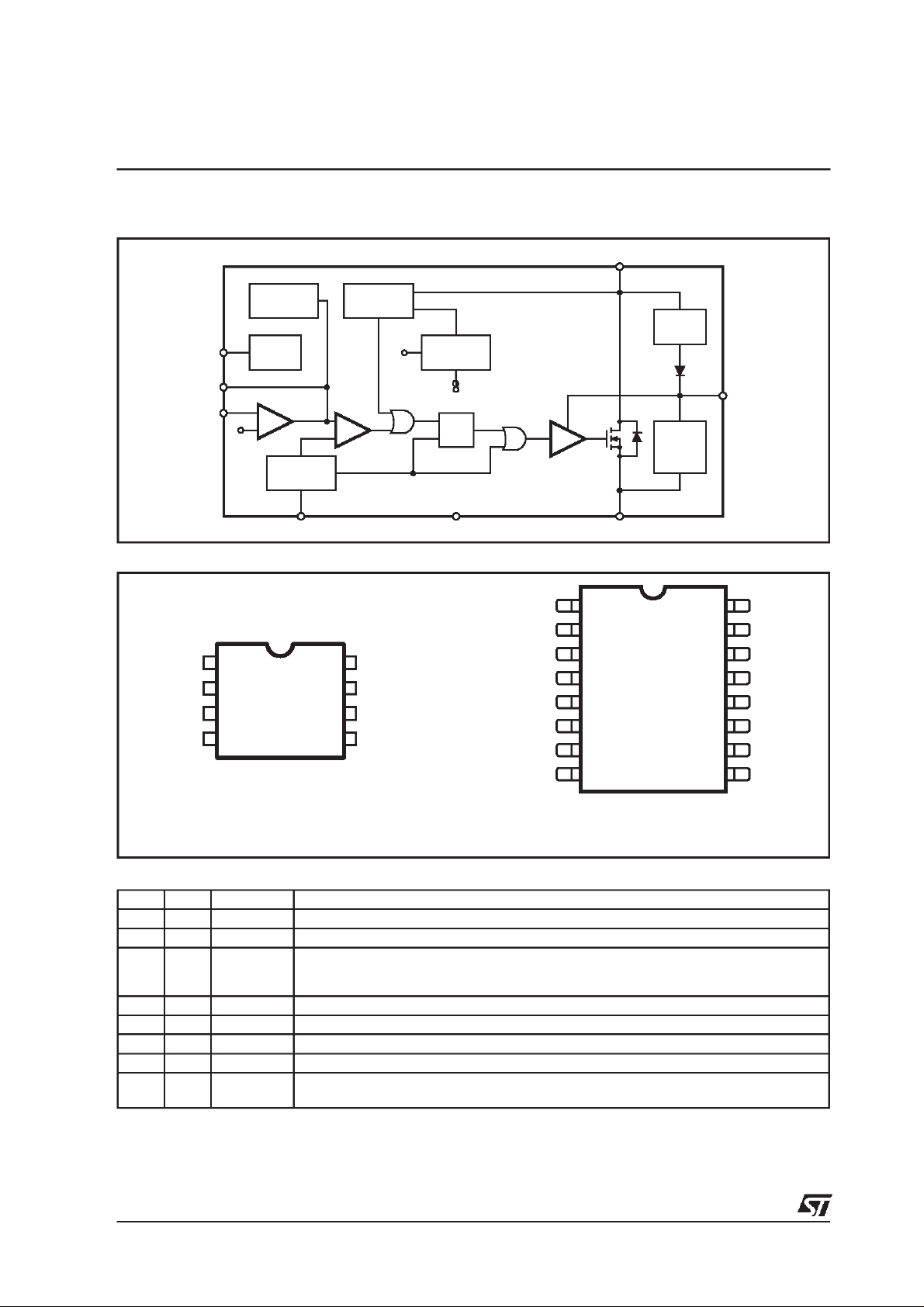
BLOCKDIAGRAM
2
V
REF
7
COMP
8
FB
3.3V
THERMAL
SHUTDOWN
VREF
E/A
OSCILLATOR
VOLTAGES
MONITOR
PWM
5.1V
INTERNAL
REFERENCE
3.3V
R
Q
S
DRIVE
CC
V
5
CBOOT
CHARGE
6
BOOT
CBOOT
CHARGE
AT LIGHT
LOADS
3
OSC GND OUT
1
4
PIN CONNECTIONS
GND
REF
V
OSC
OUT
1
2
3
4 VCC
FB8
COMP
7
BOOT
6
5
Minidip
N.C.
GND
V
REF
OSC
OUT
OUT
N.C.
N.C. N.C.
2
3
4
5
6
7
8
SO16W
16
15
14
13
12
11
10
9
PIN FUNCTIONS
DIP SO (*) Name Function
1 2 GND Ground
2 3 VREF 5.1V Reference voltage with 20mA current capability.
3 4 OSC An external resistor connected between the unregulated input voltage and this pin and
4 5,6 OUT Stepdown regulator output
511 V
CC Unregulated DC input voltage
6 12 BOOT A capacitor connected between this pin and OUT allows to drive the internal VDMOS
7 13 COMP E/A output to be used for frequency compensation
8 14 FB Stepdown feedback input. Connecting directly to this pin results in an output voltage of
(*) Pins 1, 7,8, 9, 10, 15 and 16 are not internally, electrically connected to the die.
a capacitor connected from this pin to ground fix the switching frequency. (Line feed
forward is automatically obtained)
3.3V. An externalresistive divider is required for higher output voltages.
N.C.1
N.C.
FB
COMP
BOOT
VCC
N.C.
2/11
THERMALDATA
Symbol Parameter Minidip SO16 Unit
R
th(j-amb)
(*) Package mounted on board.
Thermal Resistance Junction to ambient Max. 90 (*) 110 (*) °C/W
OPERATINGTEMPERATURE RATING
Symbol Parameter Value Unit
T
Junction Temperature Range -40 to 150 °C
J
ABSOLUTE MAXIMUM RATINGS
L4976
Symbol
Minidip S016
V
11
V5,V
I5,I
V12-V
V
12
V
13
V
14
P
tot
V
V
5
V
4
I
4
6-V5
V
6
V
7
V
8
Input voltage 58 V
Output DC voltage
6
Output peak voltage at t = 0.1µs f=200KHz
Maximum output current int. limit.
6
11
Bootstrap voltage 70 V
Analogs input voltage (VCC= 24V) 12 V
(VCC= 20V) 6
Power dissipation a T
Parameter Value Unit
-1
-5
V
V
14 V
V
-0.3
≤ 60°C Minidip 1W
amb
V
SO16 0.8 W
T
j,Tstg
Junction and storage temperature -40 to 150 °C
ELECTRICAL CHARACTERISTICS (Tj = 25°C, Cosc = 2.7nF, Rosc = 20kΩ,VCC = 24V, unless other-
wisespecified.) * SpecificationRefered to Tj from 0 to 125°C
Symbol Parameter Test Condition Min. Typ. Max. Unit
DYNAMICCHARACTERISTIC
V
V
o Output voltage Io = 0.5A 3.33 3.36 3.39 V
V
d Dropout voltage Vcc = 10V;Io = 1A 0.44 0.55 V
I
l Maximum limiting current Vcc = 8 to 55V * 1.5 2 2.5 A
f
s Switching frequency * 90 100 110 KHz
SVRR Supply voltage ripple rejection V
Operating input voltage range Vo= 3.3 to 50V; Io=1A * 8 55 V
I
I
o = 0.2 to 1A 3.292 3.36 3.427 V
V
cc = 8to 55V * 3.22 3.36 3.5 V
* 0.88 V
Efficiency V
Voltage stability of switching
o = 3.3V; Io =1A 85 %
+2V
i=Vcc
I
o = 1.A; f ripple = 100Hz
RMS;Vo=Vref
;
60 dB
Vcc = 8 to 55V 3 6 %
frequency
Temp. stability of switching
T
j = 0 to 125°C4%
frequency
3/11
L4976
ELECTRICAL CHARACTERISTICS (continued)
Symbol Parameter Test Condition Min. Typ. Max. Unit
Reference Section
Reference Voltage 5.0 5.1 5.2 V
I
= 0 to 10mA;
ref
V
= 8 to 55V
CC
Line Regulation I
Load Regulation V
= 0mA;
ref
V
= 8 to 55V
CC
= 0 to 5mA;
ref
V
= 0 to 20mA
CC
Short Circuit Current 30 65 100 mA
DC Characteristics
Iqop Total operating quiescent
I
q Quiescent current Duty Cycle = 0; V
current
= 3.8V 2.5 3.5 mA
FB
Error Amplifier
V
FB
R
L
V
oH High level output voltage V
V
oL Low level output voltage V
I
o source Source output current V
I
o sink Sink output current V
I
b Source bias current 2 3 µA
SVRR E/A Supply voltage ripple rejection V
gm Transconductance I
Voltage Feedback Input 3.33 3.36 3.39 V
Line regulation Vcc= 8 to 55V 5 10 mV
Ref. voltage stability vs
temperature
= 2.5V 10.3 V
FB
= 3.8V 0.65 V
FB
= 6V; VFB= 2.5V 180 220 µA
comp
= 6V; VFB= 3.8V 200 300 µA
comp
; Vcc = 8 to 55V 60 80 dB
= ∞ 50 57 dB
= -0.1 to 0.1mA
=6V
DC open loop gain R
comp=Vfb
L
comp
V
comp
OscillatorSection
Ramp Valley 0.78 0.85 0.92 V
Ramp peak Vcc= 8V 2 2.15 2.3 V
Vcc = 55V 9 9.6 10.2 V
Maximum duty cycle 95 97 %
Maximum Frequency Duty Cycle = 0%
R
osc
= 13kΩ,C
= 820pF
osc
* 4.950 5.1 5.250 V
510mV
2
6
10
25
46mA
* 0.4 mV/°C
2.5 ms
500 kHz
mV
mV
4/11
 Loading...