

L4975A
5A SWITCHINGREGULATOR
5A OUTPUTCURRENT
5.1V TO 40V OUTPUTVOLTAGERANGE
0 TO 90% DUTY CYCLE RANGE
INTERNAL FEED-FORWARD LINE REGULA-
TION
INTERNALCURRENT LIMITING
PRECISE5.1V±2% ONCHIPREFERENCE
RESETANDPOWERFAILFUNCTIONS
SOFTSTART
INPUT/OUTPUTSYNCPIN
UNDER VOLTAGE LOCK OUT WITH HYS-
TERETICTURN-ON
PWM LATCH FOR SINGLE PULSE PER PE-
RIOD
VERYHIGH EFFICIENCY
SWITCHINGFREQUENCYUP TO 500KHz
THERMALSHUTDOWN
CONTINUOUSMODEOPERATION
DESCRIPTION
The L4975A is a stepdown monolithic power
switchingregulator delivering5A at a voltage variable from 5.1 to 40V.
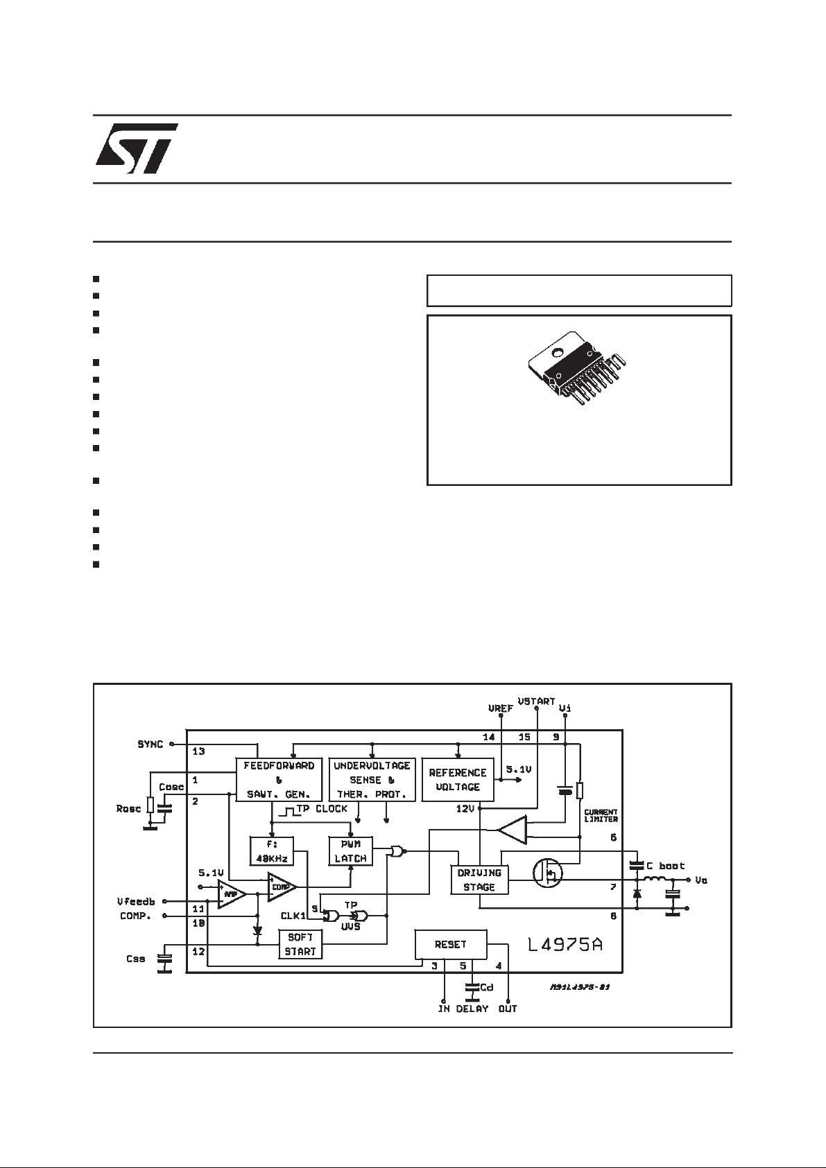
BLOCK DIAGRAM
MULTIPOWER BCD TECHNOLOGY
Multiwatt15V
ORDERING NUMBER:
Realized with BCD mixed technology, the device
uses a DMOS output transistortoobtainvery high
efficiency and very fast switching times. Features
of the L4975A include reset and power fail for microprocessors, feed forward line regulation, soft
start, limiting current and thermal protection. The
device is mounted in a 15-lead multiwatt plastic
power package and requires few external components. Efficient operation at switching frequencies
up to 500KHz allows reduction in the size and
costof externalfilter components.
L4975A
June 2000
This is advanced information on a new product now in development or undergoing evaluation. Details are subject to change without notice.
1/21
L4975A
ABSOLUTE MAXIMUM RATINGS
Symbol Parameter Value Unit
V
9
V
9
V
7
I
7
V
6
V
3,V12
V
4
I
4
V
5,V10,V11,V13
I
5
I
10
I
12
P
tot
,T
T
j
stg
Input Voltage 55 V
Input Operating Voltage 50 V
Output DC Voltage
Output Peak Voltage at t = 0.1µs f = 200KHz
-1
-7
Maximum Output Current Internally Limited
Bootstrap Voltage
Bootstrap Operating Voltage
65
V
+15
9
Input Voltage at Pins 3, 12 12 V
Reset Output Voltage 50 V
Reset Output Sink Current 50 mA
Input Voltage at Pin 5, 10, 11,13 7 V
Reset Delay Sink Current 30 mA
Error Amplifier Output SinkCurrent 1 A
Soft Start Sink Current 30 mA
Total Power Dissipation at T
< 120°C30W
case
Junction and Storage Temperature -40 to 150 °C
V
V
V
V
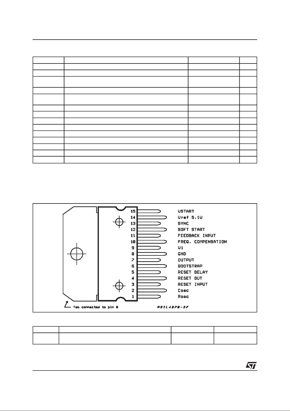
PIN CONNECTION
(Topview)
THERMAL DATA
Symbol Parameter Value Unit
R
th j-case
R
thj-amb
Thermal Resistance Junction-case max
Thermal Resistance Junction-ambient max
1
35
°C/W
°C/W
2/21
PIN FUNCTIONS
o
N
1 OSCILLATOR R
2 OSCILLATOR C
3 RESET INPUT Input of Power Fail Circuit. The threshold is 5.1V. It may be connected via a
4 RESET OUT Open Collector Reset/power Fail Signal Output. This output is high when the
5 RESET DELAY A C
6 BOOTSTRAP A C
7 OUTPUT Regulator Output.
8 GROUND Common Ground Terminal
9 SUPPLY VOLTAGE Unregulated Input Voltage.
10 FREQUENCY
COMPENSATION
11 FEEDBACK INPUT The Feedback Terminal of the Regulation Loop. The output is connected
12 SOFT START SoftStart Time Constant.A capacitor is connected betweenthi sterminal and
13 SYNC INPUT Multiple L4975A are synchronizedby connecting pin 13inputs together or via
14 V
15 V
Name Function
. External resistor connected to ground determines the constant charging
osc
ref
start
current of C
. External capacitor connected to ground determines (withR
osc
switching frequency.
divider to theinput for power fail function. It must be connected to the pin 14 an
external 30KΩ resistor when power fail signal not required.
supply and the output voltages are safe.
capacitor connected between this terminal and ground determines the
d
reset signal delay time.
boot
drive properly the internal D-MOS transistor.
A series RC network connected between this terminal and ground determines
the regulation loop gain characteristics.
directly to this terminal for 5.1V operation; It is connected via a divider for higher
voltages.
ground to define the soft start time constant.
an external syncr. pulse.
5.1V V
Internal Start-up Circuit to Drive the Power Stage.
.
osc
capacitor connected between this terminal and the output allows to
Device Reference Voltage.
ref
osc
) the
L4975A
CIRCUIT OPERATION
(refer to the block dia-
gram)
The L4975Ais a 5A monolithicstepdownswitching
regulator working in continuous mode realized in
the new BCD Technology. This technologyallows
the integration of isolated vertical DMOS power
transistorsplusmixedCMOS/Bipolartransistors.
The device can deliver 5A at an output voltage
adjustable from 5.1V to 40V, and contains diagnostic and control functions that make it particularly suitable for microprocessorbased systems.
BLOCK DIAGRAM
The block diagram shows the DMOS power transistor and the PWM control loop. Integrated functions include a reference voltage trimmed to 5.1V
± 2%, soft start, undervoltage lockout, oscillator
with feedforward control, pulse by pulse current
limit, thermal shutdown and finally the reset and
power fail circuit. The reset and power fail circuit
provides an output signal for a microprocessorindicating the statusof thesystem.
Device turn on is around 11V with a typical 1V
hysteresis, this threshold provides a correct voltage for the driving stage of the DMOS gate and
the hysteresispreventsinstabilities.
An external bootstrap capacitor charged to 12V
by an internal voltage reference is neededto provide correct gate drive to the power DMOS. The
driving circuit is able to source and sink peak currents of around 0.5A to the gate of the DMOS
transistor. A typical switching time of the current
in the DMOS transistor is 50ns. Due to the fast
commutation switching frequencies up to 500kHz
are possible.
The PWM control loop consists of a sawtooth oscillator, error amplifier, comparator, latch and the
output stage. An error signal is producedby comparing the output voltage with the precise 5.1V ±
2% on chip reference. This error signal is then
compared with the sawtooth oscillator, in order to
generate a fixed frequencypulse width modulated
drive for the output stage. A PWM latch is included to eliminate multiple pulsing within a period even in noisy environments. The gain and
3/21
L4975A
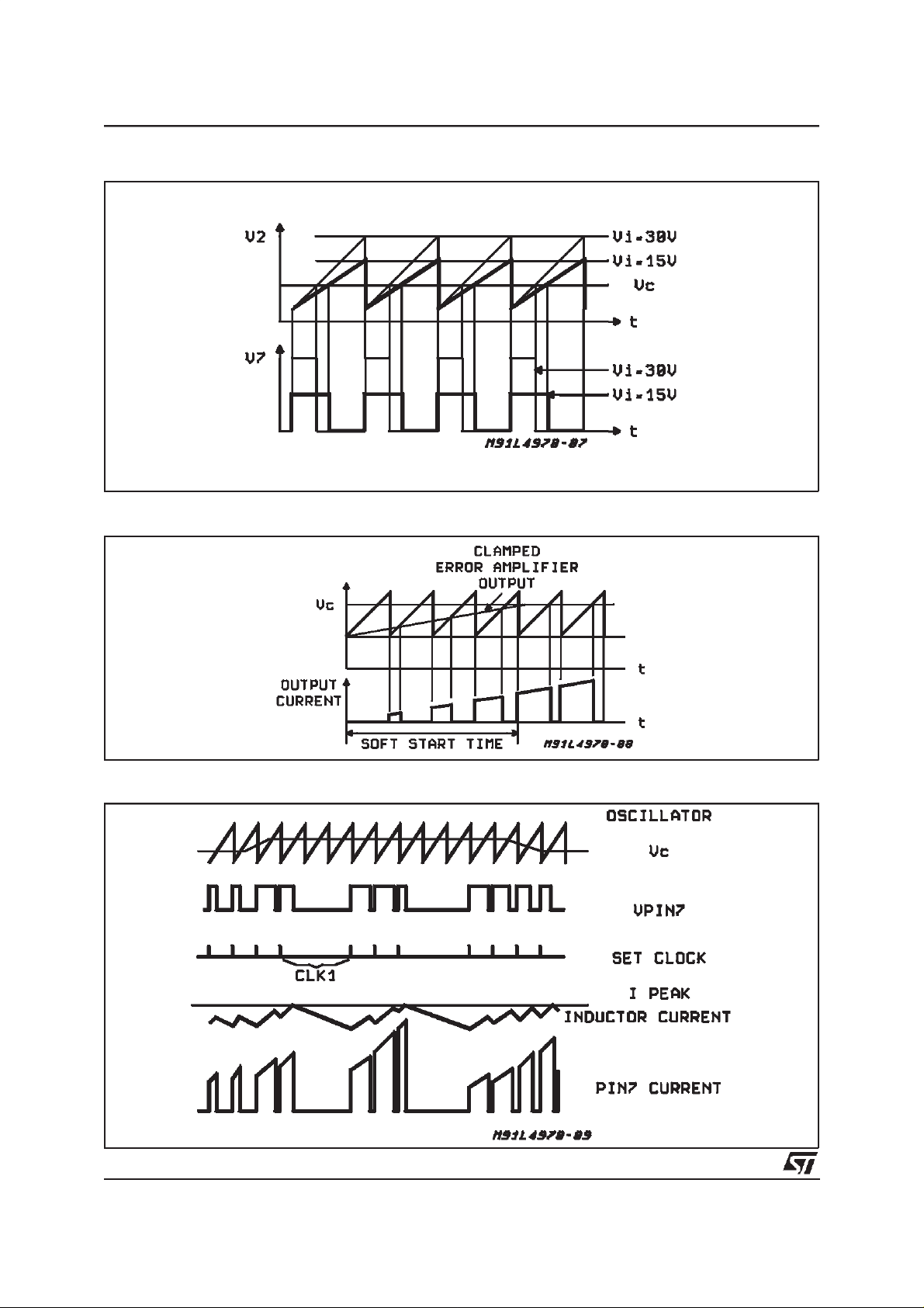
Figure 1:
Figure 2:
FeedforwardWaveform
Soft Start Function
Figure 3:
4/21
LimitingCurrent Function
L4975A
stability of the loop can be adjusted by an external RC network connected to the output of theerror amplifier. A voltage feedforward control has
been added to the oscillator, this maintains superior line regulation over a wide input voltage
range. Closing the loop directly gives an output
voltage of 5.1V, higher voltages are obtained by
inserting a voltagedivider.
At turn on output overcurrents are prevented by
the soft start function (fig. 2). The error amplifieris
initially clamped by an external capacitor Css and
allowed to rise linearly under the charge of an internalconstant current source.
Output overload protection is provided by a current limit circuit (fig. 3). The load current is sensed
by an internal metal resistor connected to a comparator. When the load current exceeds a preset
threshold the output of the comparator sets a flip
flop which turns off the power DMOS. The next
clock pulse, from an internal 40kHz oscillator will
reset the flip flop and the power DMOS will again
conduct. This current protection method, ensures
Figure 4:
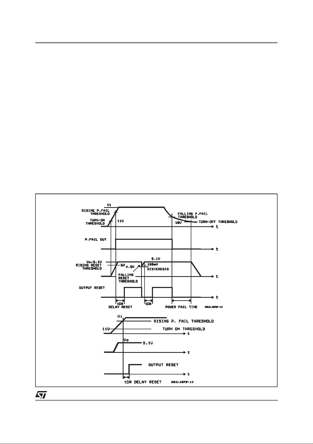
Resetand Power Fail Functions.
a constant current output when the system is
overloaded or short circuited and limits the
switchingfrequency,in this condition, to 40kHz.
The Reset and Power fail circuitry (fig 4) generates an output signal when the supply voltage exceeds a threshold programmed by an external
voltage divider. The reset signal, is generated
with a delay time programmed by an external capacitor on the delay pin. When the supply voltage
falls below the threshold or the output voltage
goes below 5V the reset output goes low immediately. The reset output is an open collector-drain.
Fig 4A showsthe case when the supplyvoltage is
higher than the threshold, but the output voltage
is not yet 5V.
Fig 4B shows the case when the output is 5.1V
but the supply voltage is not yet higher than the
fixedthreshold.
The thermal protection disables circuit operation
when the junction temperature reaches about
150°C and has an hysterysis to prevent unstable
conditions.
A
B
5/21
L4975A
ELECTRICALCHARACTERISTICS (Refer to the test circuit,Tj=25°C, Vi=35V, R4= 16KΩ,
= 2.2nF, fSW= 200KHztyp, unless otherwisespecified)
C
9
DYNAMICCHARACTERISTICS
Symbol Parameter TestCondition Min. Typ. Max. Unit Fig.
input Voltage Range (pin9) Vo=V
i
Output Votage Vi= 15V to 50V
Line Regulation Vi= 15V to 50V
o
Load Regulation Vo=V
o
I
o
I
o
I
o
V
∆V
∆
V
o
V
Io=2Ato4A
I
o
V
d
I
7L
Dropout Voltage Between
Pin 9 and 7
Io=3A
I
o
Max. Limiting Current Vi= 15 to 50V
V
η
Efficiency I
o
V
Vo= 12V
I
o
V
Vo= 12V
SVR Supply Voltage Ripple
Reject.
V
f = 100Hz; V
f Switching Frequency 180 200 220 KHz 5
f
∆
∆ V
∆ f
T
f
max
V
SECTION(pin 14)
ref
Voltage Stability of
Swiching Frequency
i
Temperature Stability of
Swiching Frequency
j
Maximum Operating
Switching Frequency
Vi= 15V to 45V 2 6 % 5
Tj= 0 to 125°C1%5
Vo=V
I
o
to 40V
ref
=5A
= 3A; Vo=Vref
= 2A; Vo=Vref
ref
=1Ato5A
=5A
to 40V
o=Vref
=3A
o=Vref
=5A
o=Vref
= 2VRMS; Io=3A
i
ref;R4
o=Vref
= 10KΩ
= 5A; C9= 1nF
15 50 V 5
5 5.1 5.2 V 5
12 30 mV 5
10
20
0.4
0.55
30
50
0.6
0.8
mV
mV
V
V
5.5 6.5 7.5 A 5
70 75
80
80 85
92
%
%
%
%
56 60 dB 5
500 KHz 5
5
5
5
5
Symbol Parameter TestCondition Min. Typ. Max. Unit Fig.
Reference Voltage 5 5.1 5.2 V 7
Line Regulation Vi= 15V to 50V 10 25 mV 7
14
Load Regulation I14= 0 to 1mA 20 40 mV 7
14
14
Average Temperature
T
=0°C to 125°C 0.4 mV/°C7
j
Coefficient Reference
∆
V
∆V
∆
14
V
V
∆T
Voltage
Short Circuit Current Limit V14= 0 70 mA 7
SECTION(pin 15)
V
START
I
14 short
Symbol Parameter TestCondition Min. Typ. Max. Unit Fig.
V
15
∆V
V
∆
I
15 short
Reference Voltage 11.4 12 12.6 V 7
Line Regulation Vi= 15 to 50V 0.6 1.4 V 7
15
Load Regulation I15= 0 to 1mA 50 200 mV 7
15
Short Circuit Current Limit V15=0V 80 mA 7
6/21
L4975A
ELECTRICALCHARACTERISTICS
(continued)
DC CHARACTERISTICS
Symbol Parameter TestCondition Min. Typ. Max. Unit Fig.
V
V
9on
9 Hyst
I
9Q
I
9OQ
I
7L
Turn-on Threshold 10 11 12 V 7A
Turn-off Hysteresys 1 V 7A
Quiescent Current V12=0; S1=D 13 19 mA 7A
Operating Supply Current V12= 0; S1 = C; S2 = B 16 23 mA 7A
Out Leak Current Vi= 55V; S3 = A; V12=0 2 mA 7A
SOFT START
Symbol Parameter Test Condition Min. Typ. Max. Unit Fig.
I
12
V
12
Soft Start Source Current V12= 3V; V11= 0V 70 100 130
Output Saturation Voltage I12= 20mA; V9= 10V
I
= 200µA; V9= 10V
12
1
0.7
A7B
µ
V
V
ERRORAMPLIFIER
Symbol Parameter Test Condition Min. Typ. Max. Unit Fig.
V
10H
V
10L
I
10H
I
10L
I
11
G
SVR Supply Voltage Rejection 15 < V
V
OS
High Level Out Voltage I10= -100µA; S1 = C
V
= 4.7V
11
Low Level Out Voltage I10= +100µA; S1 = C
V
= 5.3V;
11
Source Output Current V10= 1V; S1 = E
V
= 4.7V
11
Sink Output Current V10 = 6V; S1 = D
V
= 5.3V
11
6V7C
1.2 V 7C
100 150
A7C
µ
100 150 µA7C
Input Bias Current RS= 10KΩ 0.4 3 µA–
DC Open Loop Gain V
V
R
R
VCM
=10Ω
S
=10Ω
S
= 4V;
< 50V;
i
60 dB –
60 80 dB –
Input Offset Voltage RS=50Ω 210mV–
RAMP GENERATOR(pin 2)
7B
7B
Symbol Parameter Test Condition Min. Typ. Max. Unit Fig.
V
2
V
2
I
2
I
2
Ramp Valley S1 = C; S2 = B 1.2 1.5 V 7A
Ramp Peak S1 = C Vi= 15V
S2 = B V
= 45V
i
Min. Ramp Current S1 = A; I1= 100µA 270 300
2.5
5.5
V
V
A7A
µ
Max. Ramp Current S1 = A; I1 = 1mA 2.4 2.7 mA 7A
SYNC FUNCTION(pin 13)
Symbol Parameter Test Condition Min. Typ. Max. Unit Fig.
V
13
V
13
I
13L
I
13H
V
13
t
W
Low Input Voltage Vi= 15V to 50V; V12=0;
S1 = C; S2 = B; S4 = B
High Input voltage V12=0;
S1 = C; S2 = B; S4 = B
Sync Input Current with
Low Input Voltage
Input Current with High
Input Voltage
V2=V13= 0.9V; S4= A;
S1 = C; S2 = B
V13= 3.5V; S4 = A;
S1 = C; S2 = B
Output Amplitude 4 5 V –
Output Pulse Width V
= 2.5V 0.3 0.5 0.8 µs–
thr
–0.3 0.9 V 7A
3.5 5.5 V 7A
0.4 mA 7A
2mA7A
7A
7A
7/21

L4975A
ELECTRICALCHARACTERISTICS
(continued)
RESET AND POWER FAIL FUNCTIONS
Symbol Parameter Test Condition Min. Typ. Max. Unit Fig.
V
11R
V
11F
V
5H
V
5L
–I
5SO
I
5SI
V
4S
I
4
V
3R
V
3H
I
3
Rising Threshold Voltage
(pin 11)
Falling Threshold Voltage
(pin 11)
Delay High Threshold
Voltage
Delay Low Threshold
Voltage
Delay Source Current V3= 5.3V; V5=3V 40 60 80 µA7D
Delay Sink Current V3= 4.7V; V5=3V 10 mA 7D
Out Saturation Voltage I4= 15mA; S1 = B
Output Leak Current V4= 50V; S1 = A
Rising Threshold Voltage V11=V
Hysteresys 0.4 0.5 0.6 V 7D
Input Bias Current 1 3 µA7D
Vi= 15 to 50V
V
= 5.3V
3
Vi = 15 to 50V
V
= 5.3V
3
Vi= 15 to 50V
V
11=V14
Vi = 15 to 50V
V
11=V14
V
= 4.7V
3
V
= 5.3V
3
14
V3= 5.3V
V
ref
–120
4.77 V
V
ref
–100
ref
–200
V
ref
–80
V
ref
–160
V
mV
V
mV
4.95 5.1 5.25 V 7D
1 1.1 1.2 V 7D
0.4 V 7D
100 µA7D
4.95 5.1 5.25 V 7D
Figure 5: Test and EvaluationBoard Circuit
7D
7D
TYPICAL PERFORMANCES (using evaluationboard) :
n = 83% (V
V
o RIPPLE
Line regulation = 5mV (V
Load regulation= 15mV(I
= 35V ; Vo=V
i
REF;Io
=5A;fSW= 200KHz)
= 30mV(at 5A) with outputfilter capacitor ESR ≤ 60mΩ
= 15 to 50V)
i
= 2 to 5A)
o
For componentvalues, refer to test circuit partlist.
8/21

L4975A
Figure 6a:
P.C.Board (components side) and ComponentsLayout of Figure 5 (1:1 scale).
PARTS LIST
R1= 30K
R
R
R
R
R
R
R
R
R
R
Ω
= 10KΩ C3,C4,C5,C6= 2.2µF
2
= 15KΩ C7= 390pF Film
3
= 16KΩ C8= 22nF MKT 1817 (ERO)
4
=22Ω0,5W
5
= 4K7 C9= 2.2nF KP1830
6
=10Ω C10= 220nF MKT
7
= see tab. A C11= 2.2nF MP1830
8
= OPTION **C12,C13,C14= 220µF 40VLEKR
9
= 4K7 C15=1µF Film
10
=10Ω
11
D1 = MBR 760CT (or 7.5A/60V or equivalent)
L1 = 80µH core 58930 MAGNETICS
* 2 capacitors in parallel to increase input RMS current capability
** 3 capacitors in parallel to reduce total output ESR
C1,C2= 3300µF 63VLEYF (ROE
24 TURNS Ø 1.1mm (AWG 17)
COGEMA 949178
Table A
V
12V
15V
18V
24V
0
R
9
4.7k
4.7kΩ
4.7kΩ
4.7kΩ
R
7
Ω
6.2kW
9.1kΩ
12kΩ
18kΩ
Table B
SUGGESTEDBOOTSTRAPCAPACITORS
Operating Frequency Bootstrap Cap.c10
f = 20KHz ≥680nF
f = 50KHz
f = 100KHz
f = 200KHz ≥220nF
f = 500KHz ≥100nF
470nF
≥
330nF
≥
9/21
L4975A
Figure 6b: P.C. Board (Back side) and ComponentsLayout of the Circuit of Fig. 5. (1:1 scale)
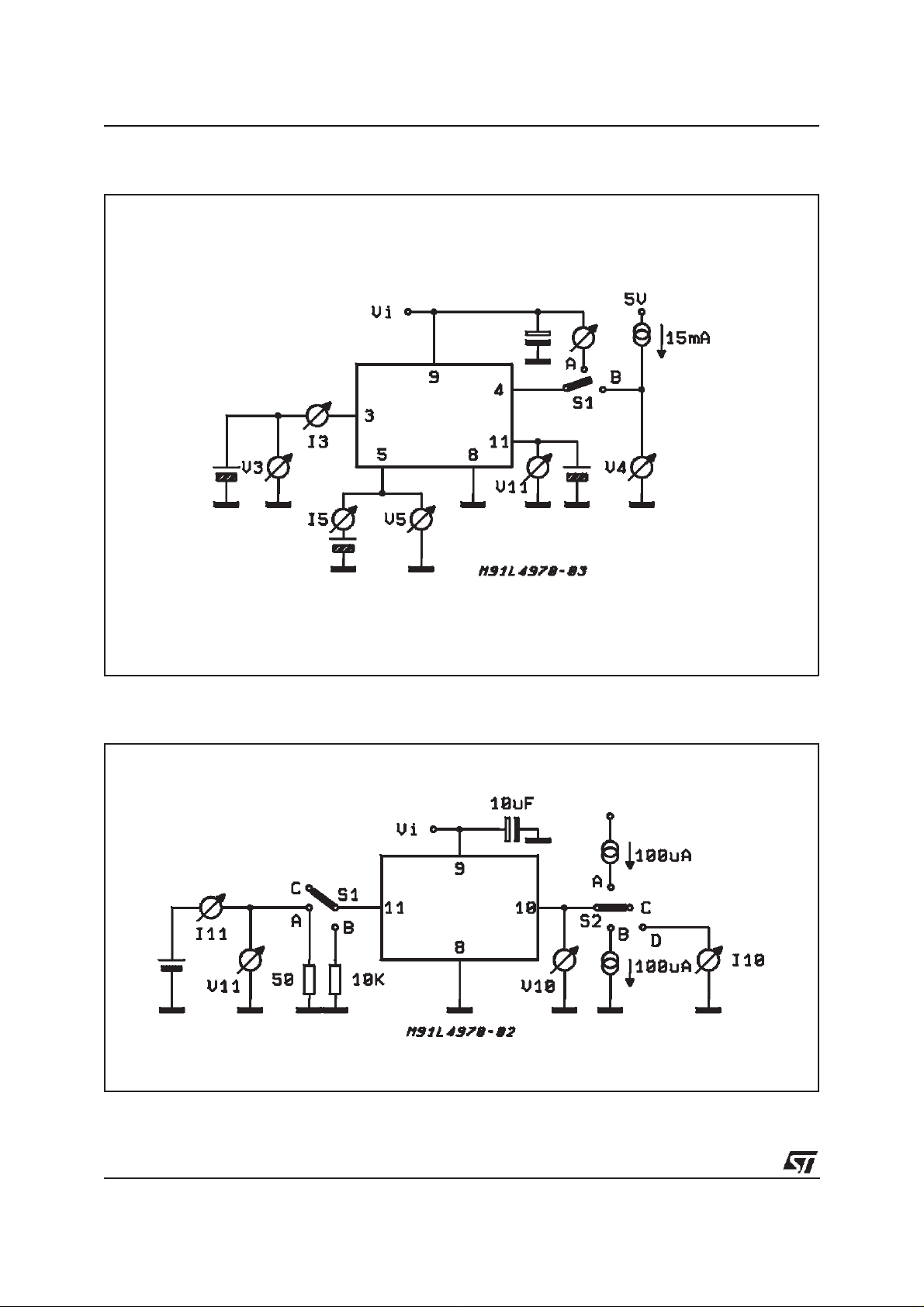
Figure 7: DC Test Circuits
10/21

Figure 7A
L4975A
Figure 7B
11/21
L4975A
Figure 7D
Figure 7C
12/21

L4975A
Figure 8: QuiescentDrain Current vs. Supply
Voltage(0% duty cycle- see fig. 7A).
Figure 10: QuiescentDrain Currentvs. Duty
Cycle
Figure9: QuiescentDrain Current vs. Junction
Temperature(0% duty cycle).
Figure11:
ReferenceVoltage (pin14) vs. V
(see
i
fig. 7)
Figure 12: ReferenceVoltage (pin 14) vs.
Junction Temperature (see fig. 7)
Figure13: ReferenceVoltage (pin15) vs. V
fig. 7)
(see
i
13/21

L4975A
Figure 14: ReferenceVoltage (pin 15) vs.
Junction Temperature (see fig. 7)
Figure 16: SwitchingFrequencyvs. Input
Voltage(see fig. 5)
Figure15: ReferenceVoltage 5.1V (pin 14)
SupplyVoltage Ripple Rejectionvs.
Frequency
Figure17: SwitchingFrequency vs. Junction
Temperature(see fig 5)
Figure 18: SwitchingFrequencyvs. R4 (seefig. 5)
14/21
Figure19:
Max.Duty Cycle vs. Frequency

L4975A
Figure 20: Supply Voltage Ripple Rejection vs.
Frequency(see fig. 5)
Figure 22: LoadTransient Response (see fig. 5)
Figure21: Line Transient Response (see fig. 5)
Figure23:
DropoutVoltage Between Pin 9 and
Pin 7 vs. Current at Pin 7
Figure 24: DropoutVoltage Between Pin 9 and
Pin 7 vs.Junction Temperature
Figure25: PowerDissipation (device only) vs.
Input Voltage
15/21

L4975A
Figure 26: Power Dissipation (deviceonly) vs.
OutputVoltage
Figure 28: Efficiencyvs. Output Current
Figure27: HeatsinkUsedto Derivethe Device’s
PowerDissipation
- Heatsink=
R
th
case
amb
P
d
− T
T
Figure29: Efficiencyvs. Output Voltage
Figure 30:
16/21
Efficiencyvs. Output Voltage
Figure31: OpenLoop Frequencyand Phase
Responseof Error Amplifier (see
fig.7C)

L4975A
Figure 32:
PowerDissipationDeratingCurve
Figure 33: 5.1V/12VMultiple Supply. Note the Synchronizationbetween the L4975A and the L4974A
17/21
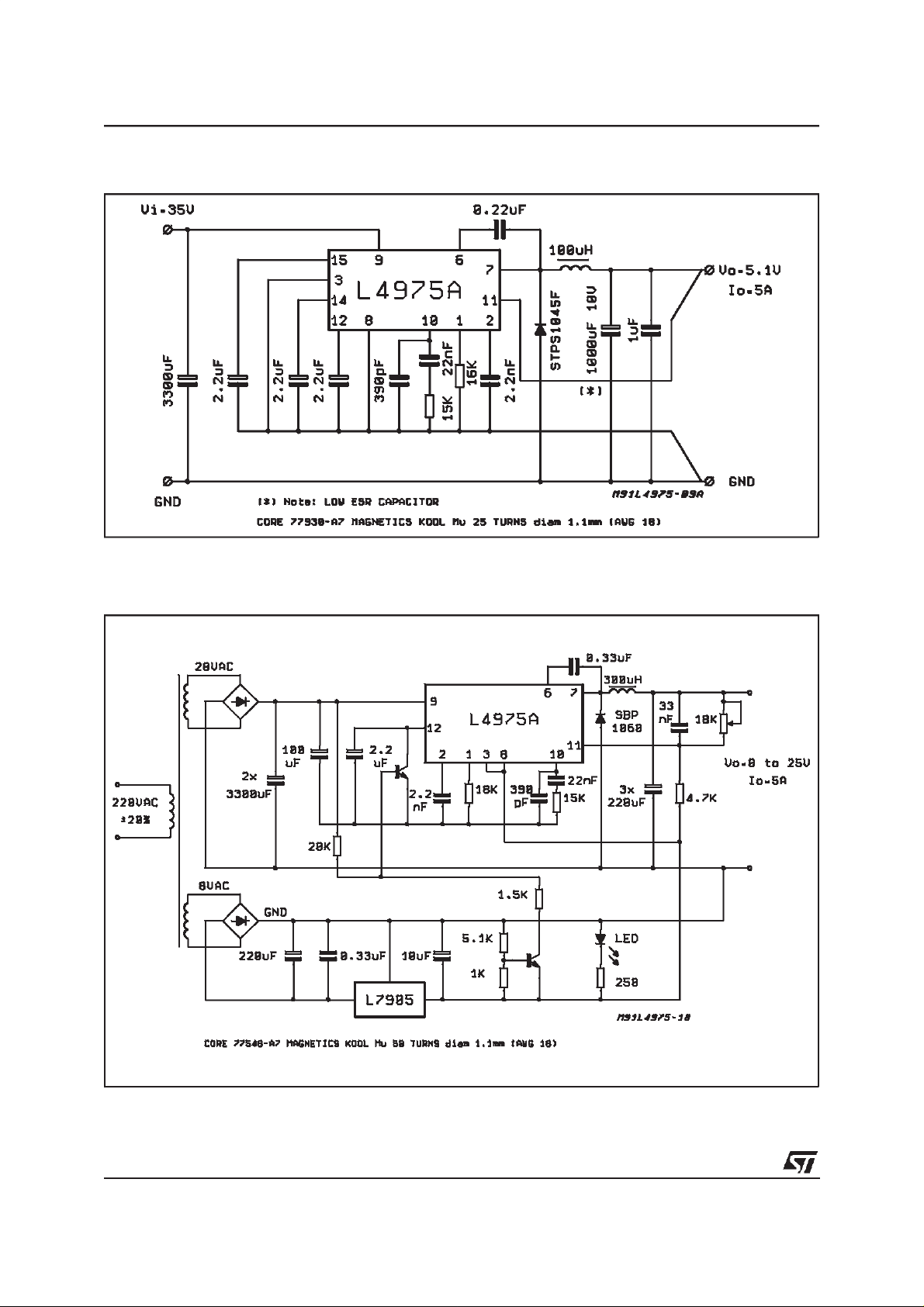
L4975A
Figure 34: 5.1V / 5A Low Cost Application
Figure 35: 5A SwitchingRegulator,Adjustablefrom 0V to 25V.
18/21

Figure 36: L4975A’sSync. Example
L4975A
19/21

L4975A
DIM.
Dia1 3.65 3.85 0.144 0.152
MIN. TYP. MAX. MIN. TYP. MAX.
A5
B 2.65 0.104
C 1.6 0.063
D 1 0.039
E 0.49 0.55 0.019 0.022
F 0.66 0.75 0.026 0.030
G 1.02 1.27 1.52 0.040 0.050 0.060
G1 17.53 17.78 18.03 0.690 0.700 0.710
H1 19.6 0.772
H2 20.2 0.795
L 21.9 22.2 22.5 0.862 0.874 0.886
L1 21.7 22.1 22.5 0.854 0.870 0.88
L2 17.65 18.1 0.695
L3 17.25 17.5 17.75 0.679 0.689 0.699
L4 10.3 10.7 10.9 0.406 0.421 0.429
L7 2.65 2.9 0.104 0.114
M 4.25 4.55 4.85 0.167 0.179 0.191
M1 4.63 5.08 5.53 0.182 0.200 0.218
S 1.9 2.6 0.075 0.102
S1 1.9 2.6 0.075 0.102
mm inch
0.197
0.713
OUTLINE AND
MECHANICAL DATA
6
Multiwatt15 V
20/21

L4975A
Information furnished is believed to be accurate and reliable. However, STMicroelectronics assumes no responsibility for the consequences
of use of such information nor for any infringement of patents or other rights of third parties which may result from its use. No license is
granted by implication or otherwise under any patent or patent rights of STMicroelectronics. Specification mentioned in this publication are
subject to change without notice. This publication supersedes and replaces all information previously supplied. STMicroelectronics products
are not authorized for use as critical components in life support devices or systems without express written approval of STMicroelectronics.
The ST logo is a registered trademark of STMicroelectronics
2000 STMicroelectronics – Printed in Italy– All Rights Reserved
STMicroelectronics GROUP OF COMPANIES
Australia - Brazil - China- Finland - France - Germany - HongKong - India - Italy - Japan - Malaysia - Malta - Morocco -
Singapore - Spain - Sweden - Switzerland - United Kingdom - U.S.A.
http://www.st.com
21/21
 Loading...