

SGS Thomson Microelectronics L4972AD, L4972A Datasheet
L4972A
.
2AOUTPUTCURRENT
.5.1VTO40VOUTPUTVOLTAGERANGE
.
0 TO 90%DUTY CYCLERANGE
.INTERNALFEED-FORWARD LINEREG.
.INTERNALCURRENT LIMITING
.PRECISE5.1V± 2% ONCHIPREFERENCE
.RESETAND POWERFAILFUNCTIONS
.
INPUT/OUTPUTSYNC PIN
.UNDER VOLTAGE LOCK OUT WITH HYS-
TERETICTURN-ON
.PWM LATCH FOR SINGLE PULSE PER PE-
RIOD
.VERYHIGH EFFICIENCY
.SWITCHINGFREQUENCYUP TO 200KHz
.THERMAL SHUTDOWN
.CONTINUOUSMODE OPERATION
DES CRIPTI ON
TheL4972Aisa stepdownmonolithicpowerswitchingregulatordelivering2Aat avoltagevariablefrom
5.1 to 40V.
Realized with BCD mixed technology, the device
uses a DMOS output transistorto obtain very high
efficiencyandveryfastswitchingtimes.Featuresof
L4972AD
2A SWITCHINGREGULATOR
MULTIPO WER BCD TECHNOLO GY
POWERD IP
(16 + 2 + 2)
ORDERING NUMBERS : L4972A(Powerdip)
L4972AD (SO20)
the L4972A include reset and power fail for microprocessors,feed forward line regulation,soft start,
limitingcurrent and thermalprotection. The device
ismountedina Powerdip16+2+2and SO20large
plasticpackagesand requiresfew externalcomponents. Efficient operation at switching frequencies
up to 200KHzallowsreduction in the size and cost
of externalfiltercomponent.
SO20
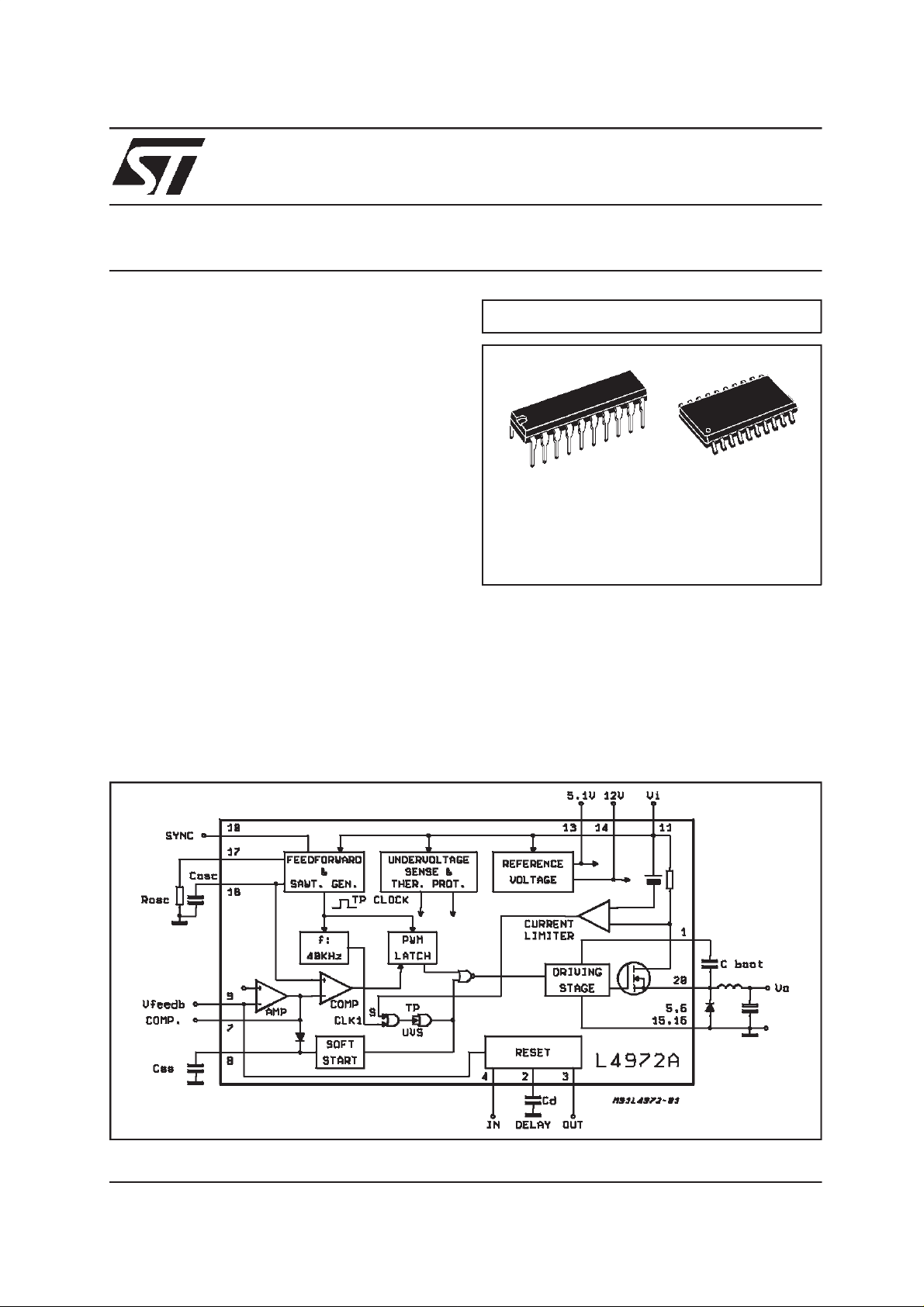
BLOCK DIAGRAM
June 2000
This is advanced information on a new product now in development or undergoing evaluation. Details are subject to change without notice.
1/23
L4972A-L4972AD
ABSOLU TE MAX IMUM RATINGS
Symbol Parameter Valu e Unit
V
V
V
I
V
4,V8
V
V
2,V7,V9,V10
P
T
J,Tstg
(*) SO-20
11
11
20
20
V
I
3
I
3
I
2
I
7
I
8
tot
InputVoltage 55 V
InputOperatingVoltage 50 V
OutputDC Voltage
OutputPeak Voltageat t = 0.1µs f = 200khz
-1
-5
Maximum Output Current Internally Limited
BoostrapVoltage
BoostrapOperating Voltage
65
V
+15
11
InputVoltage at Pins4, 12 12 V
Reset Output Voltage 50 V
Reset Output Sink Current 50 mA
InputVoltage at Pin 2, 7, 9, 10 7 V
Reset Delay Sink Current 30 mA
ErrorAmplifier Output Sink Current 1 A
Soft Start Sink Current 30 mA
TotalPower Dissipation at T
at T
90°C
≤
PINS
=70°C(No copper area on PCB)
amb
5 / 3.75(*)
1.3/1(*)
Junctionand Storage Temperature -40 to 150 °C
V
V
V
V
W
W
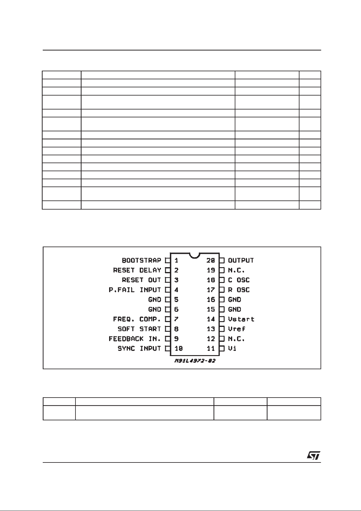
PI N CO NNECTI O N (top v iew)
THERMAL DATA
Symbol Parame t er Po w erd ip SO- 20
R
th j-pins
R
thj-amb
Thermal ResistanceJunction-Pins max
Thermal ResistanceJunction-ambient max
12°C/W
60°C/W
16°C/W
80°C/W
2/23
L4972A-L4972AD
PIN FUNCTIONS
o
N
1 BOOTSTRAP A C
2 RESET DELAY A C
3 RESET OUT Open CollectorReset/powerFailSignal Output.This output is highwhen the supply
4 RESET INPUT Input of Power Fail Circuit. The threshold is 5.1V. It may be connected via a divider
5, 6
GROUND Common GroundTerminal
15,16
7 FREQUENCY
COMPENSATION
8 SOFT START Soft StartTime Constant.A capacitoris connectedbetweenthi sterminaland ground
9 FEEDBACK INPUT The Feedback Terminal of the Regulation Loop. The output is connecteddirectly to
10 SYNC INPUT Multiple L4972A’s are synchronized by connecting pin 10 inputs together or via an
11 SUPPLYVOLTAGE Unregulated InputVoltage.
12,19 N.C. Not Connected.
13 V
14 V
ref
start
17 OSCILLATOR R
18 OSCILLATOR C
20 OUTPUT Regulator Output.
Name Function
capacitor connected between this terminal and the output allows to drive
boot
properlythe internalD-MOS transistor.
capacitor connected between this terminal and ground determines the reset
d
signaldelay time.
and theoutput voltages are safe.
tothe inputforpowerfailfunction.It mustbe connectedto thepin 14 an external30K
resistorwhen power fail signal not required.
A series RC network connected between this terminal and ground determines the
regulation loop gain characteristics.
to define the soft start time constant.
thisterminal for5.1V operation; It is connected via a dividerfor higher voltages.
externalsyncr. pulse.
5.1VV
DeviceReferenceVoltage.
ref
InternalStart-up Circuit to Drive the PowerStage.
. Externalresistorconnected to grounddeterminestheconstantchargingcurrent
osc
of C
.
osc
. External capacitor connected to ground determines (with R
osc
frequency.
) the switching
osc
Ω
3/23

L4972A-L4972AD
CIRCU I T OP ER ATION
The L4972Ais a 2A monolithicstepdownswitching
regulatorworkingincontinuousmoderealizedinthe
new BCD Technology.This technologyallows the
integrationofisolatedverticalDMOSpowertransistors plusmixedCMOS/Bipolartransistors.
The device candeliver 2A at an outputvoltage adjustable from 5.1V to 40V and contains diagnostic
and control functionsthat make it particularly suitable for microprocessorbased systems.
BLOCKDIAGRAM
The block diagram shows theDMOSpowertran-
sistorsand the PWM control loop.Integratedfunctions include a reference voltage trimmed to 5.1V
±2%,softstart,undervoltagelockout,oscillatorwith
feedforward control, pulse by pulse current limit,
thermal shutdown and finally the reset and power
fail circuit.The reset and power failcircuit provides
an outputsignalfora microprocessorindicatingthe
statusof the system.
Deviceturn on is around11V witha typical1Vhysterysis,thisthresholdporvidesa correctvoltagefor
the driving stageof the DMOS gateand the hysterysispreventsinstabilities.
Anexternalbootstrapcapacitorchargeto 12Vbyan
internalvoltagereferenceis neededto providecorrect gatedriveto the powerDMOS.Thedrivingcircuit is able to source and sink peak currents of
around0.5A to the gate of the DMOStransistor.A
typical switching time of the current in the DMOS
transistor is 50ns. Due to the fast commutation
switchingfrequenciesup to 200kHzare possible.
The PWMcontrolloop consistsof a sawtoothoscillator,erroramplifier,comparator,latch andthe outputstage.An errorsignalis producedbycomparing
theoutputvoltagewiththeprecise5.1V± 2%onchip
reference.This error signal is then comparedwith
the sawtooth oscillator in order to generate frixed
frequencypulsewidth modulateddrive for the output stage. A PWM latch is included to eliminate
multiple pulsingwithin a period even in noisy environments.
Thegainand stabilityoftheloopcanbe adjustedby
an externalRC networkconnectedto the outputof
the error amplifier. A voltage feedforward control
has beenaddedto the oscillator,this maintainssuperior line regulation over a wide input voltage
range.Closingthe loopdirectlygivesan outputvoltageof 5.1V,highervoltagesareobtainedbyinserting a voltagedivider.
Atturnon,outputovercurrentsarepreventedbythe
soft start function (fig. 2). The error amplifier is initiallyclampedbyan externalcapacitor,Css,and allowedto riselinearlyunderthe chargeof aninternal
constantcurrentsource.
Outputoverloadprotectionis providedby a current
limitcircuit. Theloadcurrentis sensedby a internal
metalresistorconnectedtoa comparator.Whenthe
loadcurrentexceedsa presetthreshold,the output
of the comparatorsetsa flipflop whichturns offthe
powerDMOS.Thenextclockpulse,fromaninternal
40kHzoscillator,willresettheflipflopandthepower
DMOS will again conduct. This current protection
method,ensuresaconstantcurrentoutputwhenthe
systemis overloadedorshortcircuitedandlimitsthe
switchingfrequency,inthiscondition,to40kHz.The
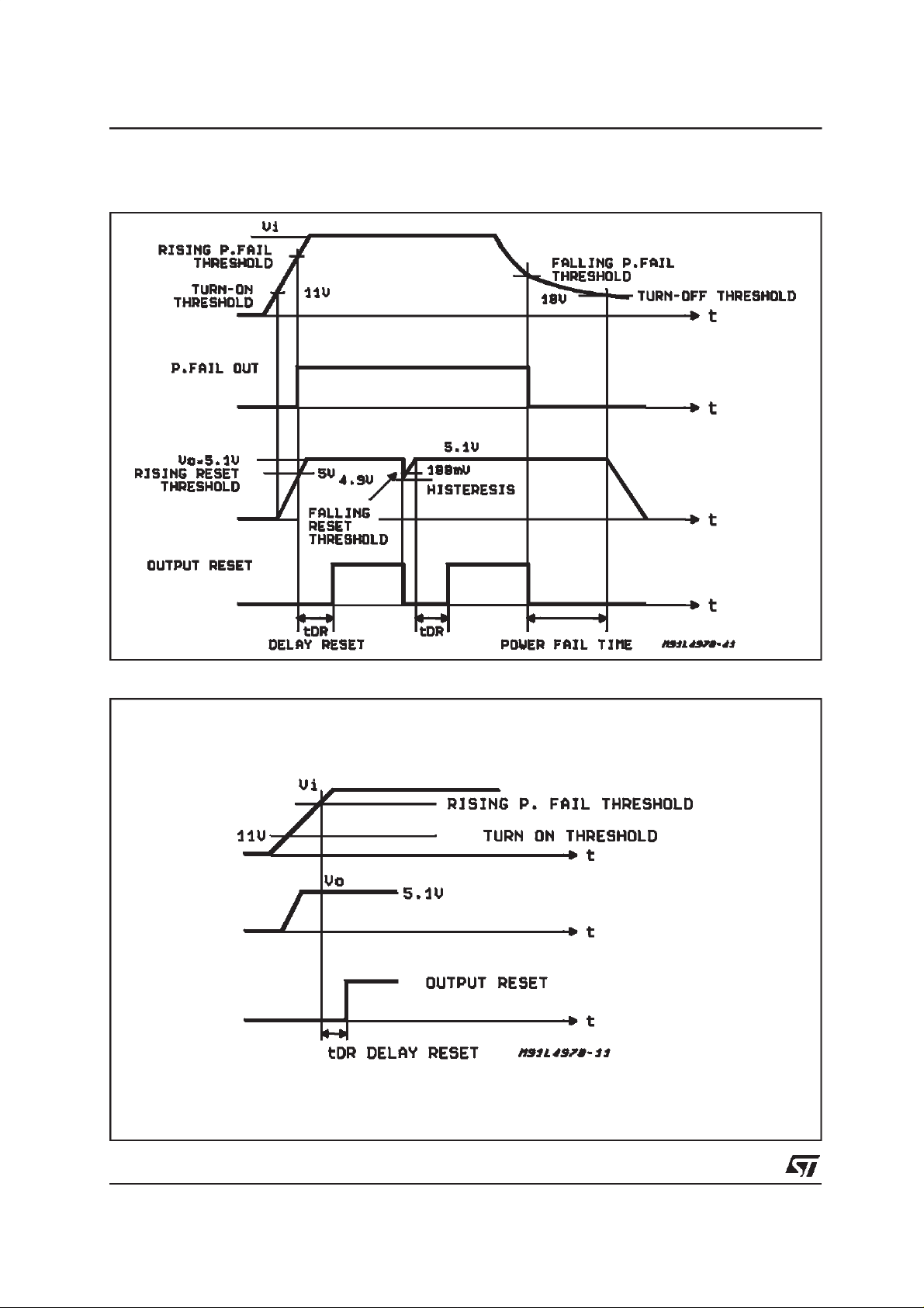
Reset and Power fail circuit (fig. 4), generatesan
output signal when the supply voltage exceeds a
threshold programmed by an external voltage divider. The reset signal, is generated with a delay
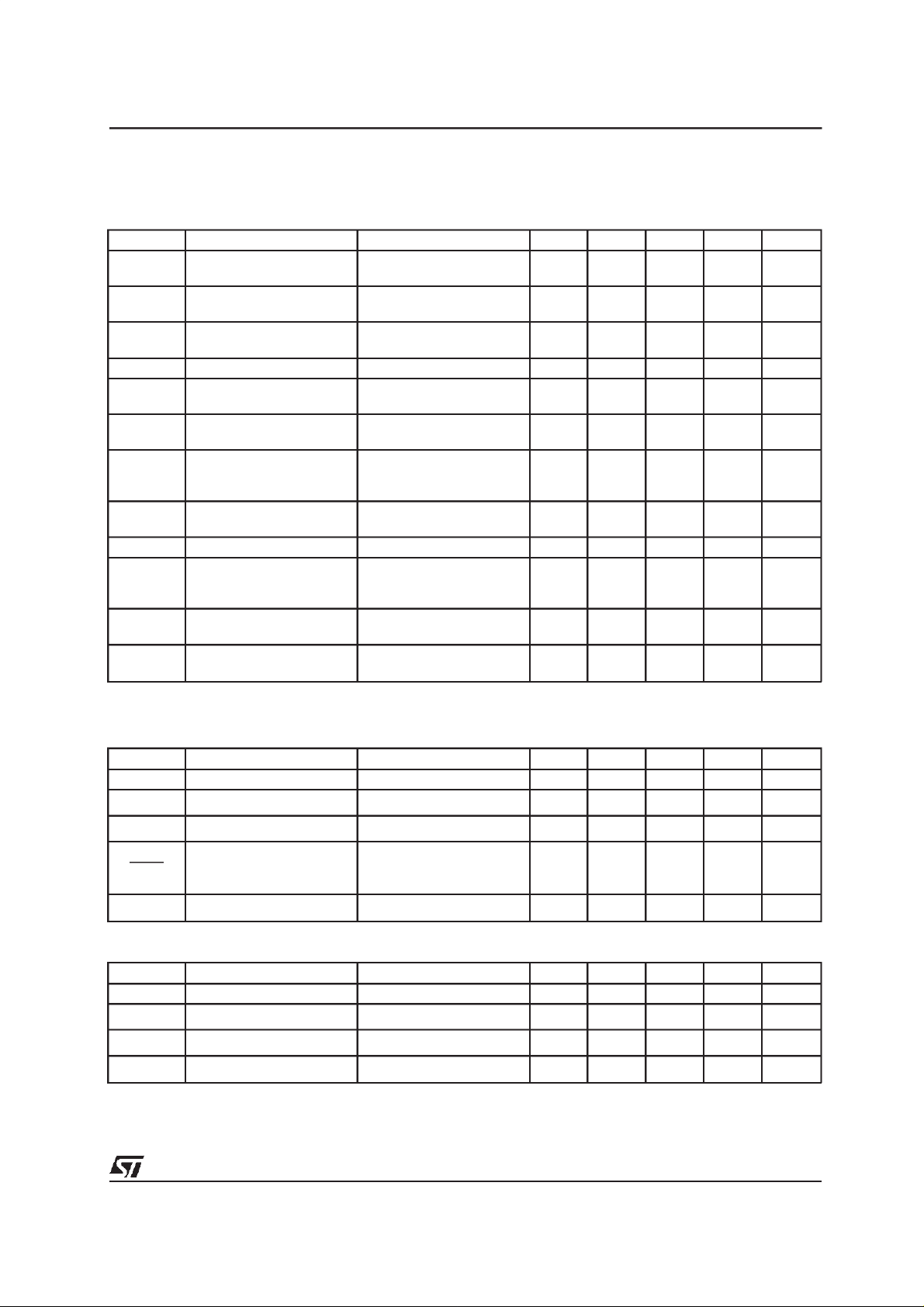
timeprogrammedbya externalcapacitoronthedelay pin. When the supply voltage falls below the
thresholdor the output voltagegoes below 5V, the
resetoutputgoeslowimmediately.Theresetoutput
is an opendrain.
Fig. 4A shows thecasewhen the supplyvoltageis
higherthan the threshold,but the output voltage is
not yet 5V.
Fig.4Bshowsthecasewhentheoutputis 5.1V,but
the supply voltage is not yet higherthan the fixed
threshold.
The thermal protection disables circuit operation
when the junction temperature reaches about
150°C and has a hysterysis to prevent unstable
conditions.
4/23
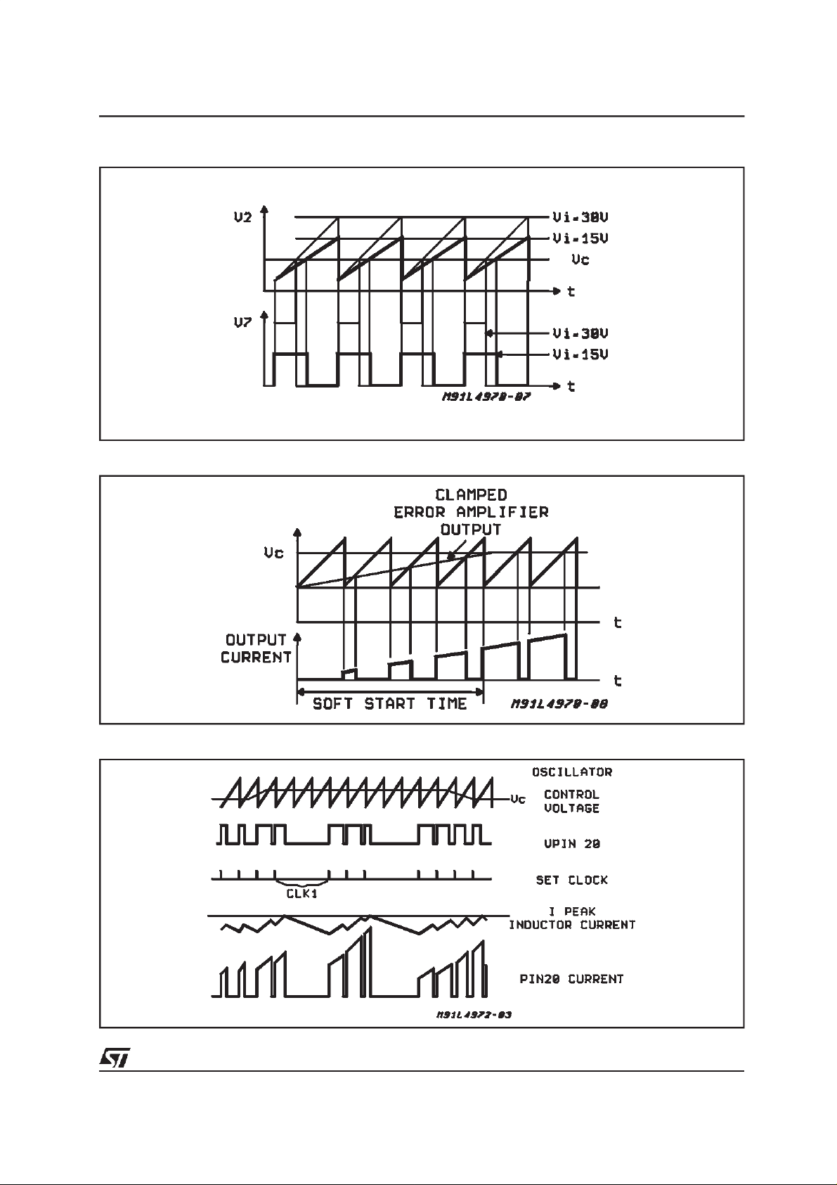
Figure1 : FeedforwardWaveform.
Figure2 : SoftStart Function.
L4972A-L4972AD
Figure3 : LimitingCurrentFunction.
5/23
L4972A-L4972AD
Figure4 : Resetand PowerFail Functions.
A
B
6/23
L4972A-L4972AD
ELECTRICALCHARACTERISTICS (referto the test circuit,TJ=25°C, Vi=35V, R4= 30KΩ,
= 2.7nF,fSW= 100KHztyp, unless otherwisespecified)
C
9
DYNAMICCHARACTERISTICS
Symbol Parameter Test Conditions Min. Typ. Max. Unit Fig.
V
V
∆V
∆V
V
InputVolt. Range (pin 11) Vo=V
i
OutputVoltage Vi=15V to 50V
o
Line Regulation Vi= 15V to 50V
o
Load Regulation Vo =V
o
Dropout Voltage between
d
I
o
I
o
I
o
Io= 2A 0.25 0.4 V
Pin11 and 20
I
20L
Max Limiting Current Vi= 15V to 50V
V
η
Efficiency (*) I
o
V
Vo= 12V
SVR Supply VoltageRipple
Rejection
V
f = 100Hz; V
f SwitchingFrequency 90 100 110 KHz 5
Vi Voltage Stability of
∆f/∆
V
Switching
Frequency
f/T
∆
Temperature Stability of
j
Tj=0 to 125°C1%5
SwitchingFrequency
f
max
(*) Only for DIP version (**) Pulse testing with a low duty cycle
Maximum Operating
SwitchingFrequency
Vo=V
I
o
ref
to 40V
15 50 V 5
= 2A (**)
5 5.1 5.2 V 5
= 1A;Vo=V
ref
12 30 mV
= 0.5A; Vo=V
refIo
ref
= 0.5Ato 2A 7 20 mV
2.5 2.8 3.5 A
to 40V
o=Vref
= 2A,f = 100KHz
o=Vref
75 85
90
= 2VRMS;Io=1A
i
= 15V to 45V 2 6 % 5
i
refR4
o=Vref
= 15K
Ω
56 60 dB 5
200 KHz 5
%
%
=2AC9= 2.2nF
V
SECTION(pin13)
ref
Symbol Parameter Test C o n di tion Mi n . Typ. Max. Uni t Fig.
V
∆
∆V
∆ V
∆
13
V
T
ReferenceVoltage 5 5.1 5.2 V 7
Line Regulation Vi= 15V to 50V 10 25 mV 7
13
Load Regulation I13 = 0 to 1mA 20 40 mV 7
13
Average Temperature
13
T
=0°C to 125°C 0.4 mV/°C7
j
CoefficientReference
Voltage
ShortCircuit Current Limit V13= 0 70 mA 7
SECTION(pin15)
V
START
I
13 short
Symbol Parameter Test C o n di tion Mi n . Typ. Max. Uni t Fig.
V
V
∆
V
∆
I
14 short
14
ReferenceVoltage 11.4 12 12.6 V 7
Line Regulation Vi= 15 to 50V 0.6 1.4 V 7
14
Load Regulation I14= 0 to 1mA 50 200 mV 7
14
ShortCircuit Current Limit V15=0V 80 mA 7
7/23
 Loading...