1.5A STEP DOWN SWITCHING REGULATOR
UP TO 1.5A STEPDOWN CONVERTER
OPERATINGINPUT VOLTAGE FROM 8V TO
55V
PRECISE 3.3V (±1%) INTERNAL REFER-
ENCE VOLTAGE
OUTPUT VOLTAGE ADJUSTABLE FROM
3.3VTO 50V
SWITCHINGFREQUENCY ADJUSTABLE UP
TO 500KHz
VOLTAGEFEEDFORWARD
ZEROLOAD CURRENTOPERATION
INTERNAL CURRENT LIMITING (PULSE-BY-
PULSEAND HICCUPMODE)
INHIBIT FOR ZERO CURRENT CONSUMP-
TION
PROTECTION AGAINST FEEDBACK DIS-
CONNECTION
THERMAL SHUTDOWN
SOFTSTART FUNCTION
DESCRIPTION
The L4971 is a step down monolithic power
switching regulator delivering 1.5A at a voltage
between 3.3V and 50V (selected by a simple external divider). Realized in BCD mixed technology, the device uses an internal power D-MOS
transistor (with a typical Rdson of 0.25Ω)toobtainvery high efficency and high switchingspeed.
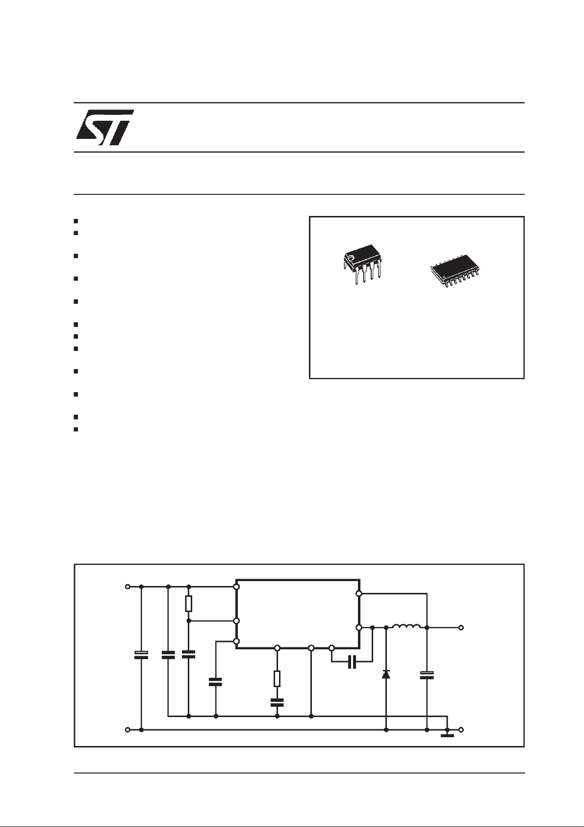
TYPICAL APPLICATIONCIRCUIT
L4971
Minidip SO16W
ORDERING NUMBERS: L4971 (Minidip)
L4971D (SO16)
A switching frequency up to 500KHz is achievable (the maximum power dissipation of the packages must be observed).
A wide input voltage range between 8V to 55V
and output voltages regulated from 3.3V to 50V
cover the majority of today’sapplications.
Features of this new generations of DC-DC converter include pulse-by-pulse current limit, hiccup
mode for short circuit protection, voltage feedforward regulation, soft-start, protection against
feedback loop disconnection, inhibit for zero current consumption and thermal shutdown.
The device is available in plastic dual in line,
MINIDIP 8 for standard assembly, and SO16W
for SMD assembly.
May 2000
Vi=8V to 55V
C1
220µF
63V
C7
220nF
R1
20K
C2
2.7nF
C5
100nF
5
3
2
L4971
7
R2
9.1K
22nF
1
C4
6
C6
100nF
D97IN748A
8
4
D1
GI
SB360
L1
126µ
H
(77120)
C
330µF
VO=3.3V/1.5A
8
1/12

L4971
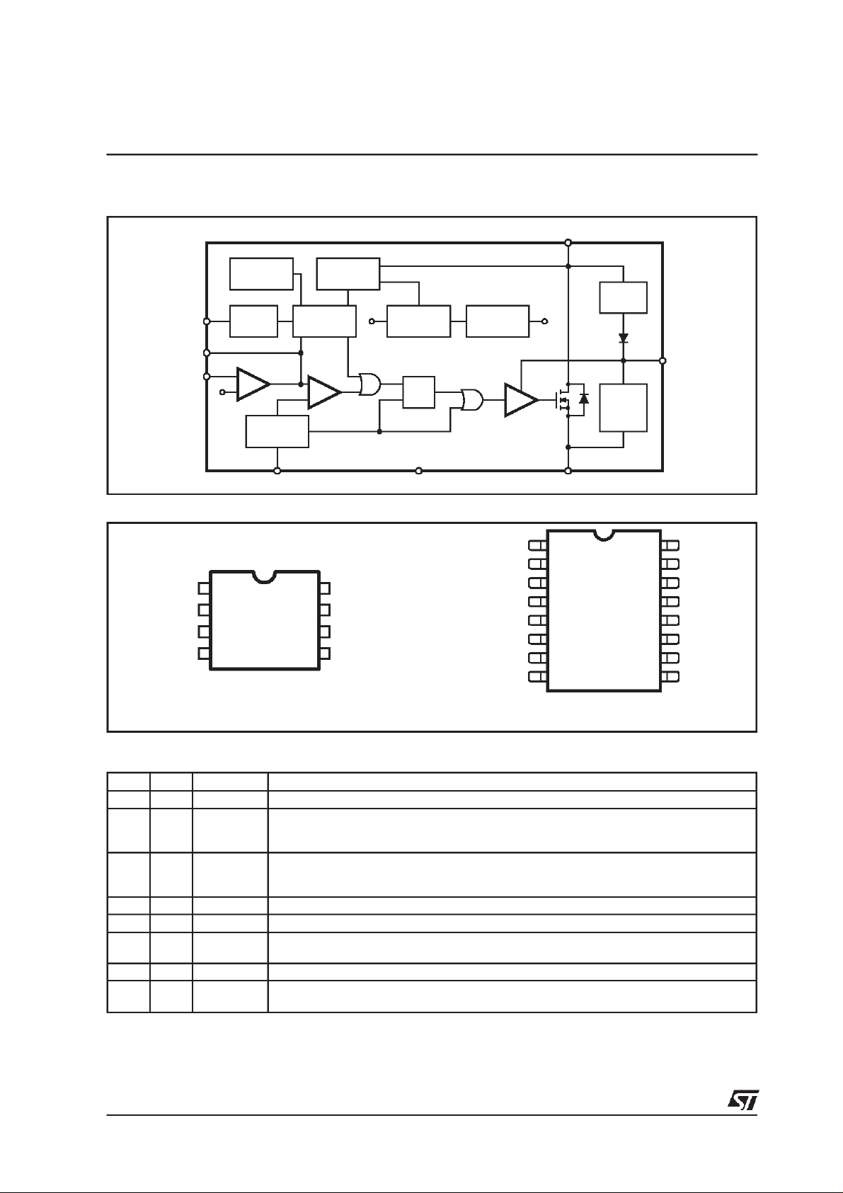
BLOCKDIAGRAM
COMP
FB
2
7
8
3.3V
SS_INH
THERMAL
SHUTDOWN
INHIBIT SOFTSTART
E/A
OSCILLATOR
VOLTAGES
MONITOR
PWM
3.3V
INTERNAL
REFERENCE
R
Q
S
INTERNAL
SUPPLY
5.1V
DRIVE
VCC
5
CBOOT
CHARGE
CBOOT
CHARGE
AT LIGHT
LOADS
6
BOOT
3
OSC GND OUT
1
4
D97IN594
PIN CONNECTIONS
GND
SS_INH
OSC
OUT
1
2
3
4 VCC
D97IN595
FB8
COMP
7
BOOT
6
5
Minidip
N.C.
GND
SS_INH
OSC
OUT
OUT
N.C.
N.C. N.C.
2
3
4
5
6
7
8
D97IN596
16
15
14
13
12
11
10
9
SO16W
N.C.1
N.C.
FB
COMP
BOOT
VCC
N.C.
PIN FUNCTIONS
DIP SO (*) Name Function
1 2 GND Ground
2 3 SS_INH A logic signal (active low) disables the device (sleep mode operation).
3 4 OSC An external resistor connected between the unregulated input voltage and this pin and
4 5, 6 OUT Stepdown regulator output
511 V
CC Unregulated DC input voltage
6 12 BOOT A capacitor connected between this pin and OUT allows to drive the internal DMOS
7 13 COMP E/A output to be used for frequency compensation
8 14 FB Stepdown feedback input. Connecting directly to this pin results in an output voltage of
(*) Pins 1, 7,8, 9, 10, 15 and 16 are not internally, electrically connected to the die.
A capacitor connected between this pin and ground determines the soft start time.
When this pin is grounded disables the device (driven by open collector/drain).
a capacitor connected from this pin to groundfix the switching frequency. (Linefeed
forward is automatically obtained)
Transistor
3.3V. An externalresistive divider is required for higher output voltages.
2/12

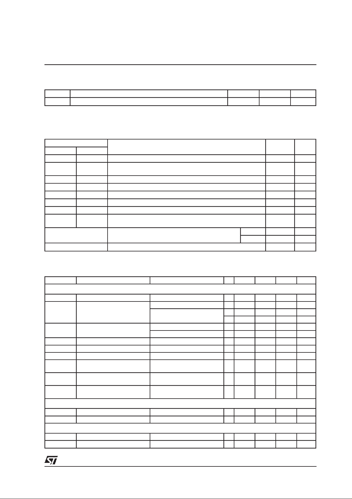
THERMALDATA
Symbol Parameter Minidip SO16 Unit
R
th(j-amb)
(*) Package mounted on board.
Thermal Resistance Junction to ambient Max. 90 (*) 110 (*) °C/W
ABSOLUTE MAXIMUM RATINGS
L4971
Symbol
Minidip S016
V
11
V5,V
I5,I
V12-V
V
12
V
13
V3 Analogs input voltage (VCC = 24V) 13 V
V
14
P
tot
V
V
5
V
4
I
4
6-V5
V
6
V
7
V
2
V
8
Input voltage 58 V
Output DC voltage
6
Output peak voltage at t = 0.1µs f=200KHz
Maximum output current int. limit.
6
11
Bootstrap voltage 70 V
Analogs input voltage (VCC= 24V) 12 V
(VCC= 20V) 6
Power dissipation a T
Parameter Value Unit
-1
-5
V
V
14 V
V
-0.3
≤ 60°C Minidip 1W
amb
V
SO16 0.8 W
T
j,Tstg
Junction and storage temperature -40 to 150 °C
ELECTRICAL CHARACTERISTICS (Tj = 25°C, Cosc = 2.7nF, Rosc = 20kΩ,VCC = 24V, unless other-
wisespecified.) * SpecificationReferedto Tj from 0 to 125°C
Symbol Parameter Test Condition Min. Typ. Max. Unit
DYNAMICCHARACTERISTIC
V
V
o
V
d Dropout voltage Vcc = 10V; Io = 1.5A 0.44 0.55 V
I
l Maximum limiting current Vcc = 8to 55V * 2 2.5 3 A
f
s Switching frequency * 90 100 110 KHz
SVRR Supply voltage ripple rejection V
Operating input voltage range Vo= 3.3 to 50V; Io= 1.5A * 8 55 V
I
Output voltage Io= 0.5A 3.33 3.36 3.39 V
I
= 0.2 to 1.5A 3.292 3.36 3.427 V
o
V
= 8to 55V * 3.22 3.36 3.5 V
cc
* 0.88 V
Efficiency V
Voltage stability of switching
o = 3.3V; Io = 1.5A 85 %
i =Vcc+2VRMS;Vo=Vref;
I
= 1.5A; f
o
ripple
= 100Hz
60 dB
Vcc = 8 to 55V 3 6 %
frequency
Temp. stability of switching
j = 0 to 125°C4%
T
frequency
Soft Start
Soft start charge current 30 40 50 µA
Soft start discharge current 6 10 14 µA
Inhibit
VLL Low level voltage * 0.9 V
I
sLL Isource Low level * 5 15 µA
3/12

L4971
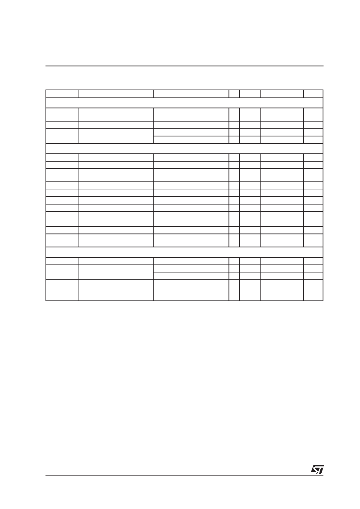
ELECTRICAL CHARACTERISTICS (continued)
Symbol Parameter Test Condition Min. Typ. Max. Unit
DC Characteristics
Iqop Total operating quiescent
current
I
q Quiescent current Duty Cycle = 0; V
I
qst-by
Total stand-by quiescent
current
V
<0.9V 100 200 µA
inh
Vcc = 55V; V
= 3.8V 2.5 3.5 mA
FB
<0.9V 150 300 µA
inh
Error Amplifier
V
FB
R
L Line regulation Vcc = 8 to 55V 5 10 mV
V
oH High level output voltage V
V
oL Low level output voltage V
I
o source Source output current V
I
o sink Sink output current V
I
b Source bias current 2 3 µA
SVRR E/A Supply voltage ripple rejection V
gm Transconductance I
Voltage Feedback Input 3.33 3.36 3.39 V
Ref. voltage stability vs
* 0.4 mV/°C
temperature
= 2.5V 10.3 V
FB
= 3.8V 0.65 V
FB
= 6V; VFB= 2.5V 200 300 µA
comp
= 6V; VFB= 3.8V 200 300 µA
comp
; Vcc = 8 to 55V 60 80 dB
= ∞ 50 57 dB
= -0.1 to 0.1mA
=6V
DC open loop gain R
comp=Vfb
L
comp
V
comp
OscillatorSection
Ramp Valley 0.78 0.85 0.92 V
Ramp peak Vcc= 8V 2 2.15 2.3 V
Vcc = 55V 9 9.6 10.2 V
Maximum duty cycle 95 97 %
Maximum Frequency Duty Cycle = 0%
R
osc
= 13kΩ,C
= 820pF
osc
46mA
2.5 ms
500 kHz
4/12
 Loading...