

L4969
SYSTEM VOLTAGE REGULATOR
WITH FAULT TOLERANT LOW SPEED CAN-TRANSCEIVER
PRELIMINARY DATA
■ OPERATING SU PPLY VOLTAGE 6V TO 28V,
TRANSIENT UP TO 40V
■ LOW QUIESCENT CURRENT CONSUMP-
TION, LESS THA N 40
■ TWO VERY LOW DROP VOLTAGE
REGULATORS 5V / 200mA
AND 5V/200mA
■ SEPARATE VOLTAGE REGULATOR FOR
CAN-TRANSCEIVER SUPPLY WITH LOW
POWER SLEEP MODE
■ EFFICIENT UC SUPERVISION AND RESET
LOGIC
■ 24 BIT SERIAL INTERF AC E
■ AN UNPOWERED OR INSUFFI C IENTLY
SUPPLIED NODE DOES NOT DIST U RB THE
BUS LINES
■ VS VOLTAGE SENSE COMPARATOR
■ SUPPORTS TRANSMISSION WITH
GROUNDSHIFT:
SINGLE WIRE: 1.5V, DIFFERENTIAL: 3V
µA IN SLEEP MODE
SO20 PowerSO20
ORDERING NUMBERS: L4969MD (SO20)
L4969 (PowerSO20)
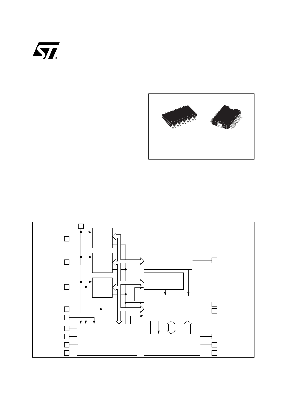
DESCRIPTION
The L4969 is an integrated circuit containing 3 independent Voltage Regulators and a standard fault tolerant low speed CAN line interface in multipower
BCD3S process.
It integrat es all mai n l ocal functions for automot iv e body
electronic applications conn ected to a CAN bus.
Figure 1. Block Diagram
VS
V1
V2
V3
RX
TX
CANH
RTH
CANL
RTL
VREG 1
VREG 2
VREG 3
Fault tole ran t
low speed
CAN-transceiver
Watchdo g and
adjustable RC-O s cillator
Iden tifier Filter
Control and Status Memory
24 Bit SPI
NRESET
WAKE
NINT
SCLK
SIN
SOUT
August 2003
This is preliminary information on a new product now in development or undergoing evaluation. Details are subject to change without notice.
1/35
L4969
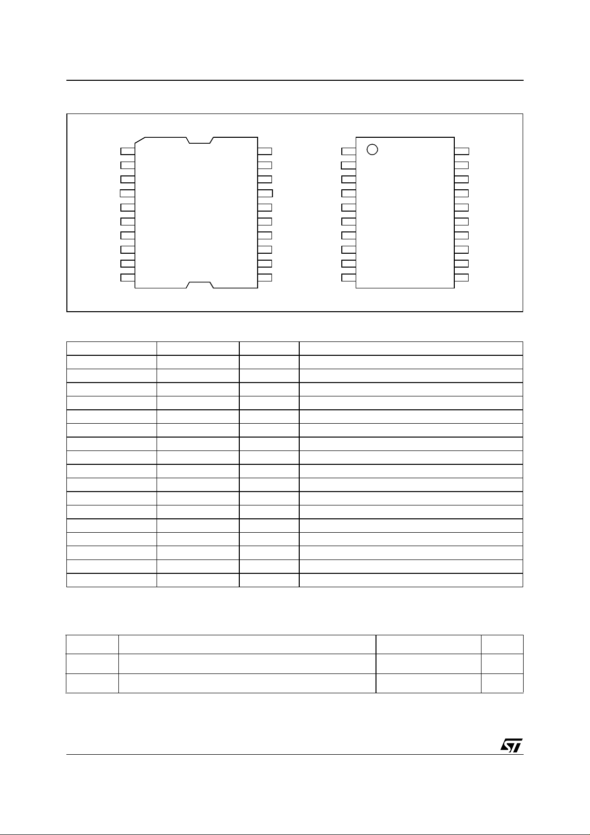
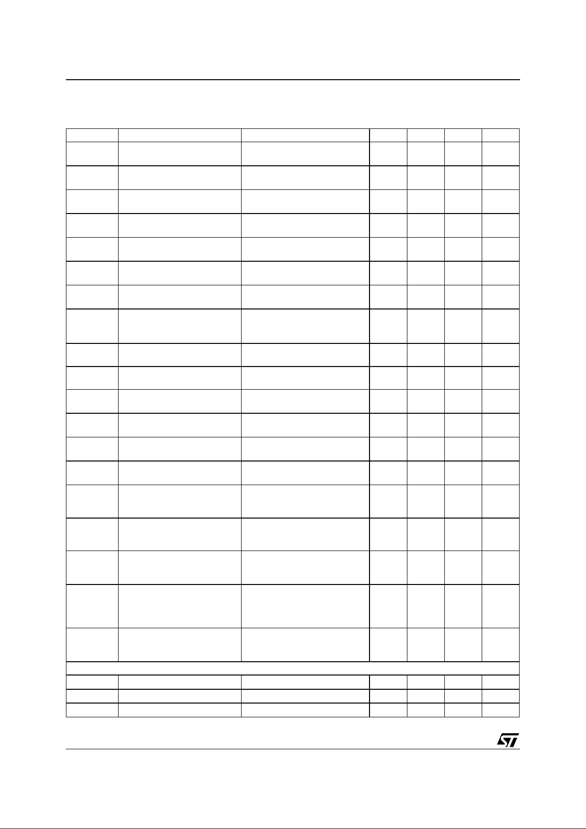
Figure 2. Pin Connection
GND
V1
V2
V3
VS
CANH
RTL
CANL
RTH
GND
Table 1.
Pin Functions
Pin No. (PSO20) Pin No. (SO20) Pin Name Function
1, 10, 11, 20 5,6, 15, 16 GND Power Ground
2 7 V1 Microcontroller Supply Voltage
3 8 V2 Peripheral Supply Voltage
4 9 V3 Internal CAN Supply
5 10 VS Power Supply
6 11 CANH CANH Line Driver Output
7 12 RTL CANL Termination Source
8 13 CANL CANL Line Driver Output
9 14 RTH CANH Termination Source
12 17 RXD Act. Low CAN Receive Dominant Data Output
13 18 TXD Act. Low CAN Transmit Dominant Data Input
14 19 SOUT Serial Data Output
15 20 SIN Serial Data Input
16 1 SCLK Serial Clock
17 2 NRES Act. Low Reset Output
18 3 NINT Act. Low Interrupt Request
19 4 WAKE Dual Edge Triggerable Wakeup Input
PSO20
GND
WAKE
NINT
NRES
SCLK
SIN
SOUT
TXD
RXD
GND
SCLK
NRES
NINT
WAKE
GND
GND
V1
V2
V3
VS
SO20
SIN
SOUT
TX
RX
GND
GND
RTH
CANL
RTL
CANH
Table 2. Thermal Data
Symbol Parameter Value Unit
R
thj-amb
R
thj-case
Note: 1. Typical value soldered on a PC board wit h 8 cm2 copper ground plane (35µm thick).
2/35
Thermal resistance junction-ambient
Thermal resistance junction-case 3 °C/W
40
1)
°C/W
Table 3. Absolute Maximum Ratings
Symbol Parameter Value Unit
V
VSDC
V
VSTR
I
VOUT1...3
T
STG
T
V
OUT1
V
OUT2
V
OUT3
V
inli
V
inliW
V
canh
V
canl
Notes: 1. All pins of the IC are protect ed against ESD. The verifi cation is perf ormed according to MIL 883C,
2. Voltage forced means voltage limited to the specified values whil e the current is not limited.
3. ESD Pulses on CAN-Pins up to 4K V HBM vs GND with all other P i ns grounded.
DC operating supply voltage -0.3 ... +28 V
Transient operating supply voltage (T < 400ms) -0.3 ... +40 V
Output currents Internally limited
Storage temperature -65 ... +150 T
Operating junction temperature -40 ... +150 T
J
Externally forced output voltage OUT1 -0.3 ... VS+0.3, max +6.3 V
Externally forced output voltage OUT2 -0.3 ... VS+0.3 V
Externally forced output voltage OUT3 -0.3 ... VS+0.3, max +6.3 V
Input voltage Logic inputs: SIN, SCLK, NRES -0.3 ... +7 V
Input voltage WAKE -0.3 ... VS+0.3 V
Voltage CANH line
Voltage CANL line
human body model with R = 1.5kW, C = 100pF and dischar ge voltage 200 0V,
corresponding to a maximum disch arge energy of 0.2mJ..
3
3
-28 ... +40 V
-28 ... +40 V
L4969
VSDC
VSTR
I
VOUT1...3
STG
J
OUT1
OUT2
OUT3
inli
inliW
canh
canl
Table 4. Electrical Characteristics
V
= 14V, Tj=-40°C to 150°C unless otherwise specified.
S
Symbol Parameter Test Conditions Min. Typ. Max. Unit
Supply Current
I
SSL
All Regulators off
(CANH Standby
I
SSLWK
V1 off, V2 off, V3 on
(CAN RX only)
I
SSB
I
S
V1 only (CAN Standby) Timer off (Standby #1) 150 250 µA
All Regulators on,
(CAN active, TX high)
I
SCP
Additional Oscillator- and
Chargepumpcurrent at low VS
Voltage Regulator 1
V
01
V
DP1
V1 output voltage 6V < VS < 28V
Dropout voltage 1@ VS=4.8V I
Timer off (Sleep #1) 30 40 60 µA
Timer on (Sleep #2) 70 90 135 µA
RXonly 4 6 mA
Timer on (Standby #2) 200 300 µA
Default (Standby #3) 440 600 µA
I
OUT1
I
OUT2
= -100mA
= -10mA
120 150 mA
No CAN load.
VS = 6V; Timer Off 55 80 100 µA
= 6V; Timer On 10 30 50 µA
V
S
4.9 5 5.1 V
IO >-100mA
SO20 Package
6V < V
I
>-150mA
O
< 28V
S
4.9 5 5.1 V
PSO20 Package
= -10mA 0.0 0.025 0.06 V
OUT1
I
OUT1
= -100mA
0.0 0.25 0.6 V
SO20 Package
I
OUT1
= -150mA
0.0 0.4 0.9 V
PSO20 Package
3/35
L4969
Table 4. Electrical Characteristics (continued)
V
= 14V, Tj=-40°C to 150°C unless otherwise specified.
S
Symbol Parameter Test Conditions Min. Typ. Max. Unit
V
OL01
I
LIM1
V
OLI1
T
OVT1
T
OTKL1
V
res
Voltage Regulator 2 and 3
V
O
V
DP
V
OLO
I
LIM
V
OLI
T
OVT
T
OTKL
Vtrc V2 tracking offset 6V < VS < 28V, I
Reset and Watchdog
t
OSC
t
WDC
t
RDnom
t
WDstart
Load regulation 1 IO =-1mA to-100mA
01040mV
SO20 Package
=-1mA to -150mA
I
O
01040mV
PSO20 Package
Current limit 1 0.8V < V
< 4.5V, VS=6V,
O1
-180 -400 -800 mA
SO20 Package
0.8V < V
O1
< 4.5V
-180 -400 -800 mA
VS=14V,
PSO20 Package
Line regulation 1 6V < VS < 28V
I
= -1mA
O1
0530mV
Overtemp flag 1 6V < VS < 28V 130 140 150 °C
Thermal shutdown 1 6V < VS < 28V 175 185 205 °C
Min V1 reset threshold voltage RTC0 = 0 4.15 4.5 4.7 V
RTC0 = 1 3.7 4.0 4.2 V
Output voltage 6V < VS < 28V
4.8 5 5.2 V
IO >-100mA
SO20 Package
6V < V
I
>-150mA
O
< 28V
S
4.8 5 5.2 V
PSO20 Package
Dropout voltage VS = 4.8V
= 100mA
I
O UT
0.0 0.25 0.6 V
SO20 Package
I
O UT
= 150mA
0.0 0.4 0.9 V
PSO20 Package
Load regulation IO =-1mA to -100mA
01040mV
SO20 Package
=-1mA to -150mA
I
O
01040mV
PSO20 Package
Current limit 0.8V < V
< 4.5V, VS=6V,
O1
-180 -400 -800 mA
SO20 Package
0.8V < V
O1
< 4.5V
-180 -400 -800 mA
PSO20 Package
Line regulation 6V < VS < 28V
I
= -5mA
OUT
0530mV
Overtemp flag 6V < VS < 28V 130 140 150 °C
Thermal shutdown 6V < VS < 28V 150 165 180 °C
= 0 -90 0 +90 mV
O2
OnChip RC-Timebase RC-Adjustment = 0 0.95 1.1 1.35 us
Watchdog timebase (2.5ms) 2498 t
Reset pulse duration (1ms) 1024 t
Reset pulse pause (320ms)
128 t
(startup watchdog)
OSC
OSC
WDC
4/35
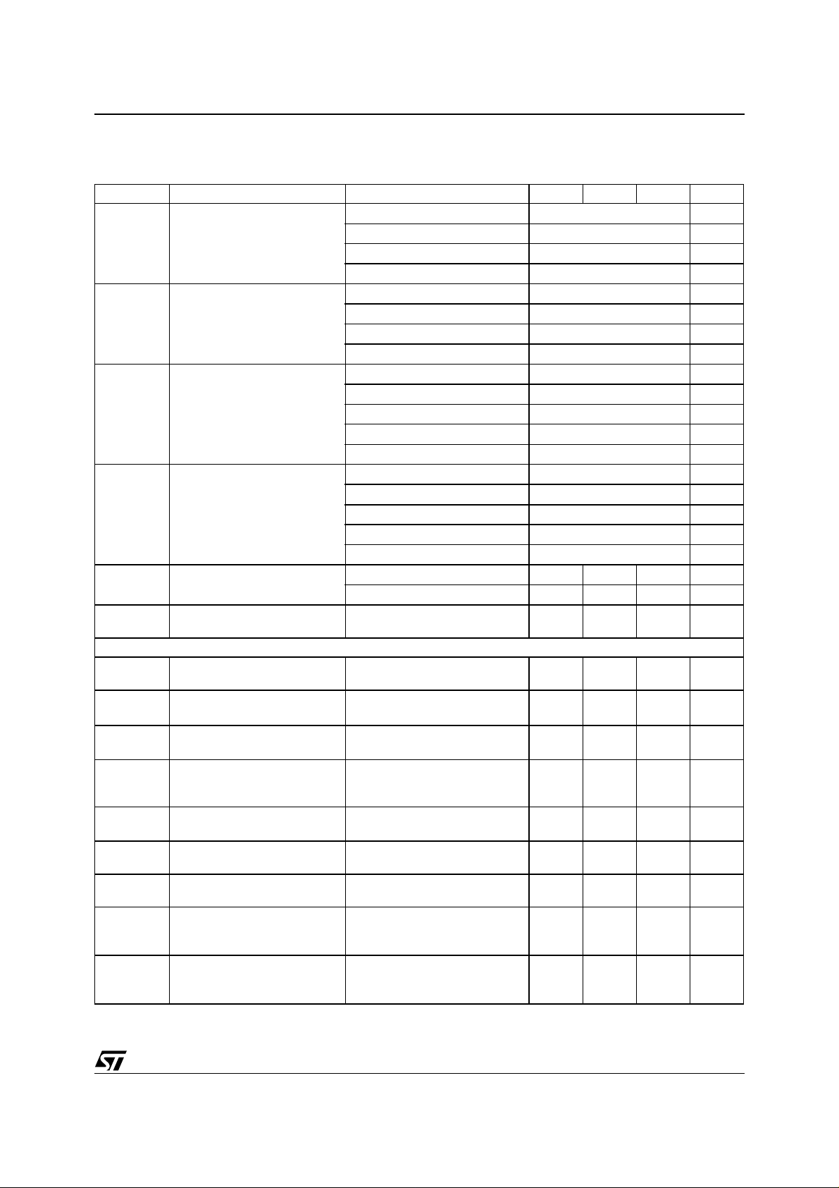
Table 4. Electrical Characteristics (continued)
V
= 14V, Tj=-40°C to 150°C unless otherwise specified.
S
Symbol Parameter Test Conditions Min. Typ. Max. Unit
t
WDswS
t
WDswE
t
WD1C
t
WD2C
V
RESL
R
PURES
CAN Line Interface
t
drd
t
ddr
S
RD
, R
R
RTH
V
CCFS
VH
RXD
VL
RXD
Vd_r Differential receiver
Vr_d Differential receiver
Watchdog window start
(Software window Watchdog)
SWT = 0 (2.5ms) 1 t
SWT = 1 (5ms) 2 t
SWT = 2 (10ms) 4 t
SWT = 3 (20ms) 8 t
Watchdog window end
(Software window watchdog)
SWT = 0 (5ms) 2 t
SWT = 1 (10ms) 4 t
SWT = 2 (20ms) 8 t
SWT = 3 (40ms) 16 t
System Watchdog 1 WDT = 0 (80ms) 32 t
WDT = 1 (160ms) 64 t
WDT = 2 (320ms) 128 t
WDT = 3 (640ms) 256 t
WDT = 4 (800ms) 320 t
System Watchdog 2 WDT = 8 (1s) 400 t
WDT = 9 (2s) 784 t
WDT = 10 (4s) 1600 t
WDT = 11 (8s) 3200 t
WDT = 12 (45min) 1081344 t
Reset output LOW voltage I
Internal Reset Pull-Up
= 500u, V1 = 2.5V 0 0.3 0.4 V
RES
= 500u, V1 = 1.5V 0 0.85 1.4 V
I
RES
80 120 280 KΩ
Resistance
Propagation delay
C
= 3.3n 0.4 1.0 1.5
load
(rec to dom state)
Propagation delay
(dom to rez state)
Bus output slew rate (r -> d) 10% ... 90%
external Termination
RTL
C
load
R
TERM
C
Load
= 3.3n,
=100
= 3.3n
0.4 1.0 2.0
458V/µs
0.5 16
resistance
(application limit)
Force Standby mode (fail
safe)
High level output voltage on
min VS to turn off CAN-IF and
V3
2.20 4.0 V
V1 - 0.9 V1 V
RXD
Low level output voltage on
0 0.9 V
RXD
No bus failures -3.85 -2.50 V
dom to rec threshold
- V
V
CANH
CANL
No bus failures -3.50 -2.20 V
rez to dom threshold
- V
V
CANH
CANL
L4969
WDC
WDC
WDC
WDC
WDC
WDC
WDC
WDC
WDC
WDC
WDC
WDC
WDC
WDC
WDC
WDC
WDC
WDC
µs
µs
Ω
K
5/35
L4969
Table 4. Electrical Characteristics (continued)
V
= 14V, Tj=-40°C to 150°C unless otherwise specified.
S
Symbol Parameter Test Conditions Min. Typ. Max. Unit
V
CANHr
V
CANHd
V
CANLr
V
CANLd
I
CANH
I
CANL
I
LCANH
I
LCANL
V
WakeH
V
WakeL
V
canhs
V
canls
V
OVH
V
OVL
RT
RTH
IT
RTHF
RT
RTL
IT
RTLF
RT
RTLS
Digital I/O
V
SINL
V
SINH
V
SCLKL
CANH recessive output
voltage
CANH dominant output
voltage
CANL recessive output
voltage
CANL dominant output
voltage
CANH dominant output
current
CANL dominant output
current
CANH Sleep mode
leakage current
CANL Sleep mode
leakage current
CANH wakeup voltage Sleep/
TXD = V1
< 4K
R
RTH
TXD = 0
= 40mA
I
CANH
TXD = V1
< 4K
R
RTL
TXD = 0
= -40mA
I
CANL
TXD = 0
= 0V
V
CANH
TXD = 0
= 14V
V
CANL
Sleep mode. Tj=150°C
= 0V
V
CANH
Sleep mode. Tj=150°C
= 0V
V
CANL
V
= 12V
S
V3 -
1.4V
V3 -
0.2V
70 100 160 mA
-70 -100 -160 mA
0
0
1.2 1.9 2.7 V
standby mode
CANL wakeup voltage Sleep/
2.4 3.1 3.8 V
standby mode
CANH single ended
receiver threshold
CANL single ended
receiver threshold
CANH overvoltage
detection threshold
CANL overvoltage
detection threshold
internal RTH to GND
Normal mode.
-5V < CANL < V
S
Normal mode.
-5V < CANH< V
S
Normal mode.
-5V < CANL < V
S
Normal mode.
-5V < CANH < V
= 1V 30 45 80 W
V
RTH
S
1.5 1.82 2.15 V
2.7 3.1 3.4 V
6.5 7.2 8.0 V
6.5 7.2 8.0 V
termination resistance
Normal mode, No failures.
internal RTH to GND
V
=V3 - 1V 55 75 100
RTH
termination current
Normal mode, Failure EIII
internal RTL to VCC
V
=V3 - 1V 30 45 85 W
RT L
termination resistance
Normal mode, no failures.
internal RTL to VCC
V
=V3 - 1V -6 -40 -70
RTL
termination current
Normal mode.
(failure EIV, EVI, EVII)
internal RTL to VS
termination resistance
Standby/sleep mode.
=1V, 4V
V
RTL
8 13.0 26
No failures.
Low level input voltage 0 0.9 V
High level input voltage V1 - 0.9 V1 V
Low level input voltage 0 0.9 V
0.35 V
1.4 V
µA
µA
µA
µA
K
V
V
Ω
6/35
Table 4. Electrical Characteristics (continued)
V
= 14V, Tj=-40°C to 150°C unless otherwise specified.
S
Symbol Parameter Test Conditions Min. Typ. Max. Unit
V
SCLKH
V
TXL
V
TXH
V
WakeL
V
WakeH
V
SoutH
V
SoutL
V
RXDH
V
RXDL
Ioh
RXD
Iol
RXD
Ioh
SOUT
Iol
SOUT
Ioh
Iol
INT
Ioh
Reset
Iol
Reset
Ioh
Wake
Iol
Wake
Serial Data Interface
t
Start
t
Setup
t
Hold
t
D
t
CKmax
t
GAP
f
SCLK
Diagnostic Functions
VS
min
GS
CANH
CAN Error Detection
N
EdgeH
N
EdgeHR
High level input voltage V1 - 0.9 V1 V
Low level input voltage 0 0.9 V
High level input voltage V1 - 0.9 V1 V
Low level input voltage 0 0.9 V
High level input voltage 4.1 5.0 V
High level output voltage V1 - 0.9 V1 V
Low level output voltage 0 0.9 V
High level output voltage V1 - 0.9 V1 V
Low level output voltage 0 0.9 V
High level output current RXD = 0 -1.2 -1.8 -2.5 mA
Low level output current RXD = 5V 1.1 1.6 2.2 mA
High level output current SOUT = 0 -9.0 -14.0 -18.0 mA
Low level output current SOUT = 5V 18.0 24,0 30.0 mA
High level output current INT = 0 -10.0 -15.0 -20.0 mA
INT
Low level output current INT = 5V 18,0 24,0 30,0 mA
High level output current RESET = 0 -6,0 -15,0 -25.0
Low level output current RESET = 5V 5.0 6.5 8.0 mA
High level output current V
Low level output current V
SIN low to SCLK low setup
= 5V 0 0 0.5
Wake
= 0V -2.2 -3.4 -4.5
Wake
100 ns
time
(frame start)
SIN to SCLK setup time
100 ns
(write)
SIN to SCLK hold time
100 ns
(write)
SCLK to SOUT delay time
(read)
SCLK maximum cycle time
1 1.5 3.0 ms
(timeout)
Interframe Gap 5 µs
SCLK frequency range 0.25 0.5 1 MHz
Sense comparator
6.0 7.2 8.0 V
detection threshold
CANH groundshift
-1.5 -1 -0.6 V
detection threshold
Nr of dom to rec edges on
Operating mode (EI_V) 3 Ed ges
CANL to detect permanent
rez CANH
Nr of dom to rec edges to
Operating mode (EI_V) 3 Ed ges
detect
recovery of CANH
500 ns
L4969
µA
µA
µA
7/35
L4969
Table 4. Electrical Characteristics (continued)
V
= 14V, Tj=-40°C to 150°C unless otherwise specified.
S
Symbol Parameter Test Conditions Min. Typ. Max. Unit
N
EdgeL
N
EdgeLR
t
EIII
t
EIIIR
t
EIV
t
EIVR
t
EVI
t
EVIR
t
EVII
t
EVIIR
t
EVIII
t
EVIIIR
t
FailTX
t
FailTXR
Wakeup
t
wuCAN
t
wuWK
Nr of dom to rec edges on
CANH to detect permanent
rez CANL
Nr of dom to rec edges to
detect
recovery of CANL
CANH to VS short circuit
detection time
CANH to VS short circuit
recovery time
CANL to GND short circuit
detection time
CANL to GND short circuit
recovery time
CANL to VS short circuit
detection time
CANL to VS short circuit
recovery time
CANL to CANH short circuit
detection time
CANL to CANH short circuit
recovery time
CANH to VDD short circuit
detection time
CANH to VDD short circuit
recovery time
TX permanent dominant
detection time (Fail safe)
TX permanent dominant
recovery time (Fail safe)
Minimum dominant time for
wake-up via CANH or CANL
Minimum pulse time for wakeup via WAKE
Operating mode (EII_IX) 3 Edges
Operating mode (EII_IX) 3 Edges
Operating mode (EIII) 1 .6 2 3.6 ms
Sleep/
1.6 2 3.6 ms
standby mode (EIII)
Operating mode (EIII) 0 .4 0.9 1.6
Sleep/
0.4 0.9 1.6
standby mode (EIII)
Operating mode (EIV) 0.4 0.9 1.6 ms
Sleep/
0.4 0.9 1.6 ms
standby mode (EIV)
Operating mode (EIV) 10 30 50
Sleep/
0.4 0.9 1.6
standby mode (EIV)
Operating mode (EVI) 0.4 0.9 1.6
Operating mode (EVI) 200 500 750
Operating mode (EVII) 0.4 0.9 1.6 ms
Operating mode (EVII) 10 30 50
Operating mode (EVIII) 1.6 1.8 3.6 ms
Sleep/
1.6 1.8 3.6 ms
standby mode (EVIII)
Operating mode (EVIII) 0.4 0.9 1.6 ms
Sleep/
0.4 0.9 1.6
standby mode (EVIII)
Operating mode (EX) 0.4 0.9 1.6 ms
Operating mode (EX) 1 4 8
sleep/standby 8 22 38
sleep/standby 8 22 38
ms
ms
µs
ms
ms
µs
µs
ms
µs
µs
µs
8/35
L4969
1 FUNCTIONAL DESCRIPTION
1.1 General Features
The L4969 is a monolithic integrated circuit which provides all main functions for an automotive body
CAN network.
It features two independent regulated v oltage supplies V1 and V2, an inter rupt and reset logic with internal cloc k
generator, Serial Interface and a low speed CAN-bus transceiver which is supplied by a separate third voltage
regulator (V3).
The device guarantees a clearly defined behavior in case of failure, to avoid permanent CAN bus errors.
The device operates in four basic modes, with additional programming for V1 Standbymodes in CTCR:
LP1, LP0
Mode V1 V2 V3 Timer/WDC CAN-IF
Sleep #1 Off Off Off Off Standby 40u x,x No Timer based wakeup
I
typ
(CTCR)
Remarks
Sleep #2 Off Off Off
(*1)
Standby #1
Standby #2
Standby #3 On Off Off On (1MHz) Standby 440u 0,0 Watchdog or timer activ, POR default
RXOnly Off Off On On (1MHz) RX-Only 4mA x,x Active during Busactivity to filter ID, auto-
Normal On On On On (1MHz) Normal 5mA x,x No Currents from CAN or Regulators
(*1) Note, that in order to enter either Standby #1 or Standby #2 the Startup-Watchdog has to be acknowledged (see Chapter 1.2), in Standby
#1, the Window Watchdog has to be disabled as described in Chapter 2.5, to allow the decativation of the internal oscillator.
On Off Off Off Standby 170u 1,1 No Watchdog or Timer
(*1)
On Off Off
On (250KHz)
On (250KHz)
Standby 80u x,x Timer active
Standby 210u 1,0 Watchdog or timer active
matic fall back to Sleep when Bus idle
1.1.1 V1 Output Voltage
The V1 regulator uses a DMOS transistor as an output stage. With this structure very low dropout voltage is
obtained. The dropout operation of the standby regulator is maintained down to 4V input supply voltage. The
output voltage is regulated up to the transient input supply voltage of 40V. With this feature no functional interruption due to overvoltage pulses is generated. The output 1 regulator is switched off in sleep mode.
1.1.2 V2 Output Voltage
The V2 regulator uses the same output structure as the output 1 regulator except to being short circuit proof to
VS, and to be rated for the output current of 200mA. The V2 output can be switched on and off through a dedicated enable bit in the control register. In addition a tracking option can be enabled to allow V2 follow V1 with
constant offset. This feature allows c onsistent A /D conver sion insi de the
µ
C (supplied by V 1) when the converted signals are referenced to V2. The maximum voltage that can be applied to V2 is VS + 0.3V up to a max VS
of 40V.
1.1.3 V3 Output Voltage
The third voltage regulator of the device generates the supply voltage for the internal logic and the CAN-transceiver. In operating mode it is capable of supplyi ng up to 200mA in order to guarantee the required short ci rcuit
current for the CAN_H driver. The sleep and operating modes are switched through a dedicated enable bit.
1.1.4 Internal Supply Voltage
A low power sleep mode regulator supplies the internal logic in sleep mode.
9/35
L4969
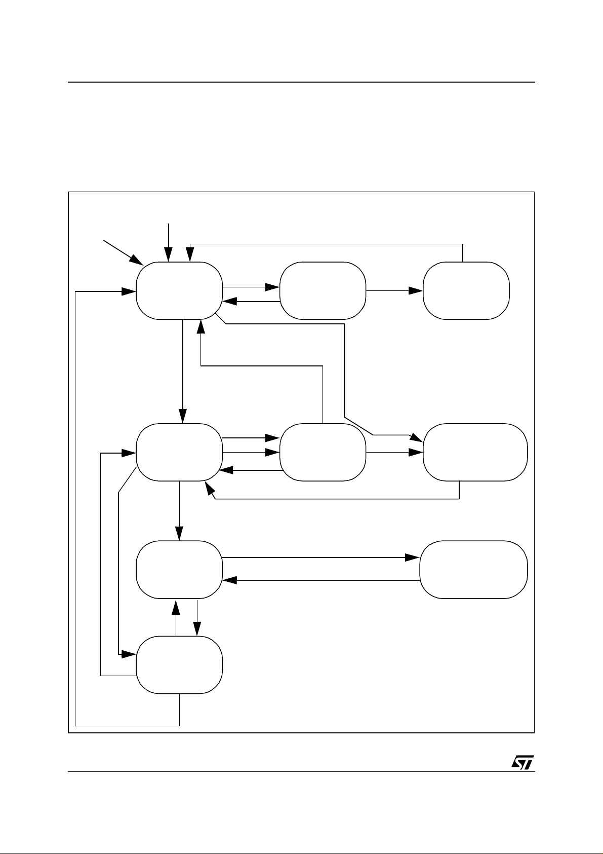
1.2 Power-Up, Initialization and Sleep mod e transitions
The following state-diagram illustrates the possible mode transitions inside the device.
As a prerequisite, a SPI-connection to the uC with the correct CRC-algorythms is required.
During the debug phase the NRES line can be forced high externally (connect to V1) to deactivate the startup
failure mechanis keeping V1 will alive.
Figure 3.
After POR, V1 up or externally forced reset
through low NRES, the STARTUP STATE is
entered
V1 Low
NRES Low
WAKEUP
STARTUP
V1 active
V2, V3, CAN off
WDC-ACK
Dependi g on th e value f rom the last
WDC-ACK, another one has to be
Writing to the WDCregister (WDC-ACK)
the NORMAL STATE is
entered.
written within the spec ified time frame
(SWDC[1:0]). A failure will activate
the STARTUP STATE
NORMAL MODE
WINDOW WDC
ACTIVE
WND SET
DISAR
SET
If during the last WDC-ACK WND has been set (after releasing
write lock , see d escription of Watc hdog Cont rol Register) th e Window wa tch do g is de act ivat e d, an d no uC sup erv ision is active.
NORMAL MODE
WINDOW WDC
DISABLED
The forced sleep mode is left upon wakeup through either CAN or edge on
WAKE. Appl ying a per manent wakeup ( i. e. bot h CAN-l ines domin ant) pr events V1 from being turned off (can be used during System debugging)
WAKEUP
Forcing NRES high externally, fail will not be incremented (Emulation)
STARTUP
t=320ms
FAILURE
fail = 7
RESET low
t=1ms
A missing ACK within 320ms will
initiate a STARTUP FAILURE
phase (RESET low).
WDC-FAIL
(fail ++)
If no WDC-ACK is recei ved within
seven retrials the voltage regulator
WDC-ACK
&
WDEN SET
The Window supervision can temporarily be deactivated for the time programmed during the
last WDC-ACK (WDT[3:0]). Upon rewriting
(WDC -AC K) or e xpiry of the time r, the NO R MAL
STATE is reentered.
V1 will be turned off by entering the
FORCED SLEEP state.
WDC-ACK
t=t
WIN2
WDC-OK
WINDOW
WATCHDOG
REFRESH
TIMEOUT | WDC-ACK
WDEN SET
TIMEOUT | WDC-ACK
FORCED SLEEP
V1 off
No Reset
TIMER
ACTIVEWDEN SET
(restart by double
WDC-ACK & WDEN)
Here the t imer ca n b e used to
generate time events (i.e.
wakeup uC from stop)
TIMER
ACTIVE
(restart by double
WDC-ACK & WDEN)
WAKEUP
&V1_UV
WAKEUP&V1_UV
10/35
WAKEUP
Programmed
SLEEP
V1 OFF
No Reset
DISAR
SET
Setti ng DI SAR ( see V ol t age Reg ul a t or Con t r ol R egi s te r ) Vol t ag e r e gu la t or V1 i s
turned off, and the output voltage is decreasing depending on the external load
and blocking capa citor .
Note, that during this transition no Reset will be generated (due to Debugmode).
Upon wakeup howewer NRES wil l be pulled low, if V1was below the programmable reset threshold (V1_UV).
L4969
1.3 CAN Transceiver
– Supports double wire unshielded busses
– Baud rate up to 125KBaud
– Short circuit protection (battery, ground, wires shorted)
– Single wire operation possible (automatic switching to single wire upon bus failures)
– Bus not loaded in case of unpowered transceiver
The CAN transceiver stage is able to transfer serial data on two independent communication wires either deferentially (n ormal operation) or in case of a single wi re fault on the remaining li ne. The physical bitcoding is done
using dominant (transmitter active) and overwritable recessive states. Too long dominant phases are detected
internally and further transmission is automatically disabled (malfunction of protocol unit does not affect communication on the bus, "fail-sa fe" - mechanism). For low current consu mption during bus inactiv ity a sleep mode
is available. The operating mode can be entered from the sleep mode either by local wake up (
tection of a dominant bit on the CAN-bus (external wake up).
Ten different errors on the physical buslines can be distinguished:
1.3.1 Detectable Physical Busline Failures
N Type of Errors Conditions
Errors caused by damage of the datalines or isolation
µ
C) or upon de-
I CANH wire interrupted (tied to Ground or termination) Edgecount difference > 3
II CANL wire interrupted (floating or tied termination) Edgecount difference > 3
III CANH short circuit to V
IV CANL short circuit to GND (permanently dominant) V(CANL) < 3.1V & V(CANH)-V(CANL)
V CANH short circuit to GND (permanently recessive) Edgecount difference > 3
VI CANL short circuit to V
VII CANL shorted to CANH V(CANH) - V(CANL) < -3.25V after
Errors caused by misbehavior of transceiver stage
VIII CANH short circuit to VDD (permanently dominant) V(CANH) > 1.8V & V(CANH) -
IX CANL short circuit to VDD (permanently recessive) Edgecount difference > 3
Errors caused by defective protocol unit
X CANH, CANL driven dominant for more than 1.3ms
(overvoltage condition) V(CANH) > 7.2V after 32us
BAT
< -3.25V after 1.3ms
(overvoltage condition) V(CANL) > 7.2V after 32us
BAT
1.3ms
V(CANL) < -3.25V after 2.5ms
Not all of the 10 different errors lead to a breakdown of the whole communication.
So the errors can be categorized into 'negligible', 'problematic' and 'severe':
11/35
 Loading...