

HIGHCURRENT SWITCHING REGULATOR
.4 AOUTPUTCURRENT
.5.1 V TO28 V OUTPUTVOLTAGERANGE
.0 TO 100 % DUTY CYCLERANGE
.PRECISE(± 3 %) ON-CHIPREFERENCE
.SWITCHINGFREQUENCY UP TO 120KHz
.VERYHIGH EFFICIENCY(UP TO 90 %)
.VERYFEW EXTERNALCOMPONENTS
.SOFTSTART
.RESETOUTPUT
.CURRENT LIMITING
.INPUT FOR REMOTE INHIBIT AND SYN-
CHRONUSPWM
.THERMALSHUTDOWN
DESCRIPTION
TheL4964isa stepdownpowerswitchingregulator
delivering4Aat a voltagevariablefrom5.1Vto28V.
Featuresof the device includeoverloadprotection,
soft start,remote inhibit,thermal protection,a reset
outputformicroprocessorsanda PWMcomparator
inputforsynchronizationinmultichipconfigurations.
TheL4964ismountedina 15-leadMultiwatt plas-
tic power package and requires very few external
components.
Efficient operation at switching frequencies up to
120kHzallowsareductionin thesizeandcostofexternalfilter components.
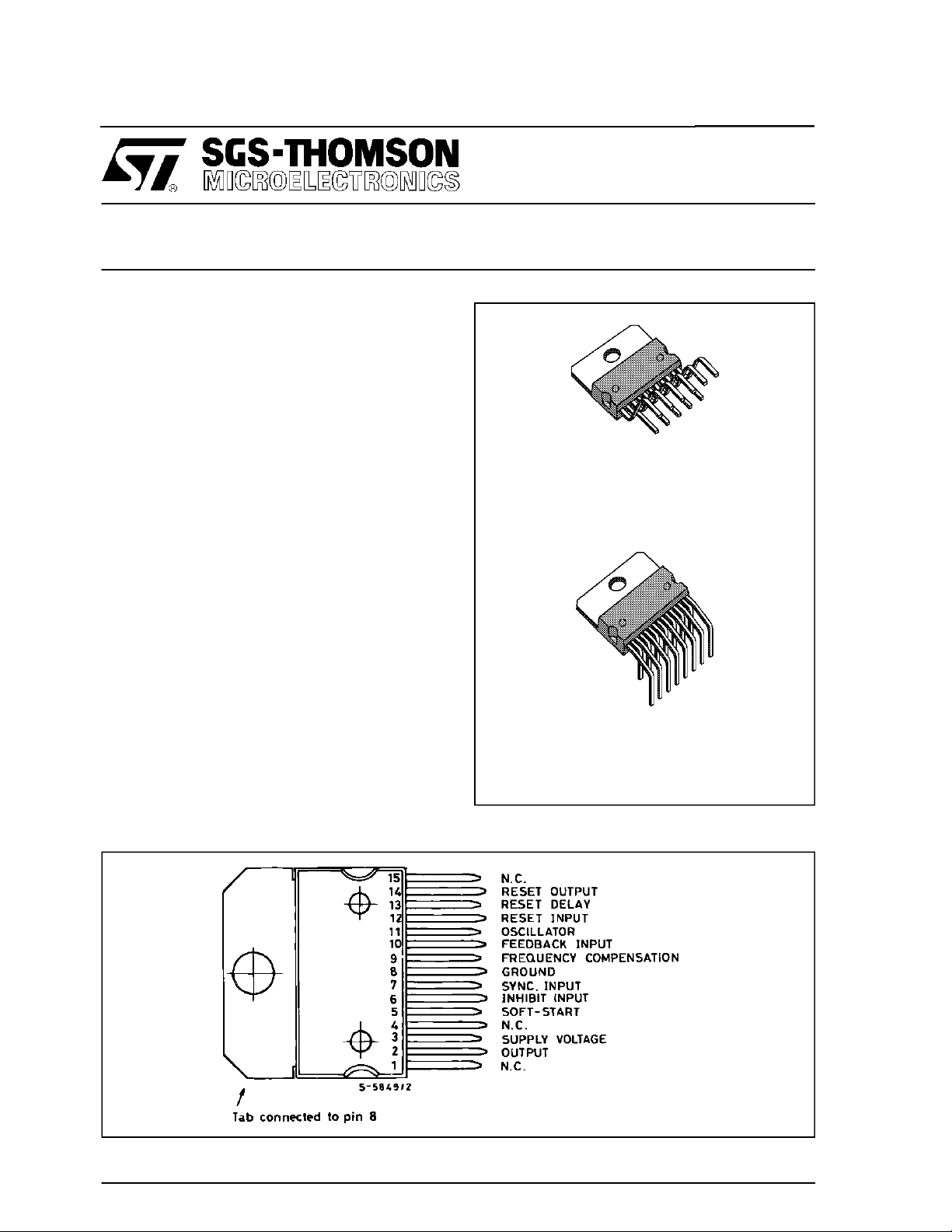
L4964
MULTIWATT15 Vertical
(PlasticPackage)
ORDERING NUMBER : L4964
MULTIWATT15 Horizontal
(PlasticPackage)
ORDERING NUMBER : L4964HT
PIN CONNECTION (top view)
April1993
Pins1, 4, 15 must not be connected. Leave open circuit.
1/13
L4964
PIN FUNCTIONS
N° Name Function
1 N.C. Must not be connected. Leave open circuit.
2 Output Regulator Output.
3 Supply Voltage Unregulated Voltage Input. An internal regulator powers the L4964’s internal logic.
4 N.C. Must not be connected. Leave open circuit.
5 Soft Start Soft Start Time Constant. A capacitor is connected between this terminal and ground
6 Inhibit Input TTL - Level Remote Inhibit. A logic high level on this input disables the L4964.
7 Sync Input Multiple L4964’s are synchronized by connecting the pin 7 inputs together and omitting
8 Ground Common Ground Terminal.
9 Frequency
Compensation
10 Feedback
Input
11 Oscillator A parallel RC network connected to this terminal determines the switching frequency.
12 Reset Input Input of the Reset Circuit. The threshold is roughly 5 V. It may be connected to the
13 Reset Delay A capacitorconnected between this terminal and ground determines the reset signal
14 Reset Output Open Collector Reset Signal Output. This output is high when the supply is safe.
15 N.C. Must not be connected. Leave open circuit.
to define the soft start time constant. This capacitor also determines the average short
circuit output current.
the oscillator RC network on all but one device.
A series RC network connected between this terminal and ground determines the
regulation loop gain characteristics.
The FeedbackTerminal of the Regulation Loop. The output is connected directly to
this terminal for 5.1 V operation ; it is connected via a divider for higher voltages.
The pin must be connected to pin 7 input when the internal oscillator is used.
beedback point or via a divider to the input.
delay time.
BLOCK DIAGRAM
2/13
CIRCUI T OPE RATION (refer t o the bl ock diagram)
TheL4964isa monolithicstepdownswitchingregu-
lator providing output voltages from 5.1 V to 28 V
anddelivering 4A.
Theregulationloopconsistsofasawtoothoscillator,
erroramplifier,comparatorandtheoutputstage.An
error signal is produced by comparing the output
voltage with a precise 5.1 V on-chip reference
(zener zap trimmed to ± 3 %). This error signal is
thencomparedwiththesawtoothsignaltogenerate
the fixed frequency pulse width modulated pulses
which drive the output stage. The gain and frequencystabilityoftheloop canbeajustedbyan externalRC networkconnectedto pin 9. Closing the
loopdirectlygivesanoutputvoltageof5.1V.Higher
voltagesareobtainedby insertinga voltagedivider.
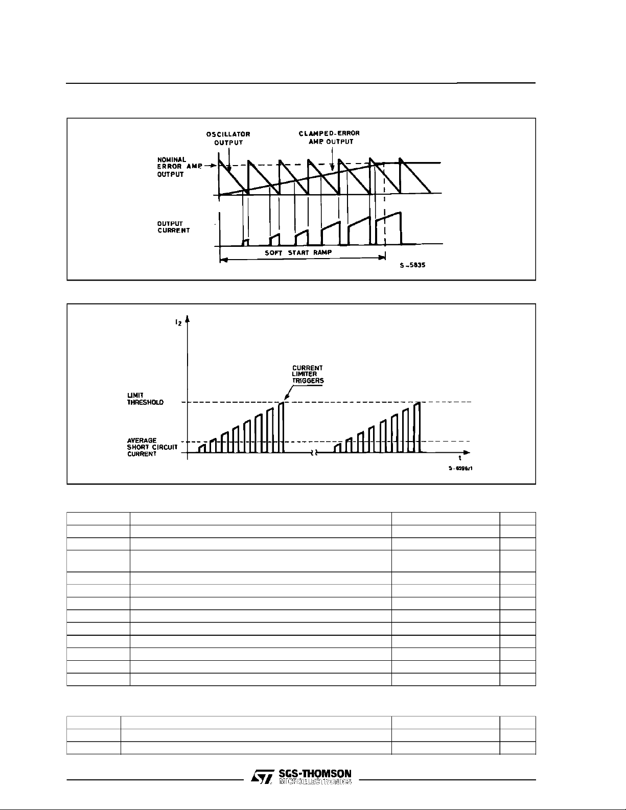
Outputovercurrentsat switch on are preventedby
the soft start function.The error amplifieroutput is
initiallyclampedbytheexternalcapacitorC
andal-
ss
lowedto rise, linearly,as this capacitoris charged
bya constantcurrent source.
Outputoverloadprotectionisprovidedinthe formof
a current limiter. The load current is sensedby an
internalmetal resistor connectedto a comparator.
Whenthe load current exceedsa presetthreshold
this comparatorsets a flip flop which disables the
outputstageanddischargesthesoftstartcapacitor.
A second comparator resets the flip flop when the
voltageacross the soft start capacitorhas fallento
0.4 V. The output stage is thus re-enable and the
outputvoltagerisesundercontroofthesoftstartnetwork. If the overload condition is still present the
limiter will trigger againwhen the thersholdcurrent
isreached.The averageshortcircuit current is limitedto a safe value by the dead timeintroducedby
the soft start network.
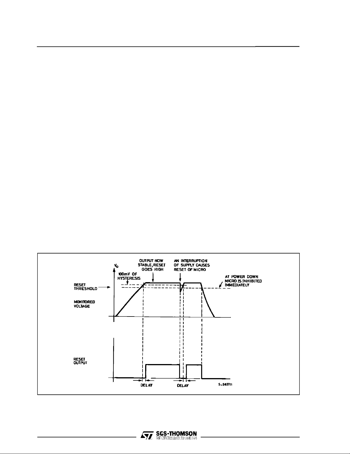
The reset circuit generates an output signal when
the supply voltage exceeds a threshold programmedbyan externaldivider.The resetsignal is
generatedwithadelaytimeprogrammedby an external capacitor. When the supply falls below the
threshold the reset output goes low immediately.
Thereset output is an opencollector.
A TTL- level input is providedfor applicationssuch
as remote on/off control.This input is activated by
highlevelanddisablescircuitoperation.Afteran inhibittheL4964restartsundercontrolofthesoftstart
network.
The thermal overloadcircuit disables circuit operation when the junction temperaturereaches about
150 and has hysteresisto prevent unstable conditions.
L4964
Figure 1 : ResetOutputWaveforms
3/13
L4964
Figure 2 : SoftStartWaveforms
Figure 3 : CurrentLimiterWaveforms
ABSOLUTE MAXIMUM RATINGS
Symbol Parameter Value Unit
V
i
V
i–V2
V
2
V
12
V
5,V7,V9
V
10,V6,V13
V
14
I
9
I
11
I
14
P
tot
T
,T
j
Input Voltage (pin 3) 36 V
Input to Output Voltage Difference 38 V
Output DC Voltage
Output Peak Voltage at t = 0.1 µsec f = 100 kHz
–1
–7
Voltage at Pin 12 10 V
Voltage at Pins 5, 7 and 9 5.5 V
Voltage at Pins 10, 6 and 13 7 V
Voltage at Pin 14 (I14≤ 1 mA) V
i
Pin 9 Sink Current 1 mA
Pin 11 Source Current 20 mA
Pin 14 Sink Current (V14< 5 V) 50 mA
Power Dissipation at T
Junction and Storage Temperature – 40 to 150 °C
stg
≤ 90 °C20W
case
THERMAL DATA
Symbol Parameter Value Unit
4/13
R
th j-case
R
th j-amb
Thermal Resistance Junction-case Max. 3 °C/W
Thermal Resistance Junction-ambient Max. 35 °C/W
V
V
 Loading...