

L4957
UP TO 4A ULDO LINEAR REGULATOR
1.5V AND 2.5VFIXEDOUTPUT VOLTAGE
3V TO 6.5V INPUTVOLTAGERANGE
200mΩ RdsonTYPICAL @ T
j = 125°C
0.6V max. DROP-OUTAT 2A
EXCELLENTLOAD REGULATION
0.6mAQUIESCENTCURRENTAT ANYLOAD
SHORT CIRCUIT PROTECTIONWITH FOLD-
BACK
THERMALSHUTDOWN
APPLICATIONS
MOTHERBOARDS
PROCESSORI/O & SUPPLIES
LOW VOLTAGE MEMORY & CHIP SET SUP-
PLIES
GRAPHIC& SOUND CARDS
LOW VOLTAGELOGIC SUPPLIES
POSTREGULATOR FOR SMPS
DESCRIPTION
The L4957 devicesare Ultra LowDrop Output linear regulators with an internal N-channel MOS of
200mΩ particulary suitable for low voltage/low
dropout applications.
Operating with a input voltage from 3V to 6.5V
they are capable to deliver up to 4A at 1.5V or
2.5V fixed output voltages.
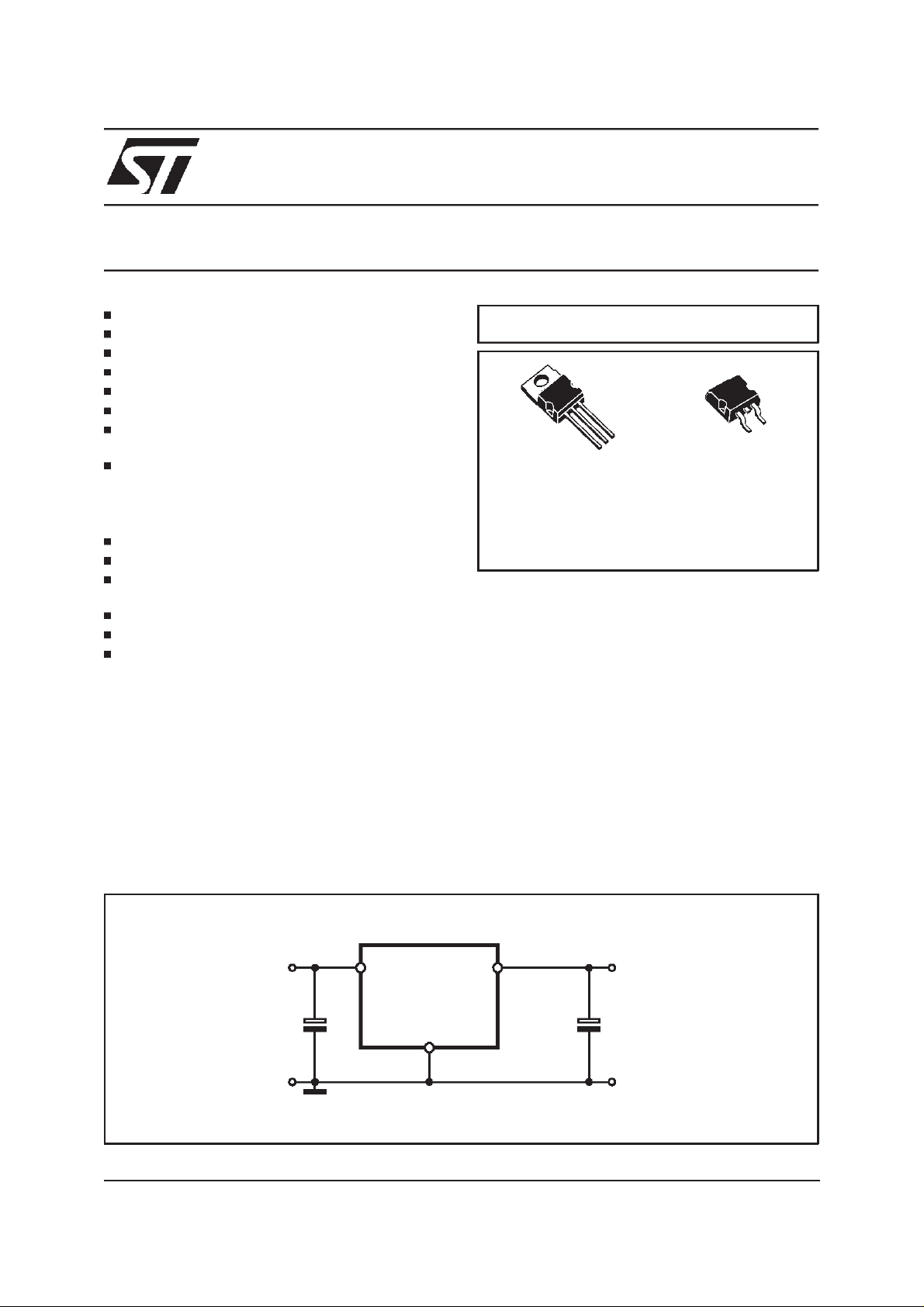
MULTIPOWER BCD TECHNOLOGY
3
1
D2PAKVersawatt TO-220
ORDERING NUMBERS:
L4957V1.5 L4957D1.5
L4957V2.5 L4957D2.5
The devices are ideal for use as one of the supplies required by processor, for example they are
the cost effectiveand efficientsolution for conversion from 3.3V (rail bus) to 2.5V @ 2.5A or to
1.5V with high current rating.
Fast response transient minimise the output ca-
pacitor value. A minimum of 22µF assures the
stabilityin allload conditions.
The on-chip trimming technique offers a tighter
voltage reference tolerance (with ±
2% including
line and load variation) beside to ensure a controlled short circuit current. Thermal shutdown
provides protection against overload conditions
that createsexcessivejunction temperature.
TYPICALAPPLICATION
3V to 6.5V
February 2000
C1
V
=1.5V/2.5V
OUTIN
1
3
OUT
L4957
2
GND
D97IN657E
C2
1/7
L4957
ABSOLUTE MAXIMUM RATINGS
Symbol Parameter Value Unit
V
IN
T
i
T
stg
PINS CONNECTION
Supply Input Voltage 7 V
Junction Temperature -40 to +150 °C
Storage Temperature -40 to +150 °C
Versawatt (TO220)
BLOCK DIAGRAM
V
IN
10µF
IN
1
3
2
1
D98IN838B
OUT
GND
IN
3
2
GND
1
OUT
IN
D98IN933A
D2PAK
CURRENT
V
REF
LIMIT
WITH
FOLDBACK
CHARGE
PUMP
2/7
PRE
REGULATOR
+
E/A
-
BUFFER
THERMAL
SHUTDOWN
GND
2
POWER
DMOS
150mΩ
R
X
R
Y
3
OUT
D98IN839C
V
22µF
OUT
PIN FUNCTIONS
Pin N° Name Function
1 IN Unregulated input voltage; this pin mustbe bypassed with a capacitor larger than 10µF.
2 GND To connect to Ground to get 1.5V or2.5V output.
3 OUT Regulated output voltage. A minimum bypass capacitor of 22µF is required to insurestability.
THERMAL DATA
Symbol Parameter TO220 D2PAK Unit
R
th j-case
R
th j-amb
Thermal ResistanceJunction-case Max. 2.5 3 °C/W
Thermal ResistanceJunction-ambient Max. 50 60 °C/W
Thermal Shutdown Typ. 150 °C
Thermal Hysteresis Typ. 20 °C
L4957 - ELECTRICALCHARACTERISTICS (Tj=25°C, VIN=5V, unlessotherwise specified).
• =Specificationsreferred to T
Symbol Parameter Test Condition Min. Typ. Max. Unit
V
IN
V
O
V
∆
DSON Drain-Source ON
R
I
O
I
Q
(1) GND connected to ground.
OperatingSupply Voltage
(1)
Output Voltage (1) ForL4957V1.5/D1.5
Load regulation (1) 0.1A < IO < 4A 2 10 mV
O
Resistance
Current Limiting 90% V
Short Circuit Current V
Quiescent Current 0.1A < IO<4A 3V<V
Ripple Rejection f = 120Hz,I
from0°Cto +125°C.
J
0.1A< I
3V < V
<4A; 3V< VIN<6.5V
O
<6.5V; 0.1A< I
IN
ForL4957V2.5/D2.5
0.1A< I
3V < V
O
V
IN
<4A; 3V< VIN<6.5V
O
<6.5V; 0.1A< IO<4A
IN
O
=0V • 1.8 A
O
=5V∆VIN=2V
=4A
3 6.5 V
<4A •
O
•
1.47
1.455
2.45
2.425
1.5
1.5
2.5
2.5
1.53
1.545
2.55
2.575
• 200 300 m
5.1 6.3 7.5 A
•
< 6.5V • 0.5 2 mA
IN
60 75 dB
PP
L4957
V
V
V
V
Ω
Figure 1: Line Regulation vs. Junction
Temperature
5
4.5
4
3.5
3
2.5
2
Output Voltage Deviation [mV]
1.5
1
0.5
0
-40 -20 0 20 40 60 80 100 120 140 160
3V < Vin < 6.5V
Iout = 10mA
Tj [°C]
Figure2: LoadRegulation
5
4
3
2
1
0
Output VoltageDeviation [mV]
-1
-2
-3
-4
-5
012345
(Pulsed technique has been used)
Vin = 5V
Tj = 25 °C
Vout = 1.5V
Iout [A]
3/7
 Loading...