

L4957
UP TO 4A ULDO LINEAR REGULATOR
1.5V AND 2.5VFIXEDOUTPUT VOLTAGE
3V TO 6.5V INPUTVOLTAGERANGE
200mΩ RdsonTYPICAL @ T
j = 125°C
0.6V max. DROP-OUTAT 2A
EXCELLENTLOAD REGULATION
0.6mAQUIESCENTCURRENTAT ANYLOAD
SHORT CIRCUIT PROTECTIONWITH FOLD-
BACK
THERMALSHUTDOWN
APPLICATIONS
MOTHERBOARDS
PROCESSORI/O & SUPPLIES
LOW VOLTAGE MEMORY & CHIP SET SUP-
PLIES
GRAPHIC& SOUND CARDS
LOW VOLTAGELOGIC SUPPLIES
POSTREGULATOR FOR SMPS
DESCRIPTION
The L4957 devicesare Ultra LowDrop Output linear regulators with an internal N-channel MOS of
200mΩ particulary suitable for low voltage/low
dropout applications.
Operating with a input voltage from 3V to 6.5V
they are capable to deliver up to 4A at 1.5V or
2.5V fixed output voltages.
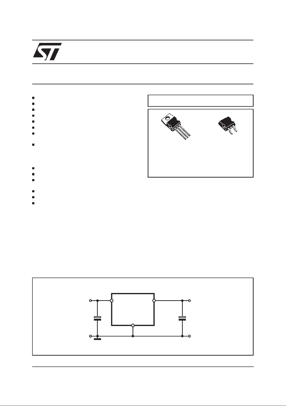
MULTIPOWER BCD TECHNOLOGY
3
1
D2PAKVersawatt TO-220
ORDERING NUMBERS:
L4957V1.5 L4957D1.5
L4957V2.5 L4957D2.5
The devices are ideal for use as one of the supplies required by processor, for example they are
the cost effectiveand efficientsolution for conversion from 3.3V (rail bus) to 2.5V @ 2.5A or to
1.5V with high current rating.
Fast response transient minimise the output ca-
pacitor value. A minimum of 22µF assures the
stabilityin allload conditions.
The on-chip trimming technique offers a tighter
voltage reference tolerance (with ±
2% including
line and load variation) beside to ensure a controlled short circuit current. Thermal shutdown
provides protection against overload conditions
that createsexcessivejunction temperature.
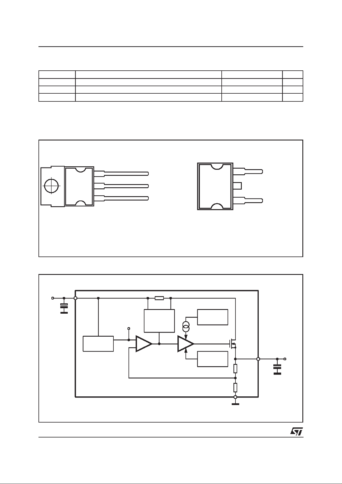
TYPICALAPPLICATION
3V to 6.5V
February 2000
C1
V
=1.5V/2.5V
OUTIN
1
3
OUT
L4957
2
GND
D97IN657E
C2
1/7
L4957
ABSOLUTE MAXIMUM RATINGS
Symbol Parameter Value Unit
V
IN
T
i
T
stg
PINS CONNECTION
Supply Input Voltage 7 V
Junction Temperature -40 to +150 °C
Storage Temperature -40 to +150 °C
Versawatt (TO220)
BLOCK DIAGRAM
V
IN
10µF
IN
1
3
2
1
D98IN838B
OUT
GND
IN
3
2
GND
1
OUT
IN
D98IN933A
D2PAK
CURRENT
V
REF
LIMIT
WITH
FOLDBACK
CHARGE
PUMP
2/7
PRE
REGULATOR
+
E/A
-
BUFFER
THERMAL
SHUTDOWN
GND
2
POWER
DMOS
150mΩ
R
X
R
Y
3
OUT
D98IN839C
V
22µF
OUT
PIN FUNCTIONS
Pin N° Name Function
1 IN Unregulated input voltage; this pin mustbe bypassed with a capacitor larger than 10µF.
2 GND To connect to Ground to get 1.5V or2.5V output.
3 OUT Regulated output voltage. A minimum bypass capacitor of 22µF is required to insurestability.
THERMAL DATA
Symbol Parameter TO220 D2PAK Unit
R
th j-case
R
th j-amb
Thermal ResistanceJunction-case Max. 2.5 3 °C/W
Thermal ResistanceJunction-ambient Max. 50 60 °C/W
Thermal Shutdown Typ. 150 °C
Thermal Hysteresis Typ. 20 °C
L4957 - ELECTRICALCHARACTERISTICS (Tj=25°C, VIN=5V, unlessotherwise specified).
• =Specificationsreferred to T
Symbol Parameter Test Condition Min. Typ. Max. Unit
V
IN
V
O
V
∆
DSON Drain-Source ON
R
I
O
I
Q
(1) GND connected to ground.
OperatingSupply Voltage
(1)
Output Voltage (1) ForL4957V1.5/D1.5
Load regulation (1) 0.1A < IO < 4A 2 10 mV
O
Resistance
Current Limiting 90% V
Short Circuit Current V
Quiescent Current 0.1A < IO<4A 3V<V
Ripple Rejection f = 120Hz,I
from0°Cto +125°C.
J
0.1A< I
3V < V
<4A; 3V< VIN<6.5V
O
<6.5V; 0.1A< I
IN
ForL4957V2.5/D2.5
0.1A< I
3V < V
O
V
IN
<4A; 3V< VIN<6.5V
O
<6.5V; 0.1A< IO<4A
IN
O
=0V • 1.8 A
O
=5V∆VIN=2V
=4A
3 6.5 V
<4A •
O
•
1.47
1.455
2.45
2.425
1.5
1.5
2.5
2.5
1.53
1.545
2.55
2.575
• 200 300 m
5.1 6.3 7.5 A
•
< 6.5V • 0.5 2 mA
IN
60 75 dB
PP
L4957
V
V
V
V
Ω
Figure 1: Line Regulation vs. Junction
Temperature
5
4.5
4
3.5
3
2.5
2
Output Voltage Deviation [mV]
1.5
1
0.5
0
-40 -20 0 20 40 60 80 100 120 140 160
3V < Vin < 6.5V
Iout = 10mA
Tj [°C]
Figure2: LoadRegulation
5
4
3
2
1
0
Output VoltageDeviation [mV]
-1
-2
-3
-4
-5
012345
(Pulsed technique has been used)
Vin = 5V
Tj = 25 °C
Vout = 1.5V
Iout [A]
3/7

L4957
Figure3: MaximumOutputCurrentvs.Junction
Tempera ture
O utp ut C urre n t [A]
10
9
8
7
6
5
4
3
2
(Vin-Vout) > 2V
pin 2 = GND
1
0
-40 -20 0 20 40 60 80 100 120 140 160
*Pulsed tecnique has been used
Tj [°C]
Figure5: RippleRejection vs. Frequency
R ipple R ejection [dB]
100
90
80
70
60
50
40
30
20
10
0
Cin=2 2uF
Cout=22uF
Vout=1.5V
Vinmin=3V
Io u t= 5 A
Vripple=3Vp-p Vripple=0.5Vp-p
1k10 100 10k
F requen cy [H z]
100k
Figure4: DC OperatingArea
Output Current [A]
8
Vin>2.8V
Tj=125C Tc=25°C
7
6
Rdson
limit
5
4
3
2
1
0
012345678
Current Limitation
DC Operating Area
(Vin - Vout) [V]
P ow er D is s ipation Li m it
Tc=70 °C
Pdmax=22 W
Pdmax=40 W
Figure6: OutputVoltage vs. Output Current.
OUT =1.5V)
(V
V
OUT
(V)
1.8 6.3 I
D98IN846A
80% V
OUT
OUT
(A)
Figure 7: Maximum OutputCurrent vs. Drop-Out
Voltage
Io [A]
5
4.5
4
3.5
3
2.5
2
1.5
1
0.5
0
0 0.2 0.4 0.6 0.8 1 1.2 1.4 1.6 1 .8 2
maximum Ron limits
4/7
Tj = 25°C
Tj = 125°C
Tj = 100°C
V=Vin-Vo
∆

L4957
DIM.
MIN. TYP. MAX. MIN. TYP. MAX.
A 4.40 4.60 0.173 0.181
C 1.23 1.32 0.048 0.051
D 2.40 2.72 0.094 0.107
E 0.49 0.70 0.019 0.027
F 0.61 0.88 0.024 0.034
F1 1.14 1.70 0.044 0.067
F2 1.14 1.70 0.044 0.067
G 4.95 5.15 0.194 0.203
G1 2.40 2.70 0.094 0.106
H2 10.0 10.4 0.393 0.409
L2 16.4 0.645
L4 13.0 14.0 0.511 0.551
L5 2.65 2.95 0.104
L6 15.25 15.75 0.600 0.620
L7 6.20 6.60 0.244 0.260
L9 3.50 3.93 0.137 0.154
M 2.6 0.102
Dia 3.75 3.85 0.147 0.151
mm inch
0.116
OUTLINE AND
MECHANICAL DATA
Versawatt (TO220)
M
TO220MEC
5/7

L4957
DIMENSIONS
REF.
A 4.30 4.60 0.169 0.181
A1 2.49 2.69 0.098 0.106
A2 0.03 0.23 0.001 0.009
B 0.70 0.93 0.027 0.037
B2 1.25 1.40 0.049 0.055
C 0.45 0.60 0.017 0.024
C2 1.21 1.36 0.047 0.054
D 8.95 9.35 0.352 0.368
E 10.00 10.28 0.393 0.405
G 4.88 5.28 0.192 0.208
L 15.00 15.85 0.590 0.624
L2 1.27 1.40 0.050 0.055
Millimeters Inches
Min. Typ. Max. Min. Typ. Max.
OUTLINE AND
MECHANICAL DATA
L3 1.40 1.75 0.055 0.069
R 0.40 0.016
V2 0° 8° 0° 8°
A
E
L2
L
L3
A1
B2
B
G
2.0 MIN.
FLATZONE
C2
C
A2
D2PAK
16.90
D
10.30
R
8.90
3.70
5.08
1.30
6/7
V2

L4957
Information furnished is believed tobe accurate and reliable. However, STMicroelectronics assumes no responsibility for the consequences
of use of such information nor for any infringement of patents or other rights of third parties which may result from its use. No license is
granted by implication or otherwise under any patent or patent rights of STMicroelectronics. Specification mentioned in this publication are
subject to change without notice. This publicationsupersedes and replaces all information previously supplied. STMicroelectronics products
are not authorized for use as critical components in life support devices or systems without express written approval of STMicroelectronics.
The ST logo is a registered trademark of STMicroelectronics
2000 STMicroelectronics – Printed in Italy– All Rights Reserved
STMicroelectronics GROUP OF COMPANIES
Australia - Brazil- China - Finland - France - Germany - Hong Kong - India - Italy - Japan - Malaysia- Malta - Morocco -
Singapore - Spain - Sweden - Switzerland - United Kingdom - U.S.A.
http://www.st.com
7/7
 Loading...