

SGS Thomson Microelectronics L4957AV3.3, L4957AV2.5, L4957AV1.8, L4957AV1.5, L4957AD2.5 Datasheet
...
L4957A
UP TO 5A ULDO LINEAR REGULATOR
PRODUCT PREVIEW
1.5V, 1.8V, 2.5V AND 3.3V FIXED OUTPUT
VOLTAGE
3V TO 14V INPUT VOLTAGERANGE
200mΩ RdsonTYPICAL @ T
j = 125°C
0.6V max. DROP-OUT AT 2A
EXCELLENTLOAD REGULATION
0.6mAQUIESCENTCURRENT AT ANYLOAD
SHORTCIRCUIT PROTECTION
THERMAL SHUTDOWN
APPLICATIONS
MOTHERBOARDS
PROCESSORI/O& SUPPLIES
LOW VOLTAGE MEMORY & CHIP SET SUP-
PLIES
GRAPHIC& SOUND CARDS
LOW VOLTAGELOGIC SUPPLIES
POST REGULATORFOR SMPS
DESCRIPTION
The L4957A devices are Ultra Low Drop Output
linear regulators with an internal N-channel MOS
of 200mΩ particulary suitable for low voltage/low
dropoutapplications.
Operating with a input voltage from 3V to 14V
they are capableto deliver up to5A.
The devices are ideal for use as one of the sup-
MULTIPOWER BCD TECHNOLOGY
3
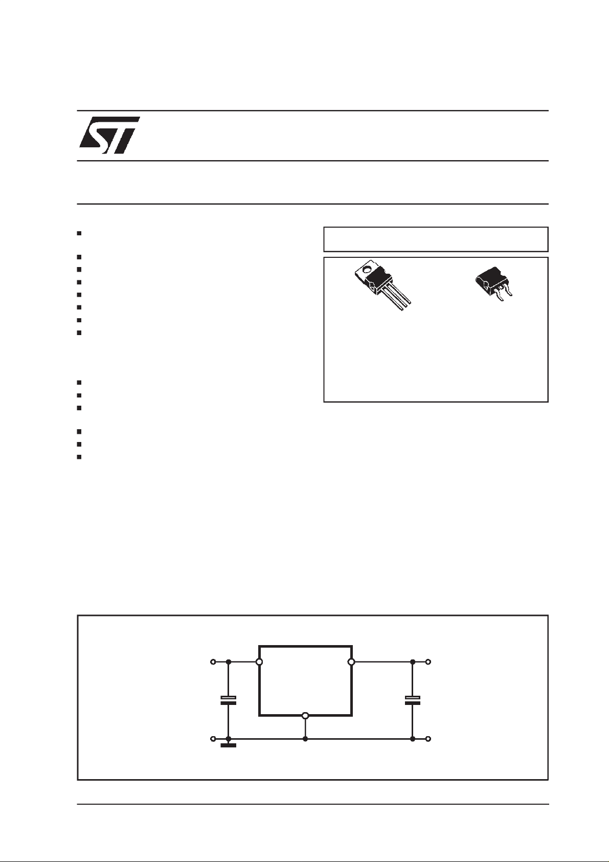
1
D2PAKVersawatt TO-220
ORDERING NUMBERS:
L4957AV1.5 L4957AD1.5
L4957AV1.8 L4957AD1.8
L4957AV2.5 L4957AD2.5
L4957AV3.3 L4957AD3.3
plies required by processor, for example they are
the cost effective and efficient solution for conversion from 3.3V (rail bus) to 2.5V @ 2.5A or to
1.5Vwith highcurrent rating.
Fast response transient minimise the output ca-
pacitor value. A minimum of 22µF assures the
stabilityin all load conditions.
The on-chip trimming technique offers a tighter
voltage reference tolerance (with ±
2% including
line and load variation) beside to ensure a controlled short circuit current. Thermal shutdown
provides protection against overload conditions
that creates excessivejunction temperature.
TYPICAL APPLICATION
3V to 14V
OUTIN
1
3
V
OUT
L4957A
C1
May 2000
This is preliminary information on a new product now in development. Details are subject to change without notice.
2
GND
D00IN1107A
C2
1/7
L4957A
ABSOLUTE MAXIMUM RATINGS
Symbol Parameter Value Unit
V
IN
T
i
T
stg
PINSCONNECTION
SupplyInput Voltage 16 V
JunctionTemperature -40 to +150 °C
Storage Temperature -40 to +150 °C
Versawatt (TO220)
BLOCKDIAGRAM
V
IN
10µF
IN
1
3
2
1
PRE
REGULATOR
D98IN838B
V
REF
+
E/A
-
OUT
GND
IN
CURRENT
LIMIT
CHARGE
PUMP
BUFFER
THERMAL
SHUTDOWN
3
2
1
D2PAK
POWER
DMOS
200mΩ
R
X
GND
3
OUT
IN
D98IN933A
OUT
V
22µF
OUT
R
Y
2
GND
D00IN1108A
PIN FUNCTIONS
Pin N° Name Function
1 IN Unregulated input voltage; this pin must be bypassed with acapacitor larger than 10µF.
2 GND To connect to Ground to get 1.5V, 1.8V, 2.5V or 3.3V output.
3 OUT Regulated output voltage. A minimum bypass capacitor of 22µF is required to insurestability.
2/7
THERMALDATA
Symbol Parameter TO220 D2PAK Unit
R
th j-case
R
th j-amb
Thermal Resistance Junction-case Max. 2.5 3 °C/W
Thermal Resistance Junction-ambient Max. 50 60 °C/W
Thermal Shutdown Typ. 150 °C
Thermal Hysteresis Typ. 20 °C
ELECTRICAL CHARACTERISTICS (Tj=25°C, VIN= 5V, unlessotherwise specified).
•
= Specificationsreferred to TJfrom 0°Cto +125°C.
Symbol Parameter Test Condition Min. Typ. Max. Unit
V
IN
V
O
DSON Drain-Source ON
R
I
O
I
Q
OperatingSupply Voltage 3 14 V
Output Voltage 3.15V < VIN< 5.25V;IO=0.1A 1.485 1.5 1.515 V
=3.3V±5%;0.1A< I
V
IN
=3.3V ±5% IO= 0.1A
V
IN
V
=5V±5%
IN
=3.3V ±5% (0.1A< IO< 45A)
V
IN
V
=5V±5% 0.1A< IO<5A
IN
V
=3.3V ±5% IO= 0.1A
IN
V
=5V±5%
IN
=3.3V ±5% (0.1A< IO<2.2A)
V
IN
V
=5V±5% 0.1A< IO<5A
IN
V
=5V±5% IO= 0.1A 3.267 3.3 3.333 V
IN
=5V±5% 0.1A< I
V
IN
<5A • 1.47 1.5 1.53 V
O
1.782 1.8 1.818 V
•
1.764 1.8 1.836 V
2.475 2.5 2.525 V
•
2.45 2.5 2.55 V
<5A • 3.234 3.3 3.366 V
O
•
300 mΩ
Resistance
Current Limiting • 5.1 6.3 7.5 A
Quiescent Current 3V < V
Ripple Rejection f = 120Hz, I
V
< 14V • 0.6 2 mA
IN
=1A
=5V∆VIN=2V
IN
O
PP
60 75 dB
L4957A
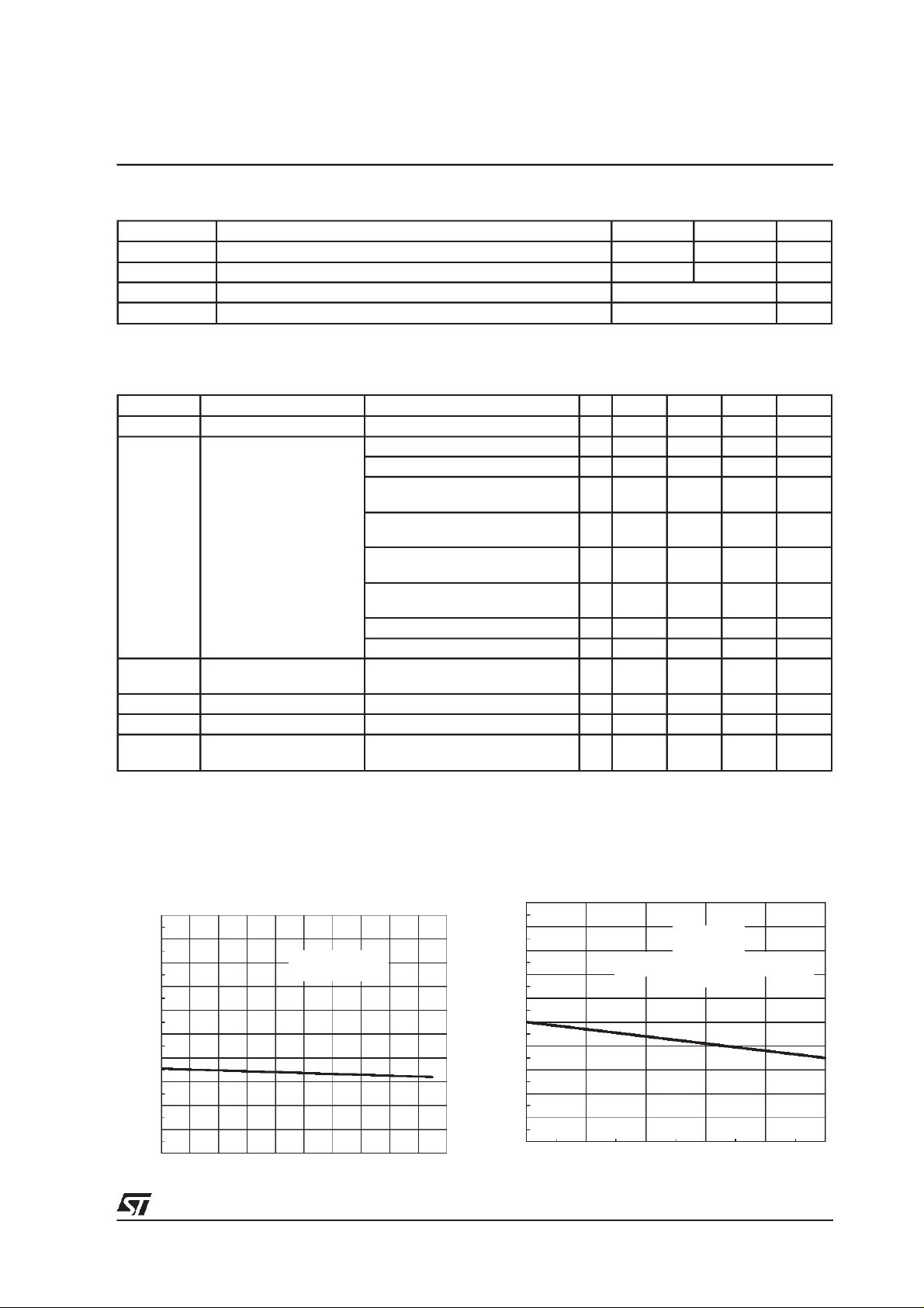
Figure1: Line Regulation vs. Junction
Temperature
5
4.5
4
3.5
3
2.5
2
Output Voltage Deviation [mV]
1.5
1
0.5
0
-40 -20 0 20 40 60 80 100 120 140 160
3V < Vin < 6.5V
Iout = 10mA
Tj[°C]
Figure2: Load Regulation
5
4
3
2
1
0
Output Voltage Deviation [mV]
-1
-2
-3
-4
-5
012345
(Pulsed technique has been used)
Vin = 5V
Tj = 25 °C
Vout= 1.5V
Iout [A]
3/7
 Loading...