

L4956
5A LOW DROP LINEAR REGULATOR
SPLITTED SUPPLY VOLTAGE FOR IMPROVED EFFICIENCY:
-V
PW: 3V MIN. POWER SUPPLYVOLTAGE
SIG: 4.5VMIN.SIGNALSUPPLYVOLTAGE
-V
5A OUTPUTCURRENT
FASTLOAD TRANSIENT RESPONSE
0.75VTYP.DROPOUT VOLTAGE AT5A
INHIBITWITH ZEROCURRENT COMSUMPTION
POWERGOOD
SHORTCIRCUIT PROTECTION
THERMALSHUTDOWN
HEPTAWATTPACKAGE
APPLICATIONS
PENTIUM AND POWERPC SUPPLIES
LOW COST SOLUTION FOR 3.3V TO 1.5V
CONVERSION
SUITABLE FOR APPLICATIONS WITH
STAND BY FEATURE
DESCRIPTION
The L4956 is an adjustablemonolithiclinearregulator designedto satisfy very heavy load transient
and efficient power conversionfrom 3.3V to1.26V
and lower, up to 5A.
MULTIPOWER BCD TECHNOLOGY
HEPTAWATT
ORDERING NUMBER: L4956
Designed in BCDII technology, it uses a charge
pump techniqueto have a properinternal N-channel gate drive. The signal supply voltage input
can operate from 4.5V up to an absoluteof
V
SIG
7V and the power supply voltage input V
PW
can
opearte from 3V min to an absolute of 7V. An
RDSON of 150mV gives a voltagedrop of 750mV
at 5A of loadcurrent.
Very fast load transients and ±1% of reference
voltage precision makes this device suitable for
supplying last micrprocessors generation and low
voltagelogics.
The Heptawatt package enriches the device with
auxiliaryfunctions like power good and inhibit.
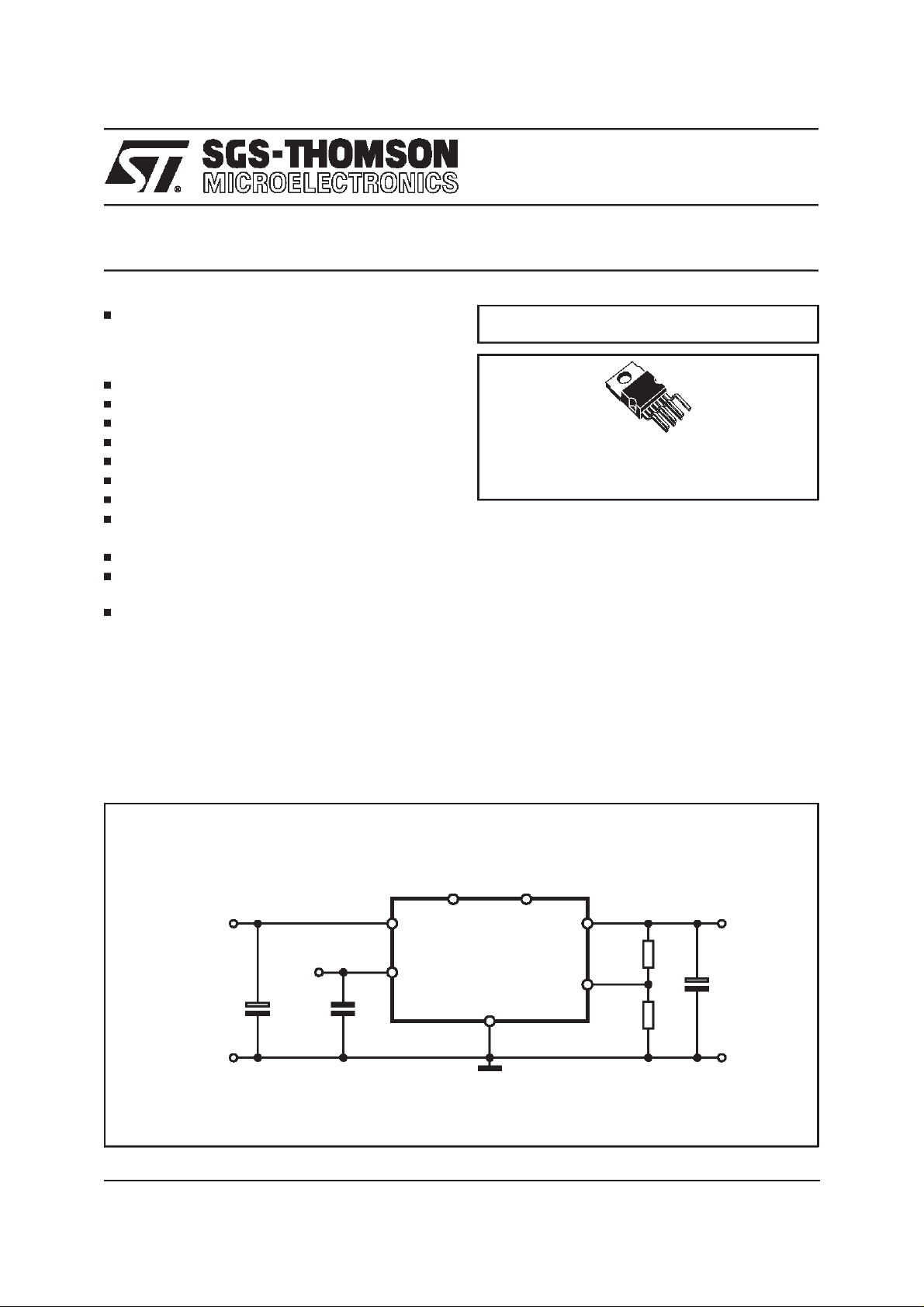
TYPICALAPPLICATION
VPW=3.3Vbus
C
1
March 1998
V
SIG
5Vbus
INH PG
V
PW
=
V
SIG
C
3
36
1
2
L4956
4
GND
OUT
7
ADJ
5
D96IN374B
V
O
R
1
C
2
R
2
1/8
L4956
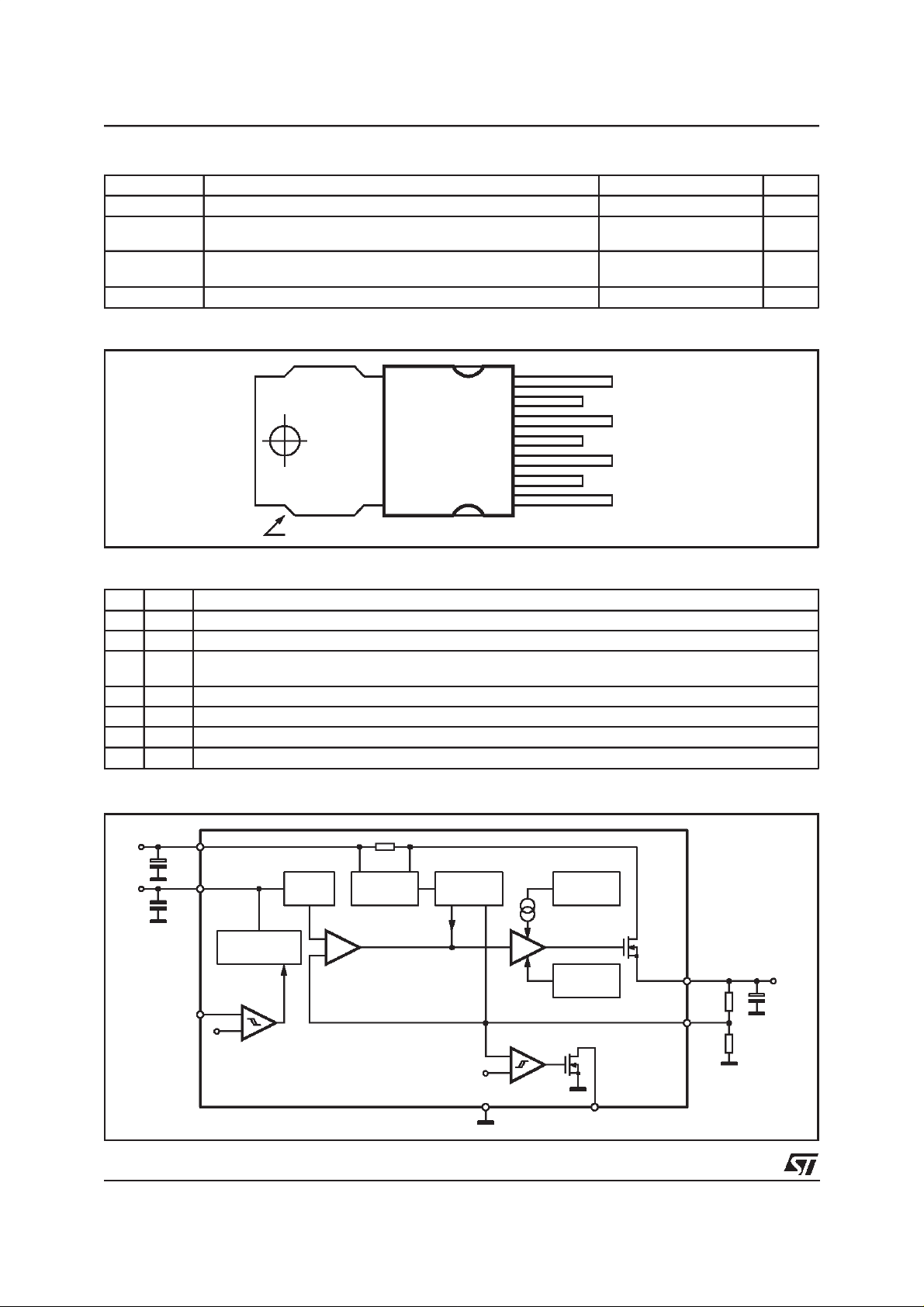
ABSOLUTE MAXIMUM RATINGS
Symbol Parameter Value Unit
V
PW,VSIG
P
TOT
T
st,Ti
PIN CONNECTION(Top view)
Supply Input Voltage 7 V
ADJ pin
PG and INH pins
Power Dissipation @ T
Power Dissipation @ T
amb
case
=50°C
=90°C
-0.3 to 4
0toV
SIG
2
15
Storage Temperature -40 to +150 °C
7 OUT
6
5
4
3
2
1
PG
ADJ
GND
INH
V
SIG
V
PW
V
V
W
W
tab connected to pin 4
D96IN373
PIN FUNCTIONS
No. Name Function
1V
2V
Unregulated power input voltage; this pin must be bypassed witha capacitor larger than10µF.
PW
Unregulated signal input voltage this pin has to be by passed with a minimum capacitor of0.1µF.
SIG
3 INH TTL-CMOS input. A logic level on this input disable the device. An internal pull-down insures insures
full functionally even if the pin is open.
4 GND Ground.
5 ADJ The output is connected directly to this terminal for 1.26V operation via divider for higher voltages.
6 PG Opendrainoutput, this pin is low when theoutputvoltageis lowerthan 90%,otherwise ishigh.
7 OUT Regulated output voltage.A minimum bypass capacitor of 22µF is required to insure stability.
BLOCK DIAGRAM
V
V
SIG
INH
PW
1
2
REGULATOR
3
1.26V
INHIBIT
ACTIVE HIGH
PRE
V
REF
1.26V
=
+
E/A
-
CURRENT
LIMITATION
FOLDBACK
0.9V
REF
+
-
4
GND PG
CHARGE
BUFFER
THERMAL
SHUTDOWN
PUMP
6
POWER
DMOS
150mΩ
D96IN372A
OUT
7
R1 22µF
ADJ
5
R2
V
V
PW
10µF
SIG
V
OUT
2/8
THERMAL DATA
Symbol Parameter Value Unit
R
th j-pins
R
th j-amb
Thermal ResistanceJunction-case 2.5 °C/W
Thermal ResistanceJunction-ambient 50 °C/W
Thermal Shutdown Typ. 150 °C
Thermal Hysteresis Typ. 20 °C
ELECTRICALCHARACTERISTICS (Tj=25°C,unless otherwisespecified)
Symbol Parameter Test Condition Min. Typ. Max. Unit
V
PW
V
SIG
V
OUT
∆V
OUT
∆V
OUT
I
O
I
Q
(1) Output voltage connected to ADJ.
PowerOperatingSupplyVoltage 3 6.5 V
Signal Operating Supply Voltage 4.5 6.5 V
Output Voltage (1) 0 < Tj < 125°C; VPW= 3.3V
4.5V< V
3V< V
0.1A < I
< 6.5V; 0.1A< IO<5A
SIG
<5.5V;4.5V< V
PW
< 5A; 0 < Tj< 125°C
O
SIG
<6.5V
Line regulation (1) 3V < VPW< 5.5V; IO= 10mA
4.5V< V
Load regulation (1) VPW = 3.3V; V
0.1A < I
Drop-out Voltage I
=5A
O
I
= 5A, Tj= 125°C
O
SIG
O
<6.5V
<5A
SIG
=5V
1.240 1.260 1.280 V
1.224 1.260 1.296 V
0.5 3 mV
15mV
0.75
1.1
1.1
1.5
Current Limiting 0 < Tj< 125°C 5.1 6.3 7.5 A
Short Circuit Current V
Quiescent Current at pin V
Stand By Current at pin V
SIG
SIG
= 0V, 0 < Tj< 125°C 1.8 A
O
0.1A < IO<5A
4.5V < V
SIG
<6.5V
INH = HIGH V
= 5V 100 150 µA
SIG
1.5 3 mA
Inhibit Threshold 0 < Tj < 125°C 1.1 1.26 1.42 V
Inhibit Histeresys 0.2 V
Inhibit Bias Sink Current 5 10 µA
Power Good Threshold 0.9x
V
OUT
Power Good Saturation I
= 4mA 0.1 0.4 V
6
Power Good Histeresys 0.2 V
L4956
V
V
V
3/8
 Loading...