

L4955
5A ULDO LINEAR REGULATORS FAMILY
UP TO 5A OUTPUTCURRENT
2% PRECISEOUTPUT VOLTAGES
±
FASTTRANSIENTRESPONSE
0.75VTYP. DROP OUT VOLTAGEAT 5A
OPERATINGINPUT VOLTAGEFROM 4.5V
ADJUSTABLEVERSION:
= 1.26V
• V
O
• INHIBIT(I
POWERGOOD
•
PROGRAMMABLECURRENT LIMIT
•
= 120µA TYP.)
Q
• HEPTAWATT PACKAGE
FIXED VERSION:
• 3.3V,5.1V OUTPUTS
VERSAWATTPACKAGE
•
VERYLOW QUIESCENTCURRENT
SHORT CIRCUIT PROTECTION (Foldback
function)
THERMALSHUTDOWN
APPLICATIONS
PENTIUMANDPOWER PCSUPPLIES
POSTREGULATOR FOR SMPS
LOW COST SOLUTION FOR 5V TO 3.3V
CONVERSION
LOW COST BATTERYCHARGER
CONSTANT CURRENT REGULATOR
SUITABLE FOR APPLICATION WITH
STANDBYFEATURE
DESCRIPTION
The L4955 is a familyof monolithic ultra very low
drop linear regulators designed to supply the
most recent microprocessors.
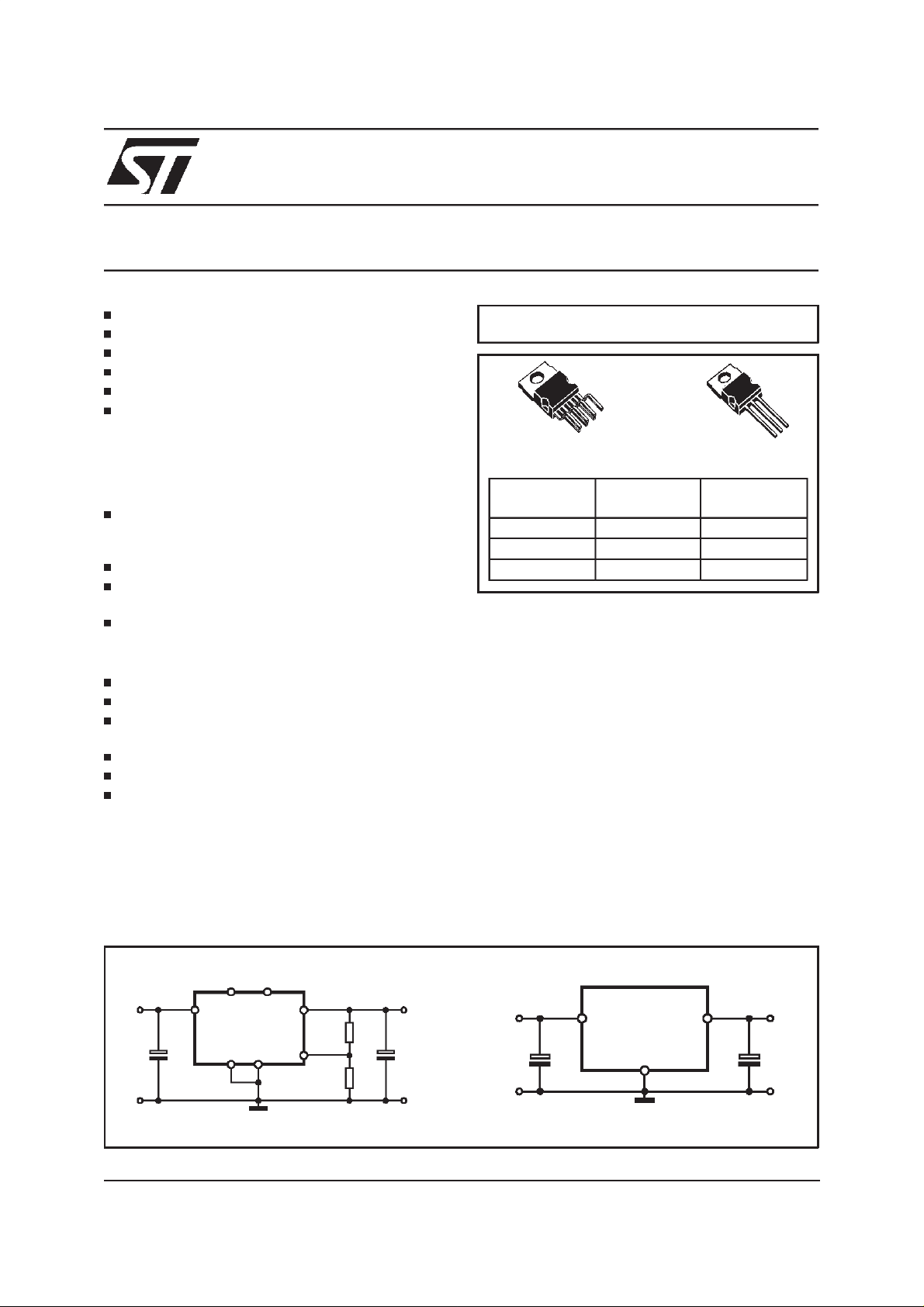
TYPICALAPPLICATIONS
MULTIPOWER BCD TECHNOLOGY
HEPTAWATT VERSAWATT
ORDERING
NUMBERS
L4955 1.26V ADJ HEPTAWATT
L4955V3.3 3.3V VERSAWATT
L4955V5.1 5.1V VERSAWATT
OUTPUT
VOLTAGE
(TO-220)
PACKAGE
The dropout voltage is only 0.75V (Typ.) at 5A, directly dependenton the output current conditions.
Realized in BCDII technology, it has on board a
charge pump to properly drive an N-channel
powermos Transistorwith 150mΩof R
DSON
.
It operates from a 4.5V minimum supply, with a
very low quiescent current irrespective of the
load; a minimum of 22µF output capacitor is required for stability.
The on-chip trimming techniques improve the precisionof the availableoutputvoltages to±2%.
Ancillary functions like power good, inhibit with
low power consumption, programmable output
voltage and current limiting make the flexible
heptawatt version usable in applications where
power management, stand-by, features, post
regulation and adjustable current generators for
batterychargers are important.
V
IN
C1
February 1999
INH PG
1
CL GND
63
L4955
24
OUTIN
7
R1
ADJ
5
R2
D97IN589
C2
V
OUT
V
IN
C1
1
L4955VXXX
2
GND
3
D97IN590
OUTIN
C2
V
OUT
1/14
L4955
ABSOLUTE MAXIMUM RATINGS
Symbol Parameter Value Unit
V
IN
P
TOT
T
st,Ti
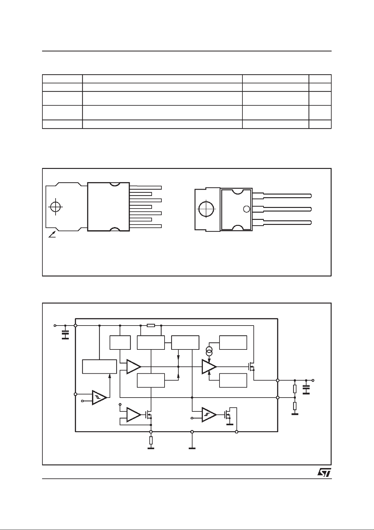
PIN CONNECTIONS (Top views)
tab connected to pin 4
Supply InputVoltage 24 V
ADJ and CL pins
PG and INH pins
Power Dissipation @ T
Power Dissipation @ T
amb
case
=50°C
=90°C
-0.3 to 4
0toV
2
15
IN
Storage Temperature -40 to +150 °C
7 OUT
6
5
4
3
2
1
D96IN367
PG
ADJ
GND
INH
CL
IN
3
1
D96IN369
V
V
W
W
OUT
GND
IN
HEPTAWATT
BLOCK DIAGRAM
10µF
IN
1(1)
REGULATOR
3
INH
1.26V
ACTIVE HIGH
PIN x =
PIN (x) = VERSAWATT
INHIBIT
V
IN
PRE
HEPTAWATT
V
REF
1.26V
V
REF
=
+
-
+
-
(1/4W, 1%)
VERSAWATT
(TO220)
FIXED
C.L.
E/A
PROGRAM.
C.L.
26
RCL
FOLDBACK
0.9V
REF
4(2)
+
-
GND PGCL
CHARGE
BUFFER
THERMAL
SHUTDOWN
PUMP
POWER
DMOS
150mΩ
D96IN366
OUT
7(3)
ADJ
5
R1 22µF
R2
V
OUT
2/14
PIN FUNCTIONS
HW VW Name Function
1 1 IN Unregulated input voltage; this pin must be bypassed with a capacitor larger than 10µF.
2 – CL A resistor connected between this pin and ground sets the programmable current limiting
value. When the programmable current limiting is not used the pin must be connected to GND.
3 – INH TTL-CMOS input. A logic high level on this input disables the device. An internal pull-down
insures full functionally even if the pin is open.
4 2 GND Ground.
5 – ADJ The output is connected directly to this terminal for 1.26V operation; it is connected to the
output through a resistivedivider for higher voltages.
6 – PG Opendrainoutput, this signal islow when the outputvoltage is lower than 90%,otherwise is high.
7 3 OUT Regulated output voltage. A minimum bypass capacitor of 22µF is requiredto insure stability.
L4955
THERMAL DATA
(HEPTAWATT& VERSAWATTpackages)
Symbol Parameter Value Unit
R
th j-case
R
th j-amb
Thermal ResistanceJunction-case Max. 2.5 °C/W
Thermal ResistanceJunction-ambient Max. 50 °C/W
Thermal Shutdown Typ. 150 °C
Thermal Hysteresis Typ. 20 °C
L4955 - ELECTRICAL CHARACTERISTICS (Tj=25°C, Vin= 12V, unless otherwise specified).
•
= Specificationsreferredto TJfrom0°Cto +125°C.
Symbol Parameter Test Condition Min. Typ. Max. Unit
V
IN
V
O
V
∆
∆V
V
O
I
O
I
Q
(1) Output voltage connected to ADJ.
OperatingSupply Voltage 4.5 22 V
Output Voltage (1) 0.1A< IO<5A; 4.5V< VIN<12V 1.235 1.26 1.285 V
4.5V < V
Line regulation (1) 4.5V < VIN<22V; IO= 10mA 2 10 mV
O
Load regulation (1) 0.1A < IO < 5A 2 10 mV
O
<12V; 0.1A< I
IN
Dropout Voltage IO=5A
V
4.5V
≥
IN
=2A • 0.55 0.75 V
I
O
<5A • 1.222 1.26 1.298 V
O
0.75 1.1 V
• 1.1 1.5 V
Current Limiting • 5.1 6.3 7.5 A
Short Circuit Current V
Programmable Current
Limiting
Quiescent Current 0.1A < IO<5A CL=0
=0V • 1.8 A
O
R
R
lim
lim
= 13kΩ
= 47k
Ω
•
•
2.55
0.7030.85
2
C
= 13k
L
2.7
Stand By Current INH = 5V 120 200
Inhibit Threshold Rising Edge
• 1.1 1.26 1.42 V
Inhibit Hysteresis 0.2 V
Inhibit Bias Sink Current INH = 5V or 0.8V 20 60
Power Good Threshold Rising Edge 0.9x V
Power Good Hysteresis
Power Good Saturation I
PG
= 4mA
Ripple Rejection f = 120Hz,I
V
=6V∆VIN=2V
IN
O
=5A
PP
• 0.2 V
•
60 75 dB
O
0.1 0.4 V
3.45
1.00
3
4
A
A
mA
mA
µ
µ
V
A
A
3/14
L4955
L4955V3.3 - ELECTRICAL CHARACTERISTICS
•
= Specificationsreferredto TJfrom0°Cto +125°C.
=25°C, Vin= 5V,unless otherwise specified)
(T
j
Symbol Parameter Test Condition Min. Typ. Max. Unit
V
V
∆
∆V
IN
O
V
I
O
I
Q
Operating Input Voltage 4.5 22 V
Output Voltage 4.75V< VIN<12V; 0.1A< IO< 5A 3.234 3.300 3.366 V
4.75V< V
Line regulation 4.5V < VIN<12V; IO= 10mA 2 10 mV
O
Load regulation 0.1A < IO < 5A 3 15 mV
O
<12V; 0.1A< I
IN
<5A • 3.201 3.300 3.399 V
O
Current Limiting • 5.1 6.3 7.5 A
Short Circuit Current V
=0V • 1.8 A
O
Quiescent Current 0.1A < IO<5A 2 3 mA
Ripple Rejection f = 120Hz,I
V
=6V∆VIN=2V
IN
O
=5A
PP
57 70 dB
L4955V5.1 - ELECTRICAL CHARACTERISTICS (Tj=25°C, Vin= 8V,unless otherwise specified)
•
= Specificationsreferredto TJfrom0°Cto +125°C.
Symbol Parameter Test Condition Min. Typ. Max. Unit
V
IN
V
O
V
D
Operating Input Voltage VO+V
D
Output Voltage 6.75V< VIN<15V; 0.1A< IO< 5A 5.000 5.100 5.200 V
6.75V < V
< 15V; 0.1A< I
IN
<5A • 4.950 5.100 5.250 V
O
Drop-out Voltage IO= 5A 0.75 1.1 V
22 V
• 1.1 1.5 V
=2A • 0.55 0.75 V
I
O
∆V
∆V
I
O
I
Q
Line regulation 6.5V < VIN<15V; IO= 10mA 2 10 mV
O
Load regulation 0.1A < IO < 5A 5 20 mV
O
Current Limiting • 5.1 6.3 7.5 A
Short Circuit Current V
=0V • 1.8 A
O
Quiescent Current 0.1A < IO<5A 2 3 mA
Ripple Rejection f = 120Hz,I
V
=8V∆VIN=2V
IN
O
=5A
PP
55 65 dB
4/14
L4955
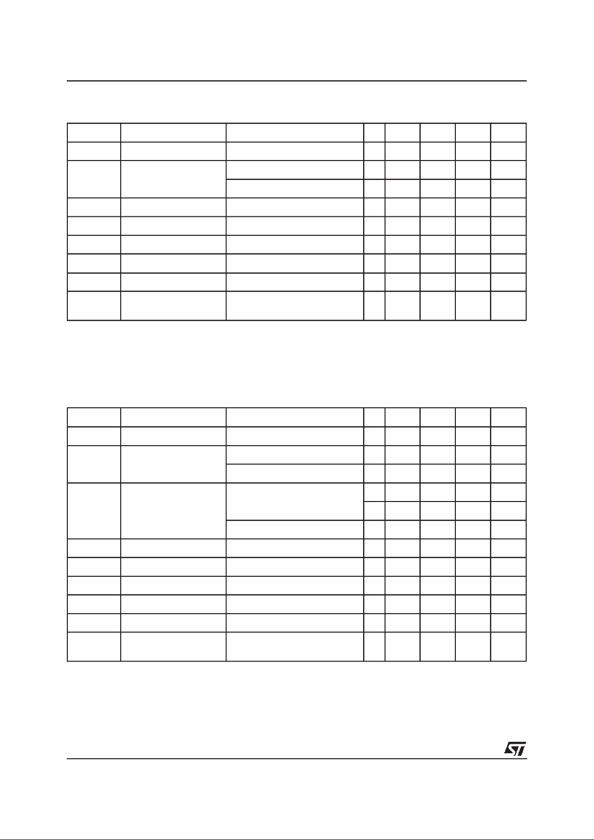
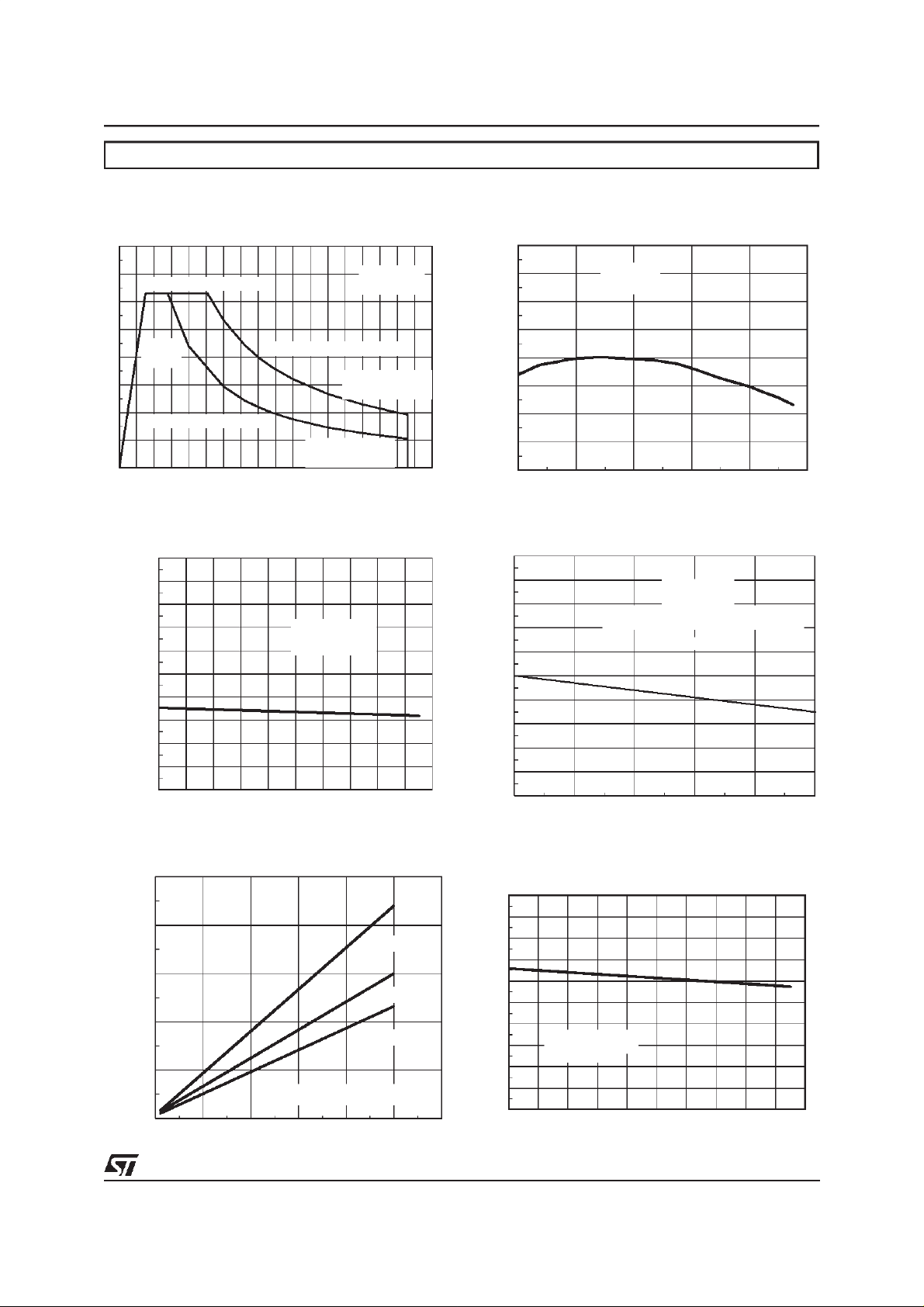
L4955
Figure 1:
Ou tput C urrent [A ]
8
7
6
5
4
3
2
1
0
0 2.5 5 7.5 10 12.5 15 17.5 20 22.5
L4955 DC Operating Area
Current Lim itation
Rdson
limit
DC O perating A rea
Power D issipation Lim it
(Vin - Vout) [V]
Vin > 4.5V
Tj = 125°C
Tc = 25°C
Pdm ax = 40W
Tc = 70°C
Pdmax = 22W
Figure 3: LineRegulationvs. Junction
Temperature
5
4.5
4
3.5
3
2.5
2
1.5
1
Output Voltage Deviation [m V
0.5
0
-40 -20 0 20 40 60 80 100 120 140 160
Figure 5:
1.25
0.75
M in im u m V in - Vo u t Vo lta g e [V ]
0.25
DropoutVoltage
1
0.5
0
0123456
4.5V <Vin<22V
Iout=10mA
Tj[°C]
Tj = 125 °C
Tj= 25 °C
Tj= -40°C
Pulsed techniq ue has b een used
Iout [A]
Figure2:
OutputVoltage Stabilityvs. Junction
Temperature
Vout [V]
1.28
1.275
1.27
1.265
1.26
1.255
1.25
1.245
1.24
-40 0 40 80 120 160
Vin=12V
Iout=10m A
Tj [°C]
Figure4: Load Regulation
5
4
3
2
1
0
-1
-2
Output Voltage Deviation [m V ]
-3
-4
-5
012345
Figure6:
MaximumOutputCurrentvs.Junction
(Pulsed techn ique has been used)
Vin = 12V
Tj= 25 °C
Vo u t = V
Iou t [ A ]
ADJ
Temperatur ewithinternalcurrentlimiti ng
O utp ut C urre n t [A]
10
9
8
7
6
5
4
3
2
1
0
-40 -20 0 20 40 60 80 100 120 140 160
*Pulsed tecnique has been used
(Vin-Vout) > 2V
pin 2 = GND
Tj [°C]
5/14
 Loading...