

MULTIFUNCTIONVERY LOW DROP
OPERATINGDC SUPPLY VOLTAGERANGE
5V - 28V
TRANSIENTSUPPLYVOLTAGEUP TO 40V
EXTREMELY LOW QUIESCENT CURRENT
IN STANDBYMODE
HIGHPRECISIONSTANDBYOUTPUT VOLT-
AGE 5V±1%
OUTPUT CURRENT CAPABILITY UP TO
100mA
VERY LOW DROPOUT VOLTAGE LESS
THAN 0.5V
RESET CIRCUIT SENSING THE OUTPUT
VOLTAGE
PROGRAMMABLE RESET PULSE DELAY
WITH EXTERNALCAPACITOR
VOLTAGESENSECOMPARATOR
THERMAL SHUTDOWN AND SHORT CIR-
CUIT PROTECTIONS
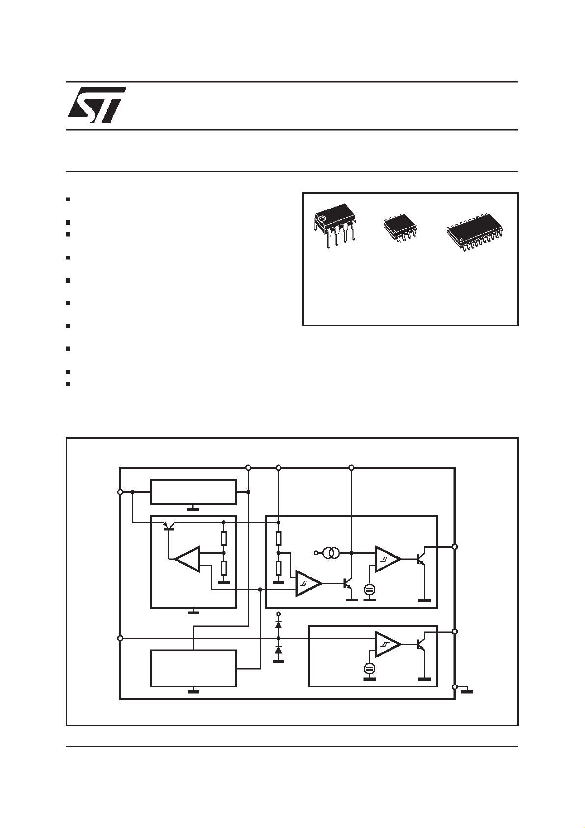
L4949E
VOLTAGEREGULATOR
Minidip SO8
ORDERING NUMBERS:
DESCRIPTION
The L4949E is a monolithic integrated 5V voltage
regulator with a verylow dropoutoutput and additional functions as power-onreset and input voltage sense. It is designed for supplying the microcomputer controlled systems especially in
automotiveapplications.
SO20W (12+4+4)
L4949E (Minidip)
L4949ED (SO8)
L4949EP (SO20W)
BLOCK DIAGRAM
S
SI
PREREGULATOR 5VV
REG
REF
1.23V
V
OUT
Z
+
RESET
V
S
SENSE
CTV
2µ
2V
1.23V
D96AT219
RES
SO
GND
June 2000
1/10
L4949E
ABSOLUTE MAXIMUM RATINGS
Symbol Parameter Value Unit
V
SDC
V
STR
I
V
V
RES,VSO
I
RES,ISO
V
I
T
T
Note: The circuit is ESD protectedaccording to MIL-STD-883C
THERMAL DATA
Symbol Description Minidip SO-8 SO20L Unit
R
th j-amb
R
thj-pins
TJSD Thermal Shutdown Junction temperature 165
DC Operating Supply Voltage 28 V
Transient Supply Voltage(T < 1s) 40 V
Output Current Internally Limited
O
Output Voltage 20 V
O
Output Voltage 20 V
Output Current 5 mA
Preregulator Output Voltage 7 V
Z
Preregulator Output Current 5 mA
Z
Junction Temperature -40 to +150
J
Storage Temperature Range -55 to +150 °C
stg
Thermal Resistance Junction-ambient Max 100 200 50 °C/W
Thermal Resistance Junction-pins Max 15 °C/W
C
°
C
°
PIN CONNECTIONS
V
S
SI
V
Z
CT GND
1
2
3
4
D95AT217
MINIDIP/SO8
V
Z
CT
N.C.
8
7
6
5
V
OUT
SO
RES
GND
GND
GND
GND
N.C.
N.C. V
RES SO
2
3
4
5
6
7
8
9
10
D95AT218
20
19
18
17
16
15
14
13
12
11
SI1
V
S
N.C.
GND
GND
GND
GND
N.C.
OUT
SO20
2/10
L4949E
ELECTRICALCHARACTERISTICS
= 14V; -40°C<Tj< 125°Cunless otherwisespecified)
(V
S
Symbol Parameter Test Condition Min. Typ. Max. Unit
V
V
V
V
DP
V
Output Voltage TJ=25°C; IO= 1mA 4.95 5 5.05 V
O
Output Voltage 6V < VIN<28V, 1mA < IO<50mA 4.90 5 5.10 V
O
Output Voltage VIN=40V;
O
Dropout Voltage IO= 10mA
Input to Output Voltage
IO
T<1s5mA<I
I
= 50mA
O
I
= 100mA
O
V
= 4V, IO= 35mA 0.4 V
IN
<100mA
O
4.75 5.25 V
0.1
0.2
0.3
0.25
0.4
0.5
Difference in Undervoltage
Condition
I
** Max Output Leakage VIN= 25V, VO= 5.5V 20 50 80 µA
outh
V
OL
V
OLO
I
LIM
I
QSE
I
Q
** With thistest we guaranteethat with no output currentthe output voltage will not exceed 5.5V
Line Regulation 6V < VIN< 28V; IO= 1mA 20 mV
Load Regulation 1mA < IO< 100mA 30 mV
Current Limit VO= 4.5V
V
= 4.5V, TJ=25°C
O
V
= 0V (note1)
O
105
120
200
100
400
400
Quiescent Current IO= 0.3mA; TJ< 100°C 200 300
Quiescent Current IO= 100mA 5 mA
RESET
V
V
t
V
I
V
V
CTth, hy
RT
RTH
RD
RL
RH
CTth
Reset Thereshold Voltage VO-0.5 V V
Reset Thereshold Hysteresis 50 100 200 mV
Reset Pulse Delay CT= 100nF; TR≥100µs 55 100 180 ms
Reset Output Low Voltage R
ResetOutput High Leakage Current V
= 10KΩto VOV
RES
=5V 1
RES
1.5V 0.4 V
≥
S
Delay Comparator Thereshold 2 V
Delay Comparator Thereshold
100 mV
Hysteresis
SENSE
V
V
V
mA
mA
mA
µ
µ
A
A
V
V
sth
V
SL
I
SH
I
SI
Sense Low Thereshold 1.16 1.23 1.35 V
st
Sense Thereshold Hysteresis 20 100 200 mV
Sense Output Low Voltage V
Sense Output Leakage VSO= 5V; VSI≥ 1.5V 1 µA
Sense Input Current VSI= 0 -20 -8 -3 µA
PREREGULATOR
V
I
Note 1: Foldback characteristic
Preregulator Output Voltage IZ=10µA 4.5 5 6 V
Z
Preregulator Output Current 10
Z
≤
SI
R
= 10KΩ to V
SO
1.16V;V
3V
≥
S
O
0.4 V
A
µ
3/10
 Loading...