

L4947
5V-0.5A VERY LOW DROP REGULATOR WITH RESET
PRECISE OUTPUT VOLTAGE (5V ± 4%)
OVER FULL TEMPERATURE RANGE
(– 40 / 125
VERY LOW VOLTAGE DROP (0.75Vmax)
OVER FULL T RANGE
OUTPUTCURRENT UP TO 500mA
RESETFUNCTION
POWER-ON RESET DELAY PULSE DE-
FINED BY THE EXTERNALCAPACITOR
+ 80V LOAD DUMP PROTECTION
– 80V LOAD DUMP PROTECTION
REVERSEVOLTAGEPROTECTION
SHORT CIRCUIT PROTECTION AND THER-
MAL SHUT-DOWN (with hysteresis)
LOW STARTUPCURRENT
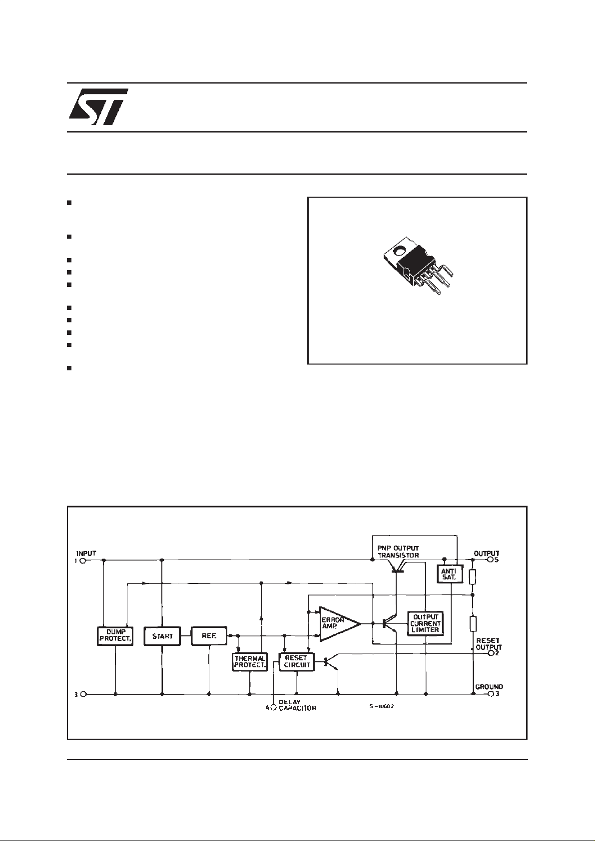
DESCRIPTION
The L4947/L4947R is a monolithic integrated circuit in Pentawatt package specially designed to
provide a stabilizedsupply voltage for automotive
and industrial electronic systems. Thanks to its
very low voltage drop, in automotive applications
the L4947/L4947Rcan work correctly even during
the cranking phase, when the battery voltage
C)
°
L4947R
Pentawatt
ORDERING NUMBERS:
could fall as low as 6V. Furthermore, it incorporates a complete range of protection circuits
against the dangerous overvoltages always present on the battery rail of the car. The reset function makes the device particularlysuited to supply
microprocessorbased systems : a signal is available (after an externally programmable delay) to
reset the microprocessor at power-on phase ; at
power-off, this signal becomes low inhibiting the
microprocessor.
L4947
L4947R
BLOCK DIAGRAM
This is advancedinformation on anew product now in development or undergoingevaluation. Details are subject tochange without notice.
June 2000
1/6
L4947 - L4947R
ABSOLUTE MAXIMUM RATINGS
Symbol Parameter Value Unit
V
i
DC Input Voltage
DC Reverse Input Voltage
Transient Input Overvoltages :
Load Dump :
rise
≥ 0.5Ω
fall
=1µs, t
≤ 10ms
≤ 10ms, R
= 500µs, R
fall
SOURCE
SOURCE
5ms ≤ t
Fall Time Constant = 100ms
τ
f
R
SOURCE
Field Decay :
5ms ≤ t
Rise Time Constant = 33ms
τ
r
Low Energy Spike :
t
rise
Repetition Frequency = 5Hz
f
r
35
–18
80
–80
≥ 10Ω
±100
≥ 10Ω
V
V
V
V
V
V
R
T
J,Tstg
Note: The circuit is ESD protected according to MIL-STD-883C.
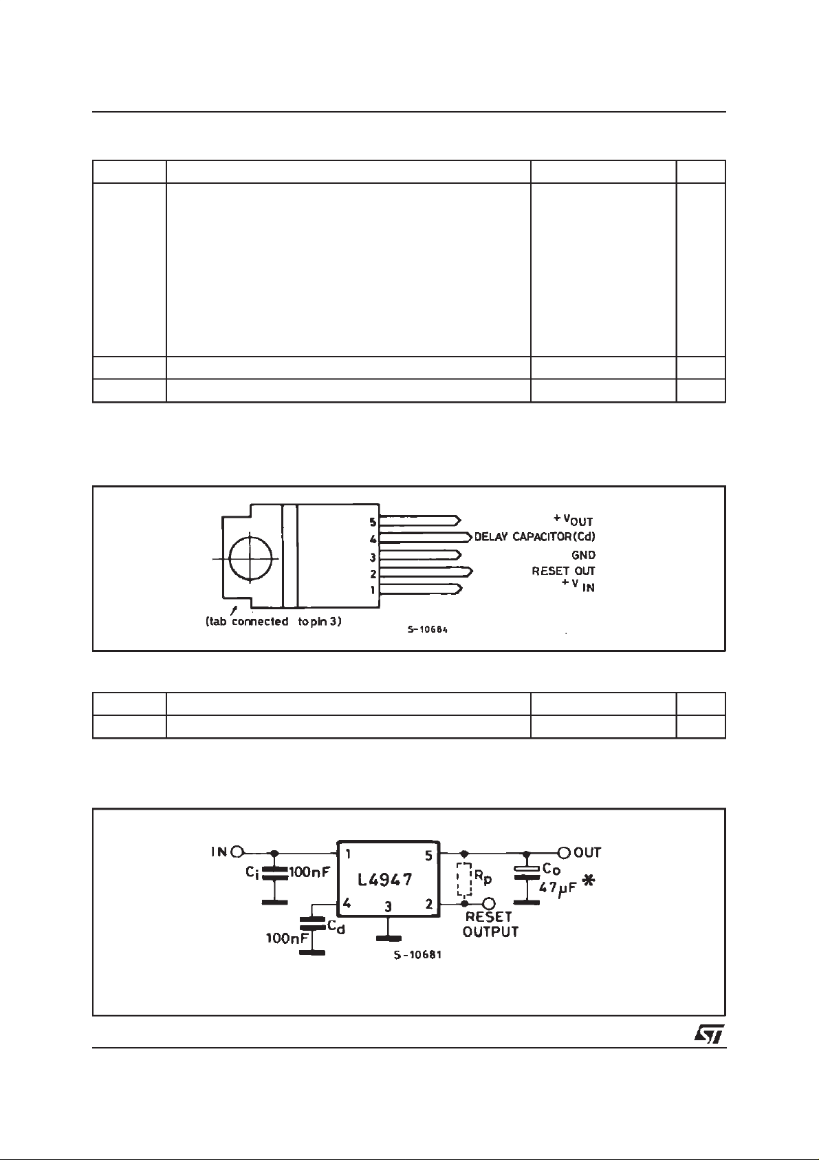
PIN CONNECTION
Reset Output Voltage 35 V
Junction and Storage Temperature Range – 55 to 150 °C
(Top view)
THERMAL DATA
Symbol Parameter Value Unit
R
th j-case
Thermal Resistance Junction-case Max 3.5 °C/W
TEST CIRCUIT
(*) Min.20µF, ESR < 10Ω over full temperaturerange RP(pullup resistor) and RL(load) areboth equal to 1KΩ.
2/6

L4947 - L4947R
ELECTRICALCHARACTERISTICS
R
=1KΩ,RL=1KΩ, –40°C ≤ TJ≤ 125°C, unlessotherwise specified)
p
(refer to the test circuit, V
= 14. 4V, Co=47µF, ESR < 10Ω,
i
Symbol Parameter Test Conditions Min. Typ. Max. Unit
V
o
Output Voltage Io= 0mA to 500mA
4.80
5.00
5.20
Over Full T Range
T
V
i
∆V
∆V
V
i–Vo
I
q
V
∆
T
Operating Input Voltage Io= 0mA to (*) 500mA 6 26 V
Line Regulation Vi= 6V to 26V ;
o
Load Regulation Io= 5mA to 500mA 15 60 mV
o
Dropout Voltage Io= 500mA, TJ=25°C
Quiescent Current Io= 0mA, TJ=25°C
Temperature Output Voltage
o
Drift
SVR Supply Volt. Rej. I
I
V
V
RT peak
sc
R
I
R
Output Short Circuit Current 0.50 0.80 1.50 A
Reset Output Saturation Voltage 1.5V < Vo<V
Reset Output Leakage Current VOinRegulation, VR=5V 50 µA
Power On-Off Reset out Peak
Voltage
V
RT (off)
Power OFF VoThreshold TJ=25°C
=25°C
J
I
= 5mA
o
Over Full T Range
I
= 0mA Over Full T
o
I
= 500mA Over Full T
o
= 350mA ; f = 120Hz
o
C
= 100µF;
o
V
= 12V±5V
i
I
= 1.6mA
R
3.0V < V
I
= 8mA
R
pp
RT (off)
o<VRT (off)
,
,
1KΩReset Pull-up to Vo,TJ=
25°C
L4947: V
@ Reset Out H to L
o
Transition
L4947R: V
@ Reset Out H to
o
4.90
5.00
5.10
210mV
0.40 0.55
0.75
5
6.5
110
10
13
180
– 0.5 mV/°C
50 60 dB
0.40
0.40
0.50 0.80 V
4.70
4.75 Vo–0.15
4.55 Vo–0.30 V
L Transition
V
RT (on)
V
Hyst
V
Power ON VoThreshold Vo@ Reset Out L to H
Transition
Power ON-Off Hysteresis V
d
Delay Comparator Threshold Vd@ Reset Out L to H
RT (on)–VRT (off)
3.65 4.00 4.35 V
V
RT (off)
+ 0.05
V
o
0.04
–
0.05 V
Transition
@ Reset Out H to L
V
d
3.20 3.55 3.90 V
Transition
V
dH
I
d
Delay Comparator Hysteresis 0.45 V
Delay Capacitor Charging
Vd= 3V, TJ=25°C20/µA
Current
V
disch
Delay Capacitor Discharge
Vo<V
RT (off)
0.55 1.20 V
Voltage
T
d
(*)
For aDC voltage 26 < V
Power on Reset Delay Time Cd= 100nF, TJ=25°C 102030ms
< 37Vthe device is not operating
i
V
V
V
V
mA
mA
mA
V
V
V
V
V
FUNCTIONAL DESCRIPTION
The L4947/L4947R is a very low drop 5V/0.5A
voltage regulator provided with a reset function
and therefore particularly suited to meet the requirements of supplying the microprocessor systems used in automotive and industrial applications.
The block diagram shows the basic structure of
the device : the reference,the error amplifier, the
driver, the power PNP, the protection and reset
functions.
The power stage is a Lateral PNP transistor
which allows a very low dropout voltage (typ.
400mV at T
temperature range @ I
=25°C, max. 750mV over the full
J
= 500mA). The typical
O
curve of the dropout voltage as a function of the
junction temperature is shown in Fig. 1 : that is
the worst case, where I
= 500mA.
O
3/6

L4947 - L4947R
The current consumption of the device (quiescent
current) is maximum 13mA - over full T - when no
load current is required.
The internal antisaturation circuit allows a drastic
reduction in the current peak which takes place
during the start up.
The reset function supervisesthe regulator output
voltage inhibiting the microprocessor when the
device is out of regulation and resetting it at the
power-on after a settabledelay. Thereset is LOW
when the output voltage value is lower than the
reset threshold voltage. At the power-on phase
the output voltage increases (see Fig. 2) and when it reaches the power-on V
threshold V
O
RT
(On) - the reset output becomes HIGH after a delay time set by the external capacitor C
. At the
d
power-off the output voltage decreases : at the
V
and V
Figure 1:
threshold value (VO-0.15V typ. for L4947
RT(Off)
-0.3V typ. for L4947R value) the reset out-
O
TypicalDropoutVoltage vs. T
j
(Io= 500mA).
Figure 2:
ResetWaveforms:
(1) WithoutExternalCapacitor C
(2) With ExternalCapacitorC
d
.
d
.
put instantaneously goes down (LOW status) inhibiting the microprocessor.The typical power onoff hysteresisis 50mV.
The three gain stages (operational amplifier,
driver and power PNP) require the external capacitor (C
=20µF) to guarantee the global
omin
stabilityof the system.
Load dump and field decay protections (± 80V),
reverse voltage (– 18V) and short circuit protection, thermal shutdown are the main features that
make the L4947/L4947Rspecially suitable for applicationsin the automotive enviroment.
EXTERNALCOMPENSATION
Sincethe purpose of a voltage regulatoris to sup-
ply and load variations, the open loop gain of the
regulator must be very high at low frequencies.
This may cause instability as a result of the various poles present in the loop. To avoid this instability dominant pole compensation is used to reduce phase shift due to other poles at the unity
gain frequency.The lower the frequency of these
others poles at the unity gain frequency. The
lower the frequency of these other poles, the
greater must be capacitor esed to create the
dominantpole for the same DC gain.
Where the output transistor is a lateral PNP type
there is a pole in the regulation loop at a frequencybtoo low to be compensated by a capacitor which can be integrated. An external compensation is thereforenecessaryso a very high value
capacitor must be connected from the output to
ground.
The paeassitic equivalent series resistance of the
capacitor used adds a zero to the regulationloop.
This zero may compromise the stability of the
system since its effect tends to cancel the effect
of the pole added. In regulatorsthis ESR must be
less than 3Ω and the minimum capacitor value is
47µF.
4/6

L4947 - L4947R
DIM.
MIN. TYP. MAX. MIN. TYP. MAX.
mm inch
A 4.8 0.189
C 1.37
0.054
D 2.4 2.8 0.094 0.110
D1 1.2 1.35 0.047 0.053
E 0.35 0.55 0.014 0.022
E1 0.76 1.19 0.030 0.047
F 0.8 1.05 0.031 0.041
F1 1 1.4 0.039 0.055
G 3.2 3.4 3.6 0.126 0.134 0.142
G1 6.6 6.8 7 0.260 0.268 0.276
H2 10.4 0.409
H3 10.05 10.4 0.396 0.409
L 17.55 17.85 18.15 0.691 0.703 0.715
L1 15.55 15.75 15.95 0.612 0.620 0.628
L2 21.2 21.4 21.6 0.831 0.843 0.850
L3 22.3 22.5 22.7 0.878 0.886 0.894
L4 1.29 0.051
L5 2.6 3 0.102 0.118
L6 15.1 15.8 0.594
0.622
L7 6 6.6 0.236 0.260
L9 0.2 0.008
M 4.23 4.5 4.75 0.167 0.177 0.187
M1 3.75 4 4.25 0.148 0.157 0.167
V4 40°(typ.)
OUTLINE AND
MECHANICAL DATA
Pentawatt V
H3
L
L1
L8
VV
A
B
C
L5
H1
Dia.
L7
L6
D1
V1
R
D
L2
L3
RESIN BETWEEN
V3
R
R
V4
F1
LEADS
H2
E
M1
M
V4
GG1
F
L9
VV
H2
F
E1
E
V4
5/6

L4947 - L4947R
Information furnished is believed to be accurate and reliable. However, STMicroelectronics assumes no responsibility for the consequences
of use of such information nor for any infringement of patents or other rights of third parties which may result from its use. No license is
granted by implication or otherwise under any patent or patent rights of STMicroelectronics. Specification mentioned in this publication are
subject to change without notice. This publication supersedes and replaces all information previously supplied. STMicroelectronics products
are not authorizedfor use as criticalcomponents in lifesupport devices or systems without express written approval of STMicroelectronics.
The ST logo is a registeredtrademark of STMicroelectronics
2000 STMicroelectronics– Printed in Italy– All Rights Reserved
STMicroelectronics GROUP OF COMPANIES
Australia - Brazil- China - Finland - France - Germany- Hong Kong - India- Italy - Japan - Malaysia - Malta- Morocco -
Singapore -Spain - Sweden- Switzerland - UnitedKingdom - U.S.A.
http://www.st.com
6/6
 Loading...