L4947
5V-0.5A VERY LOW DROP REGULATOR WITH RESET
PRECISE OUTPUT VOLTAGE (5V ± 4%)
OVER FULL TEMPERATURE RANGE
(– 40 / 125
VERY LOW VOLTAGE DROP (0.75Vmax)
OVER FULL T RANGE
OUTPUTCURRENT UP TO 500mA
RESETFUNCTION
POWER-ON RESET DELAY PULSE DE-
FINED BY THE EXTERNALCAPACITOR
+ 80V LOAD DUMP PROTECTION
– 80V LOAD DUMP PROTECTION
REVERSEVOLTAGEPROTECTION
SHORT CIRCUIT PROTECTION AND THER-
MAL SHUT-DOWN (with hysteresis)
LOW STARTUPCURRENT
DESCRIPTION
The L4947/L4947R is a monolithic integrated circuit in Pentawatt package specially designed to
provide a stabilizedsupply voltage for automotive
and industrial electronic systems. Thanks to its
very low voltage drop, in automotive applications
the L4947/L4947Rcan work correctly even during
the cranking phase, when the battery voltage
C)
°
L4947R
Pentawatt
ORDERING NUMBERS:
could fall as low as 6V. Furthermore, it incorporates a complete range of protection circuits
against the dangerous overvoltages always present on the battery rail of the car. The reset function makes the device particularlysuited to supply
microprocessorbased systems : a signal is available (after an externally programmable delay) to
reset the microprocessor at power-on phase ; at
power-off, this signal becomes low inhibiting the
microprocessor.
L4947
L4947R
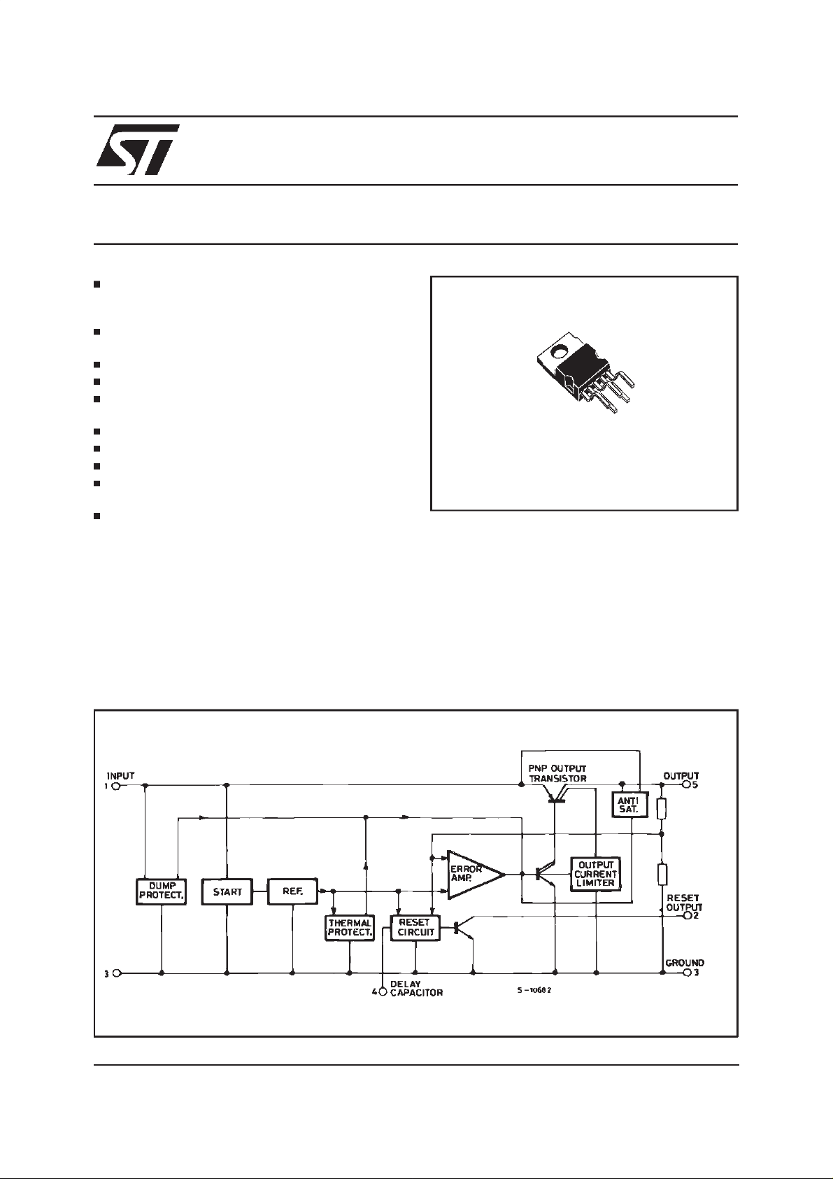
BLOCK DIAGRAM
This is advancedinformation on anew product now in development or undergoingevaluation. Details are subject tochange without notice.
June 2000
1/6

L4947 - L4947R
ABSOLUTE MAXIMUM RATINGS
Symbol Parameter Value Unit
V
i
DC Input Voltage
DC Reverse Input Voltage
Transient Input Overvoltages :
Load Dump :
rise
≥ 0.5Ω
fall
=1µs, t
≤ 10ms
≤ 10ms, R
= 500µs, R
fall
SOURCE
SOURCE
5ms ≤ t
Fall Time Constant = 100ms
τ
f
R
SOURCE
Field Decay :
5ms ≤ t
Rise Time Constant = 33ms
τ
r
Low Energy Spike :
t
rise
Repetition Frequency = 5Hz
f
r
35
–18
80
–80
≥ 10Ω
±100
≥ 10Ω
V
V
V
V
V
V
R
T
J,Tstg
Note: The circuit is ESD protected according to MIL-STD-883C.
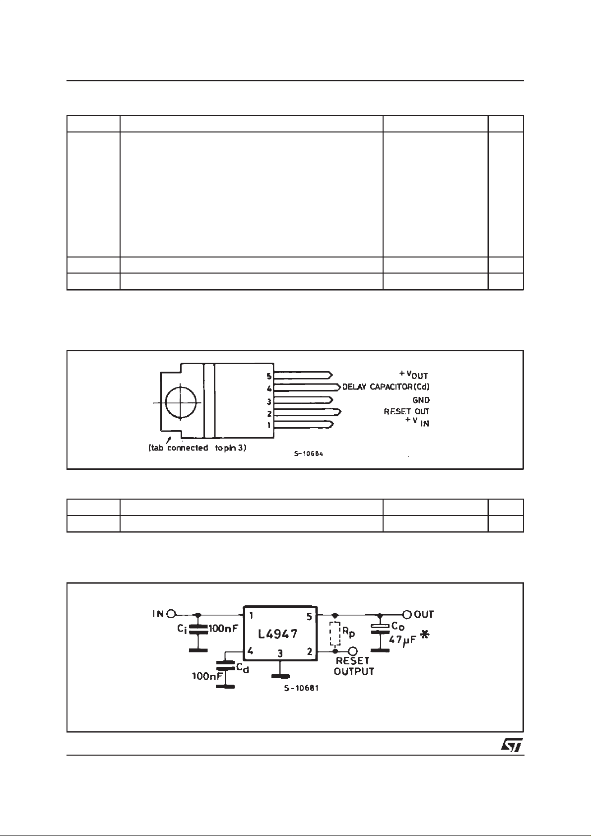
PIN CONNECTION
Reset Output Voltage 35 V
Junction and Storage Temperature Range – 55 to 150 °C
(Top view)
THERMAL DATA
Symbol Parameter Value Unit
R
th j-case
Thermal Resistance Junction-case Max 3.5 °C/W
TEST CIRCUIT
(*) Min.20µF, ESR < 10Ω over full temperaturerange RP(pullup resistor) and RL(load) areboth equal to 1KΩ.
2/6
 Loading...