

SGS Thomson Microelectronics L4940V12, L4940V10, L4940D2T85, L4940D2T5, L4940D2T12 Datasheet
...
VERY LOW DROP 1.5 A REGULATORS
■ PRECISE5V, 8.5V, 10 V,12 V OUTPUTS
■ LOWDROPOUTVOLTAGE(500mV typ
at1.5A)
■ VERYLOW QUIESCENTCURRENT
■ THERMAL SHUTDOWN
■ SHORTCIRCUITPROTECTION
■ REVERSEPOLARITYPROTECTION
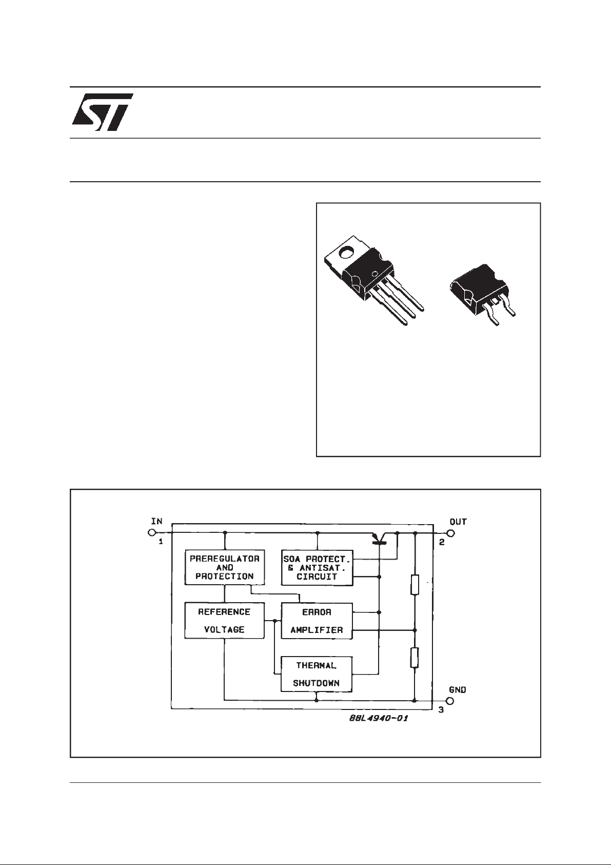
DESCRIPTION
The L4940 series of three terminal positive
regulators is available in TO-220 and D
package and with several fixed output voltages,
making it useful in a wide range of industrial and
consumer applications. Thanks to its very low
input/output voltage drop, these devices are
particularly suitable for battery powered
equipments, reducing consumption and
prolonging battery life. Each type employs
internal current limiting, antisaturation circuit,
thermalshut-down and safe area protection.
2
PAK
TO-220
L4940 series
2
PAK
D
TO-263
BLOCKDIAGRAM
November 1999
1/13
L4940 series
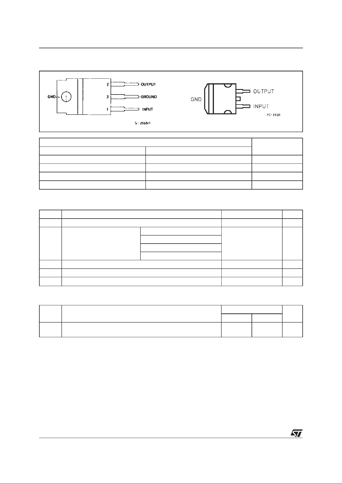
PIN CONNECTION AND ORDER CODES
ORDERING NUMBERS OUTPUT VOLTAGE
TO-220 D
L4940V5 L4940D2T 5 5V
L4940V85 L4940D2 T 85 8.5V
L4940V10 L4940D2 T 10 10V
L4940V12 L4940D2 T 12 12V
ABSOLUTE MAXIMUM RATING
2
PAK
Symbol Description Values Unit
V
ForwardInput Voltage 30 V
I
V
P
T
j,Tstg
Reverse Input Voltage
IR
OutputCurrent Internally Limited
I
O
PowerDissipation Internally Limited
tot
=5V RO=100
V
O
V
=8.5V RO= 180
O
=10V RO= 200
V
O
=12V RO= 240
V
O
Ω
Ω
Ω
Ω
Junctionand StorageTemperature -40 to 150
-15 V
THERMALDATA
Symbol Description Value Unit
2
PAK
3
62.5
o
o
R
thj-cas e
R
thj-amb
Thermal ResistanceJunction-case Max
Thermal ResistanceJunction-ambient Max
TO-220 D
3
50
o
C
C/W
C/W
2/13
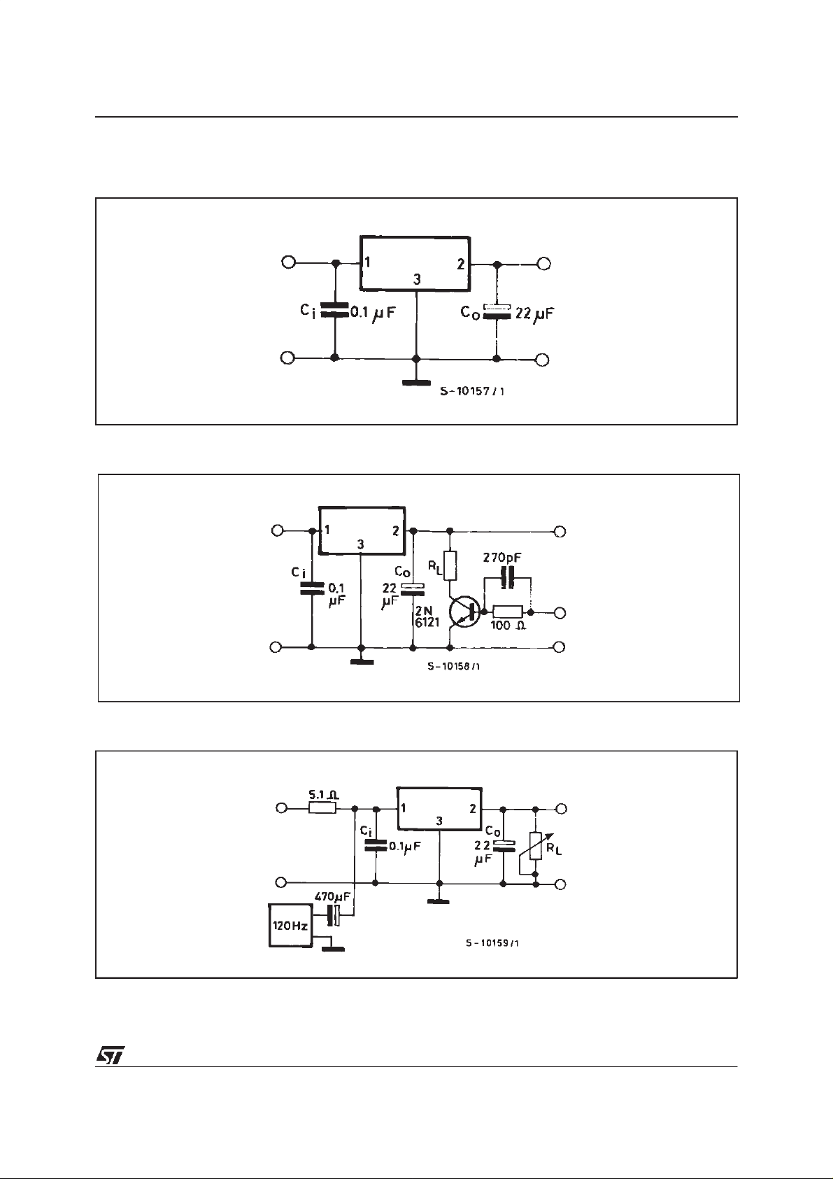
TESTCIRCUITS
Figure1 : DC Parameter.
L4940 series
Figure2 :
Load Rejection.
Figure3 : Ripple Rejection.
3/13
L4940 series
ELECTRICAL CHARACTERISTICS FOR L4940V5
= 7V, Ci=0.1 µF, Co=22µF unless otherwisespecified)
V
i
(refer to the test circuits, T
=25oC,
j
Symbol Parameter Test Conditions Min. Typ. Max. Unit
V
OutputVoltage Io=500 mA 4.9 5 5.1 V
o
V
OutputVoltage Io=5 mA to 1500 mA
o
OperatingInput Voltage Io=5 mA 17 V
V
i
LineRegulation Io=5 mA Vi= 6 to 17V 4 10 mV
V
∆
o
LoadRegulation Io=5 to 1500 mA
V
∆
o
I
Quiescent Current Io=5mA
Q
Quiescent CurrentChange Io=5mA
I
∆
Q
OutputVoltageDrift 0.5 mV/oC
V
∆
o
∆
T
SVR Supply Voltage Rejection I
V
Dropout Voltage Io=0.5A
d
I
ShortCircuitCurrent Vi=14V
sc
= 6.5to 16 V
V
i
=500 to 1000 mA
I
o
=1.5A Vi= 6.5V
I
o
=1.5A Vi= 6.5to 16 V
I
o
=1 A f = 120 Hz 58 68 dB
o
=1.5A
I
o
= 6.5V
V
i
4.855.2V
8
5
5
30
25
15
8
50
3
15
200
500
2
2.2
400
900
2.7
2.9
mV
mA
mA
mV
A
ELECTRICAL CHARACTERISTICS FOR L4940V85(referto the test circuits,Tj=25oC,
= 10.5V,Ci= 0.1 µF, Co=22µF unlessotherwisespecified)
V
i
Symbol Parameter Test Conditions Min. Typ. Max. Unit
V
OutputVoltage Io=500 mA 8.3 8.5 8.7 V
o
V
OutputVoltage Io=5 mA to 1500 mA
o
OperatingInput Voltage Io=5 mA 17 V
V
i
LineRegulation Io=5 mA Vi= 9.5to 17 V 4 9 mV
V
∆
o
∆V
LoadRegulation Io=5 to 1500 mA
o
I
Quiescent Current Io=5mA
Q
Quiescent CurrentChange Io=5mA
I
∆
Q
OutputVoltageDrift 0.8 mV/oC
V
∆
o
T
∆
SVR Supply Voltage Rejection I
V
Dropout Voltage Io=0.5A
d
I
ShortCircuitCurrent Vi=14V
sc
= 10.2to 16V
V
i
I
=500 to 1000 mA
o
=1.5A Vi= 10.2V
I
o
=1.5A Vi= 10.2to16 V
I
o
=1 A f = 120 Hz 58 66 dB
o
=1.5A
I
o
= 10.2V
V
i
8.15 8.5 8.85 V
12
8
4
30
30
16
8
50
2.5
15
200
500
2
2.2
400
900
2.7
2.9
mV
mA
mA
mV
A
4/13

L4940 series
ELECTRICAL CHARACTERISTICS FOR L4940V10
= 12V, Ci= 0.1 µF, Co=22µF unless otherwisespecified)
V
i
(refer to the test circuits,T
=25oC,
j
Symbol Parameter Test Conditions Min. Typ. Max. Unit
V
OutputVoltage Io=500 mA 9.8 10 10.2 V
o
V
OutputVoltage Io=5 mA to 1500 mA
o
OperatingInput Voltage Io=5 mA 17 V
V
i
LineRegulation Io=5 mA Vi=11to17V 3 8 mV
V
∆
o
LoadRegulation Io=5 to 1500 mA
V
∆
o
I
Quiescent Current Io=5mA
Q
Quiescent CurrentChange Io=5mA
I
∆
Q
OutputVoltageDrift 1 mV/oC
V
∆
o
∆
T
SVR Supply Voltage Rejection I
V
Dropout Voltage Io=0.5A
d
I
ShortCircuitCurrent Vi=14V
sc
= 11.7to 16V
V
i
=500 to 1000 mA
I
o
=1.5A Vi= 11.7V
I
o
=1.5A Vi= 11.7to16 V
I
o
=1 A f = 120 Hz 56 62 dB
o
=1.5A
I
o
= 11.7V
V
i
9.6 10 10.4 V
15
10
4
30
35
20
8
50
2
13
200
500
2
2.2
400
900
2.7
2.9
mV
mA
mA
mV
A
A
ELECTRICAL CHARACTERISTICS FOR L4940V12(referto the test circuits,Tj=25oC,
= 14V, Ci= 0.1 µF, Co=22µF unless otherwisespecified)
V
i
Symbol Parameter Test Conditions Min. Typ. Max. Unit
V
OutputVoltage Io=500 mA 11.75 12 12.25 V
o
V
OutputVoltage Io=5 mA to 1500 mA
o
OperatingInput Voltage Io=5 mA 17 V
V
i
LineRegulation Io=5 mA Vi=13to17V 3 7 mV
V
∆
o
∆V
LoadRegulation Io=5 to 1500 mA
o
I
Quiescent Current Io=5mA
Q
Quiescent CurrentChange Io=5mA
∆I
Q
OutputVoltageDrift 1.2 mV/oC
V
∆
o
T
∆
SVR Supply Voltage Rejection I
V
Dropout Voltage Io=0.5A
d
I
ShortCircuitCurrent Vi=14V 2 2.7 A
sc
Z
OutputImpedance f = 1KHz Io=0.5A 40
o
= 13.8to 17V
V
i
=500 to 1000 mA
I
o
=1.5A Vi= 13.8V
I
o
=1.5A Vi= 13.8to16 V
I
o
=1 A f = 120 Hz 55 61 dB
o
=1.5A
I
o
11.5 12 12.5 V
15
10
4
30
35
25
8
50
1.5
10
200
500
400
900
m
mV
mA
mA
mV
Ω
5/13

L4940 series
Figure4 :
Dropoutvoltage vs. Output Current.
Figure6 : Output voltage vs. Temperature
(L4940V5).
Figure5 :
DropoutVoltage vs. Temperature.
Figure7 : Output Voltage vs. Temperature
(L4940V85).
Figure8 :
6/13
Outputvoltagevs. Temperature
(L4040V10).
Figure9 :
OutputVoltage vs. Temperature
(L4940V12).

L4940 series
Figure10 :
QuiescentCurrent vs. Temperature
(L4940V5).
Figure12 : QuiescentCurrent vs. Output Current
(L4940V5).
Figure11 :
QuiescentCurrent vs. Input Voltage
(L4940V5).
Figure13 : Short-circuitCurrent vs. Temperature
(L4940V5).
Figure14 : Peak Output Current vs.
Input/OutputDifferential Voltage (L4940V5).
Figure15 : Low VoltageBehavior (L4940V5 ).
7/13

L4940 series
Figure16 :
LowVoltage Behavior (L4940V85).
Figure17 :
Low Voltage Behavior (L4940V10).
Figure18 : Low Voltage Behavior (L4940V12). Figure 19 : SupplyVoltage Rejection vs.
Frequency (L4940V5).
Figure20 :
8/13
SupplyVoltage Rejection vs.
outputCurrent.
Figure21 :
LoadDump Characteristics
(L4940V5 ).

L4940 series
Figure22 :
Line TransientResponse (L4940V5).
Figure24 : Total Power Dissipation.
Figure23 :
LoadTransient Response.
Figure25 :
DistributedSupply with On-cardL4940 and L4941Low-drop Regulators.
9/13

L4940 series
Figure26 :
ADVANTAGES OF THESE APPLICATIONS ARE :
On card regulation with short-circuit and thermal protection on each output.
Very hightotal system efficiency due to the switching preregulation and very low-drop postregulations.
DistributedSupply with On-cardL4940 and L4941Low-drop Regulators.
Figure27.
ADVANTAGES OF THIS CONFIGURATION ARE :
Very highregulation (line and load) on both the output voltages.
12 V output short-circuit and thermally protected.
Very highefficiency on the 12 V outputdue to the very low drop regulator.
10/13

TO-220 MECHANICAL DATA
L4940 series
DIM.
MIN. TYP. MAX. MIN. TYP. MAX.
A 4.8 0.189
C 1.37 0.054
D 2.4 2.8 0.094 0.110
D1 1.2 1.35 0.047 0.053
E 0.35 0.55 0.014 0.022
F 0.61 0.94 0.024 0.037
F2 1.15 1.4 0.045 0.055
G 4.95 5.08 5.21 0.195 0.200 0.205
H2 10.4 0.409
H3 10.05 10.4 0.396 0.409
L2 16.2 0.638
L3 26.3 26.7 27.1 1.035 1.051 1.067
L5 2.6 3 0.102 0.118
L6 15.1 15.8 0.594 0.622
L7 6 6.6 0.236 0.260
Dia. 3.65 3.85 0.144 0.152
mm inch
P011D
11/13

L4940 series
TO-263 (D2PAK) MECHANICALDATA
DIM.
MIN. TYP. MAX. MIN. TYP. MAX.
A 4.4 4.6 0.173 0.181
A1 2.49 2.69 0.098 0.106
B 0.7 0.93 0.027 0.036
B2 1.14 1.7 0.044 0.067
C 0.45 0.6 0.017 0.023
C2 1.23 1.36 0.048 0.053
D 8.95 9.35 0.352 0.368
E 10 10.4 0.393 0.409
G 4.88 5.28 0.192 0.208
L 15 15.85 0.590 0.624
L2 1.27 1.4 0.050 0.055
L3 1.4 1.75 0.055 0.068
mm inch
12/13
D
A
C2
DETAIL”A”
C
A2
DETAIL”A”
A1
B2
E
L2
L
L3
B
G
P011P6/F

L4940 series
Information furnished is believed tobe accurate and reliable. However, STMicroelectronics assumes no responsibility for the consequences
of use of such information nor for any infringement of patents or other rights of third parties which may result from its use. No license is
granted by implication or otherwise under any patent or patent rights of STMicroelectronics. Specification mentioned in this publication are
subject to change without notice. Thispublication supersedes and replaces all information previously supplied. STMicroelectronics products
are not authorized for use as critical components in life support devices or systems withoutexpress written approval of STMicroelectronics.
The ST logo is a registeredtrademark of STMicroelectronics
1999 STMicroelectronics – Printed in Italy – All Rights Reserved
STMicroelectronics GROUP OF COMPANIES
Australia - Brazil - China - Finland - France - Germany - Hong Kong - India - Italy - Japan- Malaysia - Malta - Morocco
Singapore - Spain- Sweden - Switzerland - United Kingdom - U.S.A.
http://www.st.com
.
13/13
 Loading...