

L4938N/ND
DUAL MULTIFUNCTIONVOLTAGE REGULATOR
.STANDBYOUTPUTVOLTAGEPRECISION5V
± 2%
.
OUTPUT2TRACKEDTOTHESTANDBYOUTPUT
.
OUTPUT 2 DISABLE FUNCTION FOR
STANDBYMODE
.VERY LOW QUIESCENT CURRENT, LESS
THAN 250µA,IN STANDBYMODE
.OUTPUT 2 VOLTAGESETTABLEFROM5 TO
20V
.OUTPUTCURRENTS: I
.
VERYLOWDROPOUT(max 0.4V/0.6V)
=50mA,I02=500mA
01
.OPERATINGTRANSIENT SUPPLYVOLTAGE
UP TO 40V
.POWER-ON RESET CIRCUIT SENSING THE
STANDBYOUTPUT VOLTAGE
.
POWER-ONRESET DELAY PULSEDEFINED
BY THE EXTERNALCAPACITOR
.
EARLYWARNINGOUTPUTFORSUPPLYUNDERVOLTAGE
.
THERMALSHUTDOWNAND SHORTCIRCUIT
PROTECTIONS
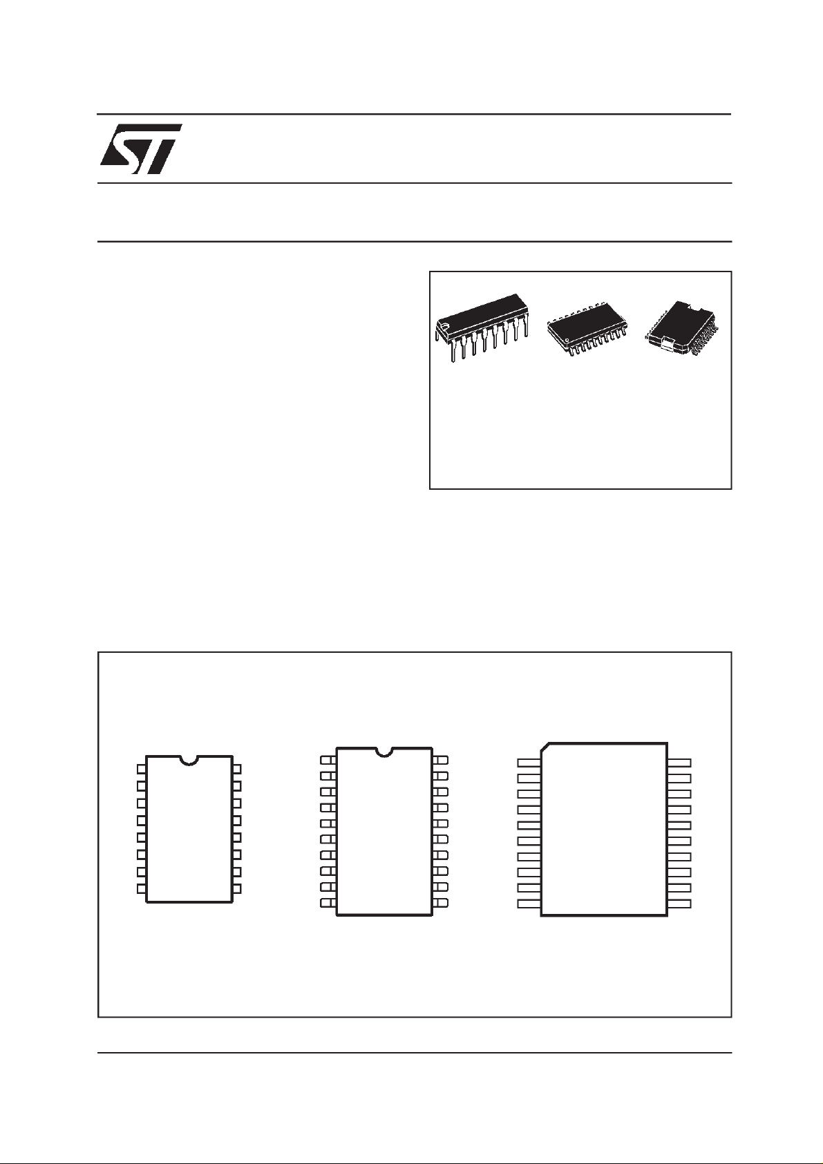
PI N CONNECTION
(top view)
L4 938N PD
PowerDIP
(12+2+2)
ORDERINGNUMBERS: L4938N (PDIP)
DES CRIPTI ON
The L4938Nis a monolithicintegrateddualvoltage
regulatorswithtwoverylowdropoutoutputsandadditionalfunctionssuchas power-onresetand input
voltagesense.Theyare designedfor supplyingmicrocomputer controlled systems specially in automotiveapplications.
SO20
(12+4+4)
L4938ND(SO)
L4938NPD (PSO20)
PowerSO20
POWERDIP
N.C.
GND
GND
RES
V
April 1999
This is advanced information on a new product now in development or undergoing evaluation. Details are subject to change without notice.
1
CT
2
EN
3
4
5
6
SO
7V
8 ADJ9
O1
D95AT156
SI16
V
15
V
14
GND
13
GND
12
V
11
10
N.C.
S1
S2
O2
O2
C7
EN
GND
GND
GND
GND
RES
SO
V
O1
SO20
1
2
3
4
5
6
7
8
9
10
D93AT004
20
19
18
17
16
15
14
13
12
11
SI
V
S1
VS2
GND
GND
GND
GND
VO2
V
O2
ADJ
GND
N.C.
V
S2
V
S1
SI
N.C.
CT
EN
N.C.
GND 10
PowerSO20
1
2
3
4
5
6
7
8
9
D95AT169A
20
19
18
17
16
15
14
13
12
11
GND
N.C.
V
O2
ADJ
V
O1
SO
RESET
N.C.
N.C.
GND
1/12
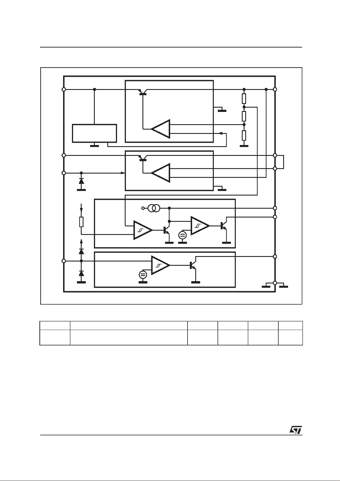
L4938N - L4938ND - L4938NPD
BLOCK DIAG RAM
V
V
EN
S1
REFERENCE
S2
REG1
1.23V
V
O1
V
O2
ADJ
REG2
1.23V
RESET
2µ
2.0V
CT
RES
SI
SENSE
1.23V
(optional)
D94AT143A
THERMAL DATA
Symbol Parameter Powerdip PowerSO20 SO20 Unit
R
thj-case
R
thj-amb
ThermalResistance Junction-Case Max.
ThermalResistance Junction-Ambient Max.
14
90
<2
–
–
20
SO
GND
°
°C/W
C/W
2/12
L4938N - L4938ND - L4938NPD
ABSOLUTE MAXIMUM RATINGS
Symbol Parameter Value Unit
V
T
j,Tstg
I
SI
I
EN
V
EN
V
RES,VSO
I
RES,ISO
P
The circuit is ESD protected according to MIL–STD–883C.
Note :
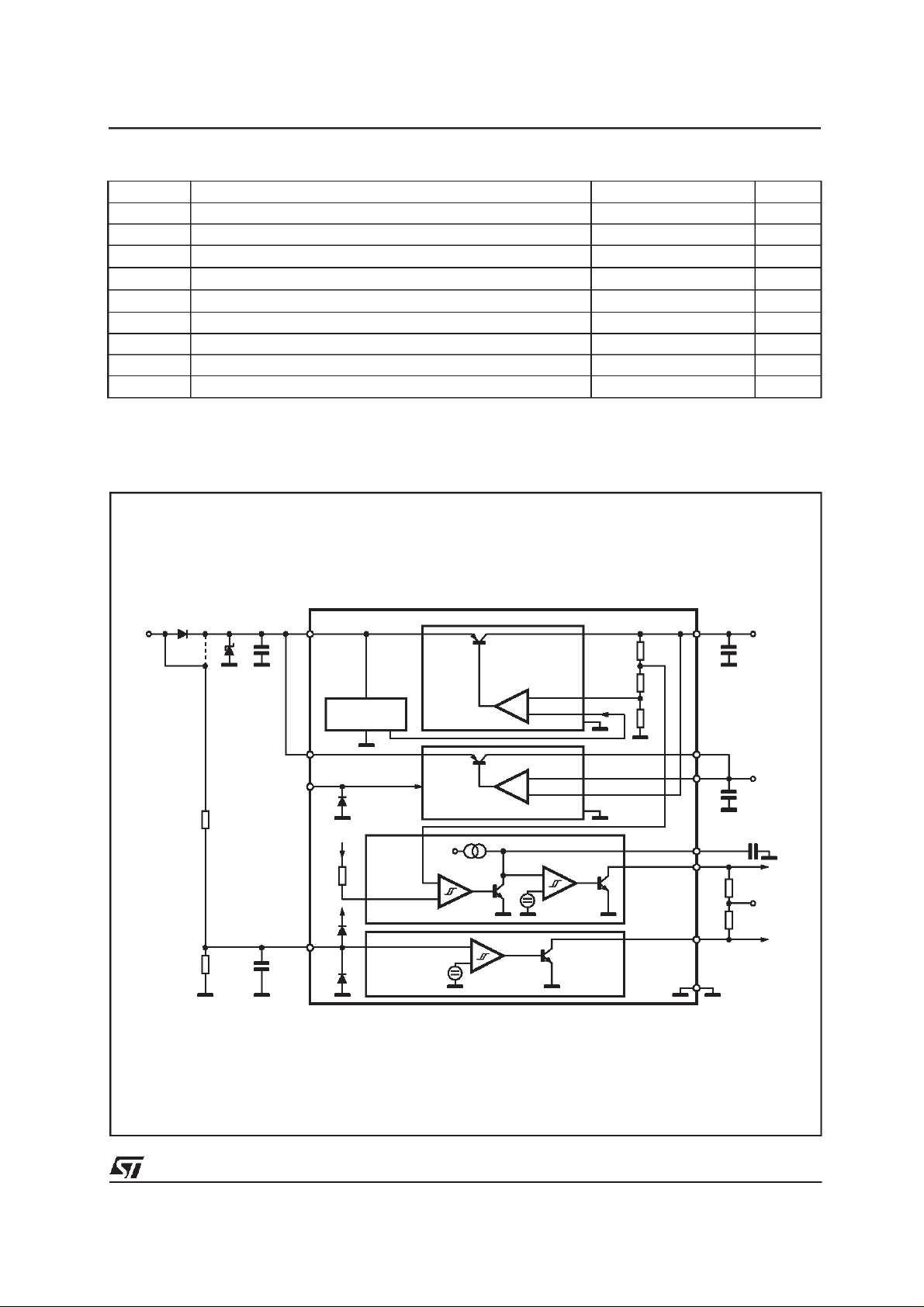
APPLI CATI ON CIRCUI T
DC Supply Voltage 28 V
S
TransientSupply Voltage (T < 1s) 40 V
Junctionand Storage Temperature Range –55 to 150
Sense Input Current (V
≤
SI
0.3V or V
SI>VS
)
1
±
Enable Input Current (VEN≤0.3V) ±1
Enable Input Voltage V
S
Reset and Sense Output Voltage 20 V
Reset and Sense Output Current 5 mA
Power Dissipation 875 mW
D
°
mA
mA
C
V
S1
C
S
REFERENCE
V
S2
EN
1.23V
RESET
SI
SENSE
(optional)
REG1
REG2
1.23V
CS≥ 1µF;C01≥ 6µF;C02≥ 10µF, ESR < 10Ω at 10KHz
V
O1
C
O1
1.23V
V
O2
ADJ
C
O2
CT
CT
2µ
2.0V
D94AT144A
RES
SO
GND
R
RES
V
O1
R
SO
3/12
L4938N - L4938ND - L4938NPD
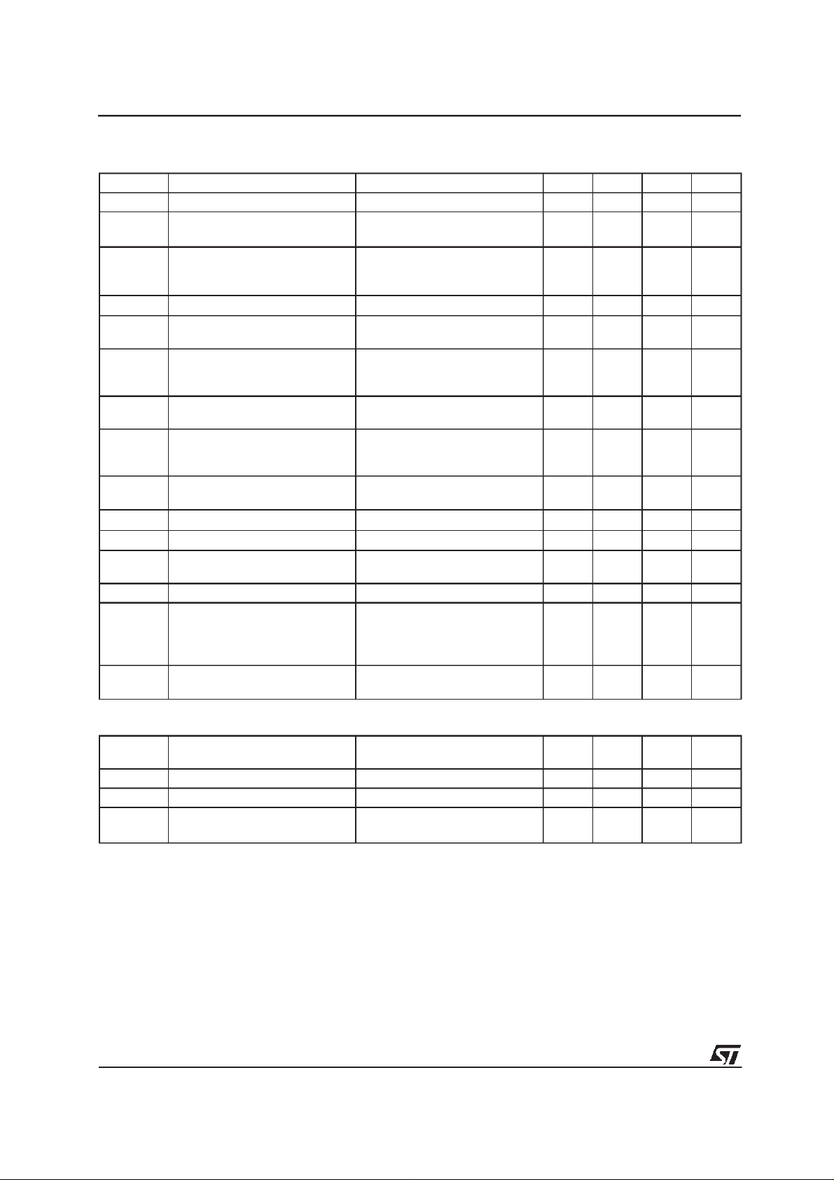
ELECTRICAL CHARACTERISTICS (VS= 14V; –40°C ≤ TJ≤ 125°C unlessotherwise specified)
Symbol Parameter Test Conditions Min. Typ. Max. Unit
V
V
V
O2-VO1
I
ADJ
V
DP1
V
V
DP2
V
V
OL 1.2
V
OLO1
V
OLO2
I
LIM1
I
LIM2
I
QSB
I
Operating Supply Voltage 25 V
S
StandbyOutput Voltage
O1
Output Voltage 2 TrackingError
(note 1)
6V ≤ V
1mA≤I
6V≤V
5mA≤I
≤ 25V
S
O1
≤
S
O2
50mA
≤
25V
500mA
≤
4.90 5.00 5.10 V
–25 +25 mV
Enable= LOW
ADJ InputCurrent IO1= 1mA; IO2= 5mA –1 0.1 1
DropoutVoltage 1 IO1= 10mA
Inputto OutputVoltage
IO1
I
= 50mA
O1
VS = 4V,IO1= 35mA 0.4 V
0.1
0.2
Differencein Undervoltage
Condition
DropoutVoltage 2 IO1 = 100mA
Inputto OutputVoltage
IO2
I
= 500mA
O1
VS = 4.6V,IO1= 350mA 0.6 V
0.2
0.3
Differencein Undervoltage
Condition
LineRegulation
6V ≤ V
I
Load Regulation 1
Load Regulation 2
1mA≤I
5mA≤I
Current Limit 1 VO1= 4.5V
V
≤ 25V
S
= 1mA; IO2= 5mA
O1
50mA
≤
O1
500mA
≤
O2
= 0V(note 2)
O1
55
25
100
50
Current Limit 2 VO2 = 0V 550 1000 1700 mA
Quiescent Current StandbyMode
(output2 disabled)
Quiescent Current IO1= 50mA
Q
I
= 0.3mA;TJ< 100°C
O1
2.4V
V
≥
EN
V
= 14V
S
V
= 3.5V
S
I
= 500mA
O1
210
340
0.25
0.4
0.3
0.6
20 mV
25 mV
50 mV
200
100
290
850
30 mA
µA
V
V
V
V
mA
mA
µ
µA
A
ENABLE
V
ENL
V
ENH
V
ENhyst
I
EN
4/12
EnableInput LOW Voltage
–0.3 1.5 V
(output2 active)
EnableInput HIGH Voltage 2.4 7 V
EnableHysteresis 30 75 200 mV
EnableInput Current 0V < VEN< 1.2V
2.5V < V
EN
<7V
–10–1–1.50–0.5
+1
µ
µ
A
A
 Loading...