

L4938E/ED
ADVANCEDVOLTAGE REGULATOR
ENABLE AND SENSE INPUTS (EN, SI) PROTECTED AGAINST NEGATIVE TRANSIENTS
DOWN TO-5V
RESET THRESHOLD ADJUSTABLE FROM
3.8 TO 4.7V
EXTREMELY LOW QUIESCENT CURRENT,
65µA (LESS THAN 90µA) IN STANDBY
MODE
OPERATINGDC SUPPLY VOLTAGE RANGE
5V -28V
OPERATING TRANSIENT SUPPLY VOLTAGE UP TO 40V
HIGHPRECISIONSTANDBYOUTPUTVOLTAGE 5V ± 1% WITH 100mA CURRENT CAPABILITY
OUTPUT 2 VOLTAGE 5V±2% WITH 400mA
CURRENT CAPABILITY (ADJ WIRED TO
V
)
OUT2
OUTPUT 2 VOLTAGE ADJUSTABLE BY EXTERNAL VOLTAGEDIVIDER
OUTPUT 2 DISABLE FUNCTION FOR
STANDBYMODE
L4938EPD
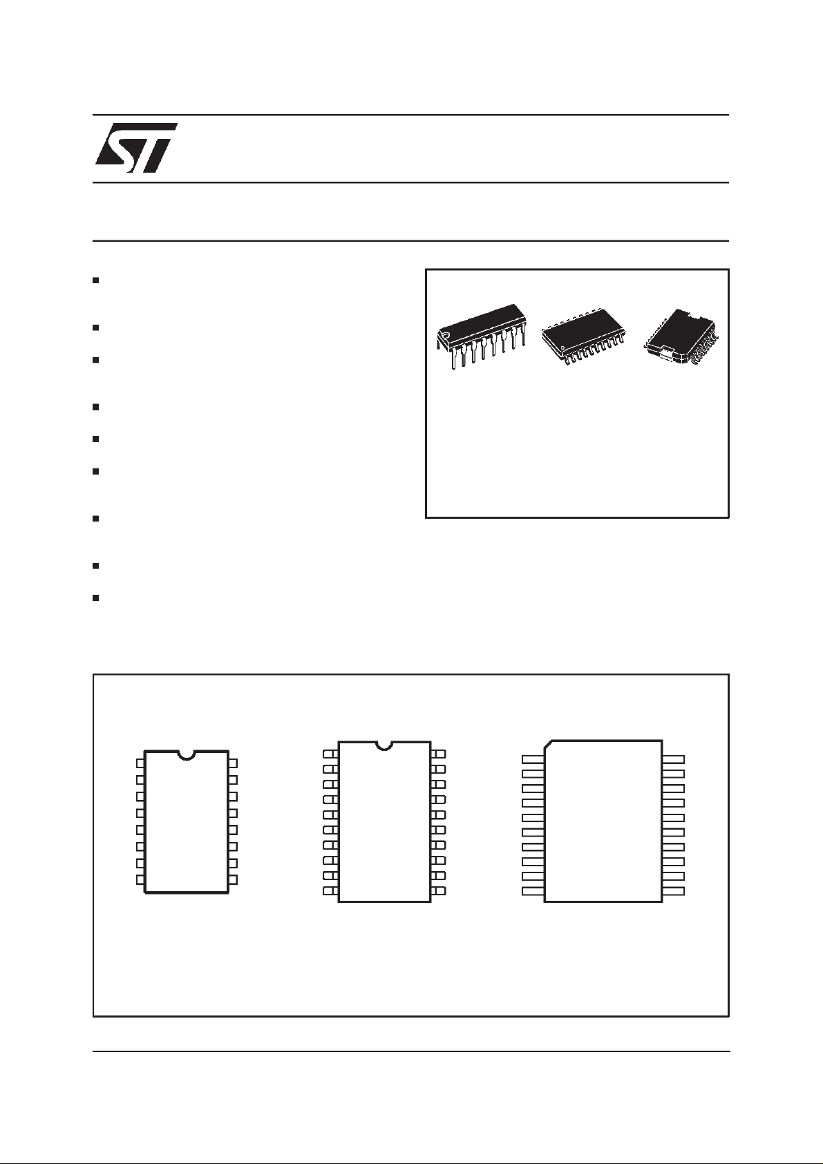
DIP (12+2+2) SO20 (12+4+4) PowerSO20
ORDERING NUMBERS:
DESCRIPTION
The L4938E/ED/EPD is a monolithic integrated
dual voltage regulator with two very low dropout
outputs and additional functions as power-on reset and input voltage sense. It is designed for
supplying the microcomputer controlled systems
especiallyin automotiveapplications.
L4938E (DIP)
L4938ED (SO)
L4938EPD (PSO)
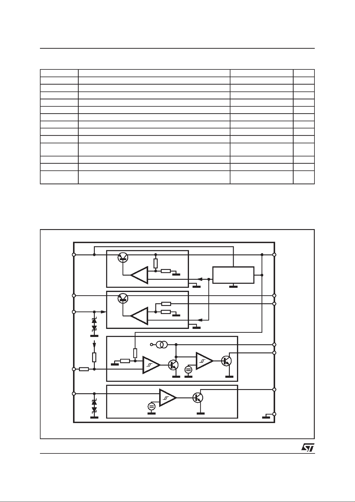
PIN CONNECTIONS
PR
1
CT
2
EN
3
GND
GND
RES
OUT1 8 ADJ9
4
5
6
SO
7 OUT2
D94AT075A
DIP (12+2+2)
February 1999
15
14
13
12
11
10
SI16
VS1
VS2
GND
GND
N.C.
PR
CT
EN
GND
GND
GND
GND
RES
SO OUT2
OUT1 ADJ
2
3
4
5
6
7
8
9
10
D94AT076A
SI1
20
VS1
19
VS2
18
GND
17
GND
16
GND
15
GND
14
N.C.
13
12
11
SO (12+4+4)
GND
N.C.
V
S2
V
S1
SI
PR
CT
EN
N.C.
GND 10
1
2
3
4
5
6
7
8
9
PowerSO20
L4938EPD
20
19
18
17
16
15
14
13
12
11
GND
N.C.
OUT2
ADJ
OUT1
SO
RESET
N.C.
N.C.
GND
1/12
L4938E - L4938ED - L4938EPD
ABSOLUTE MAXIMUM RATINGS
Symbol Parameter Value Unit
V
INDC
V
INTR
I
O
V
SI
I
SI
V
EN
I
EN
V
RES,VSO
I
RES,ISO
P
O
T
stg
T
j
T
JSD
Note 1: The circuit is ESDprotected according to MIL-STD-883C
Note 2: Current forcedmeans voltage unlimited but current limited to the specified value
Voltageforced means voltage limitedtothe specified valueswhile the current is not limited
Note 3: Typicalvalue soldered on a PC board with 8cm
DC Operating Supply Voltage 28 V
Transient Operating Supply Voltage (T < 400ms) -14 to 40 V
Output Current internally limited
Sense Input Voltage (VoltageForced) (note 2) -20 to 20 V
Sense Input Current (Current Forced) (note 2)
1mA
±
Enable Input Voltage(Voltage Forced) (note 2) -20 to 20 V
Sense Input Current (Current Forced) (note 2)
1mA
±
Output Voltages -0.3 to 20 V
Output Currents (Output Low) 5 mA
Power Dissipation at T
=80°C (note 3)
amb
875 mW
Powerdip 12+2+2
Storage Temperature -65 to 150 °C
Operating Junction Temperature -40 to 150
Thermal shutdownjunction temperature Output 2 will shut-down
165
typically at Tj 10K lowerthan output 1
2
copperground plane (35mm thick).
C
°
C
°
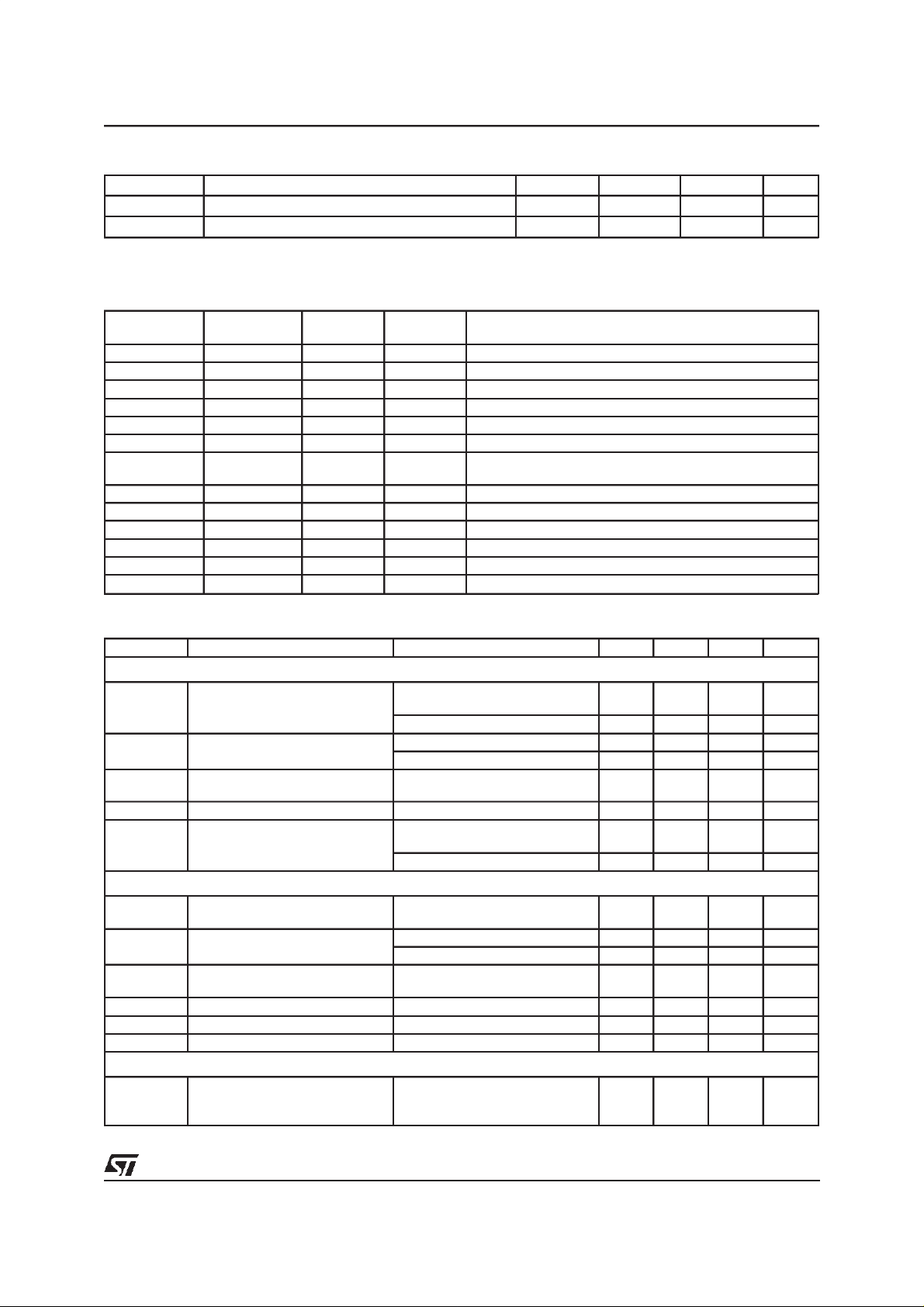
BLOCK DIAGRAM
VS1
VS2
EN
1.23V
PR
SI
REG1
REG2
RESET
OUT1
1.23V REFERENCE
OUT2
ADJ
1.23V
CT
RES
1.4V
SO
2/12
SENSE
1.23V
GND
D94AT074A
L4938E - L4938ED - L4938EPD
THERMAL DATA
Symbol Parameter DIP 12+2+2 SO 12+4+4 PowerSO20 Unit
R
th j-amb
R
th j-case
Note 3: Typicalvalue soldered on a PC board with 8cm2copperground plane (35mm thick).
PIN FUNCTIONS
Thermal ResistanceJunction to ambient 40 50 Thermal ResistanceJunction to case - - <2 °C/W
C/W
°
PIN
(DIP 12+2+2)
PIN
(SO 12+4+4)
PIN
PowerSO20
Name Function
14 18 3 VS2 Supply Voltage (400mA Regulator)
15 19 4 VS1 Supply Voltage (100mA Regulator, Reset, Sense)
16 20 5 S1 Sense Input
1 1 6 PR Reset Theresold Programming
2 2 7 CT Reset Delay Capacitor
3 3 8 EN Enable (low willactivate the 400mA regulator)
4, 5, 12, 13 4, 5, 6,7, 14,
1,10,11,20 GND Ground
15, 16, 17
6 8 14 RES Reset Output
7 9 15 SO Sense Output
8 10 16 OUT 1 100mA Regulator Output
9 11 17 ADJ Feedback of 400mA Regulator
10 12 18 OUT 2 400mA Regulator Output
11 13 2,9,19 NC Not Connected
ELECTRICALCHARACTERISTICS
= 14V; Tj=-40 to 150°C unless otherwise specified.)
(V
S
Symbol Parameter Test Condition Min. Typ. Max. Unit
OUT 1
V
V
V
V
I
O1
DP1
OL01
LIM1
QSB
Supply Output Voltage VS= 6 to 28V;
I
= 400µA to 100mA
O1
125°C; I
T
≤
Dropoutput Voltage 1 I
Load Regulation 1 I
j
OUT1
I
OUT1
OUT1
O1
= 10mA 0.1 0.2 V
= 100mA; VS= 4.8V 0.2 0.4 V
= 1 to 100mA
= 50 to 400µA 4.8 5 5.2 V
4.9 5 5.1 V
25 mV
(after regulation setting)
Current Limit 1 VOUT1 = 0.8 to 4.5V 100 200 400 mA
Quiescent Current in Standby
Mode
2.4V (output 2 disabled)
I
≥
EN
I
= 0.1mA; VSI> 1.3V
O1
<85°C;RPR=0 75 µA
T
J
65 90
OUT 2
V
V
V
R
I
O2
DP2
OL02
ADJ
LIM2
I
Q
Output Voltage 2
ADJ connected to OUT 2
Dropoutput Voltage 2 I
Load Regulation 2 I
Enable = LOW;VS= 6 to 28V;
I
= 5 to 400mA
02
= 100mA 0.2 0.3 V
OUT2
= 400mA; VS= 4.8V 0.3 0.6 V
I
OUT2
= 5 to 400mA
OUT1
4.9 5.1 V
50 mV
(after regulation setting)
Adjust Input Resistance 60 100 150 mA
Current Limit 2 V02 = 0.8 to 4.5V 450 650 1300 mA
Quiescent Current I
OUT1
= 100mA; I
= 400mA 20 mA
OUT2
OUT1,OUT 2
V
OLi 1,2
Line Regulation VS= 6 to 28V; IO1= 1mA,
I
= 5mA,
O2
(after regulation setting)
20 mV
A
µ
3/12
L4938E - L4938ED - L4938EPD
ELECTRICALCHARACTERISTICS
(Continued)
Symbol Parameter Test Condition Min. Typ. Max. Unit
ENABLE INPUT
V
ENL
V
ENH
V
ENhyst
I
EN LOW
I
EN HIGH
Enable Input Low Voltage
-20 1 V
(Output 2 Active)
Enable Input High Voltage 1.4 20 V
Enable Hysteresis 20 30 60 mV
Enable Input Current Low VEN= 0 -20 -8 -3 µA
Enable Input Current High VEN= 1.1 to 7V; TJ< 130°C; -1 0 1 µA
= 1.1 to 7V;
V
EN
T
= 130 to 150°C;
J
-10 0 10 µA
RESETCIRCUIT
V
RT
V
RTH
t
RD min
t
RD nom
t
RR
I
CT
I
CT
V
RESL
V
RESH
Reset Theresold Voltage
(note4)
Reset Theresold Hysteresis RPR=
Reset Pulse Delay C
Reset Pulse Delay C
Reset Reaction Time C
Pull Down Capability of the
RPR= ∞ 4.5 VO1-0.3 VO1-0.2 V
= 0 3.65 3.8 3.95 V
R
PR
∞
= 47nF; t
RES
= 47nF; (note 6) 60 100 140 ms
RES
= 47nF 10 50 150 µs
RES
V
OUT1<VRT
s; (note 5) 40 60 100 ms
≤30µ
r
30 60 120 mV
3615mA
Discharge circuit
Charge Current VOUT1 >VRT -1.3 -1 0.7 µA
Reset Output Low Voltage RRES = 10KΩ to VOUT1
1.5V
OUT1 ≥
=5V 1 µA
RES
Reset Output High Leakage
V
V
0.4 V
current
SENSECOMPARATOR
V
SI
V
SIT
V
SITH
V
SOL
I
SOH
I
SI HIGH
I
SI LOW
Note :
4) The reset threshold can be programmed continuously from typ 3.8V to 4.7V by changinga value of an external resistor frompin PR to GN
5) This is a minimum reset timeaccording to thehysteresis of the comparator. Delay timestarts with V
6) This is thenominal reset timedepending on the discharging limit of CT(saturationvoltage) and theupper threshold of the timer comparator.
Delay time starts with V
7) The leakage of CTmust be less than0.5mA (2V). If an externalresistor between CT and VOUT1is applied, the leakage current may be
increased. The external resistor should have more than 30KΩ.
for stability: Cs ≥ 1µF, C01 ≥ 10µF, C02 ≥ 10µF, ESR ≤ 5Ω (designed target) For details see application note.
8) For transients exceeding 20V or -20V externalprotection is required at the Pins SIand EN as shown at Pin EN. The protectionproposed will
provide proper function for transients in the range of ±200V. If the zener diode is omitted the external resistor should be raised to 200KΩ
to limit the current to 1mA. Without the zener diode, the function 20V or -20Vcan not be guaranteed.
Functional Range -20 20 V
Sense Threshold Voltage Falling Edge; TJ<130°C 1.08 1.16 1.24 V
Falling Edge; T
<130 to 150°C 1.05 1.16 1.29 V
J
Sense Threshold Hysteresis 10 30 60 mV
Sense Output Low Voltage VSI≤ 1.05V; RSO=10KΩ
connected to 5V; V
Sense Output Leakage VSO= 5V; V
SI ≥
5V
S ≥
1.5V 1
0.4 V
A
µ
Sense Input Current High VSI= 1.1 to 7V; TJ<130°C-101µA
= 1.1to 7V; TJ<130 to150°C -10 0 10 µA
V
SI
Sense Input Current Low VSI= 0V -20 -8 -3 µA
OUT1 exceeding VRT
OUT1
exceeding V
RT
4/12
 Loading...