

VERY LOW DROPREGULATOR WITHRESET
.VERY LOW DROP (max. 0.9 V at 1 A) OVER
FULLOPERATINGTEMPERATURERANGE
(– 40 / + 125°C)
.LOW QUIESCENT CURRENT (max 70 mA at
1 A)OVERFULLT RANGE
.PRECISE OUTPUT VOLTAGE (5 V ± 4%)
OVERFULLT RANGE
.POWER ON-OFF INFORMATION WITH SET-
TABLEDELAY
.REVERSEBATTERYPROTECTION
.
SHORTCIRCUIT PROTECTION
.THERMALSHUTDOWN
L4922
Pentawatt
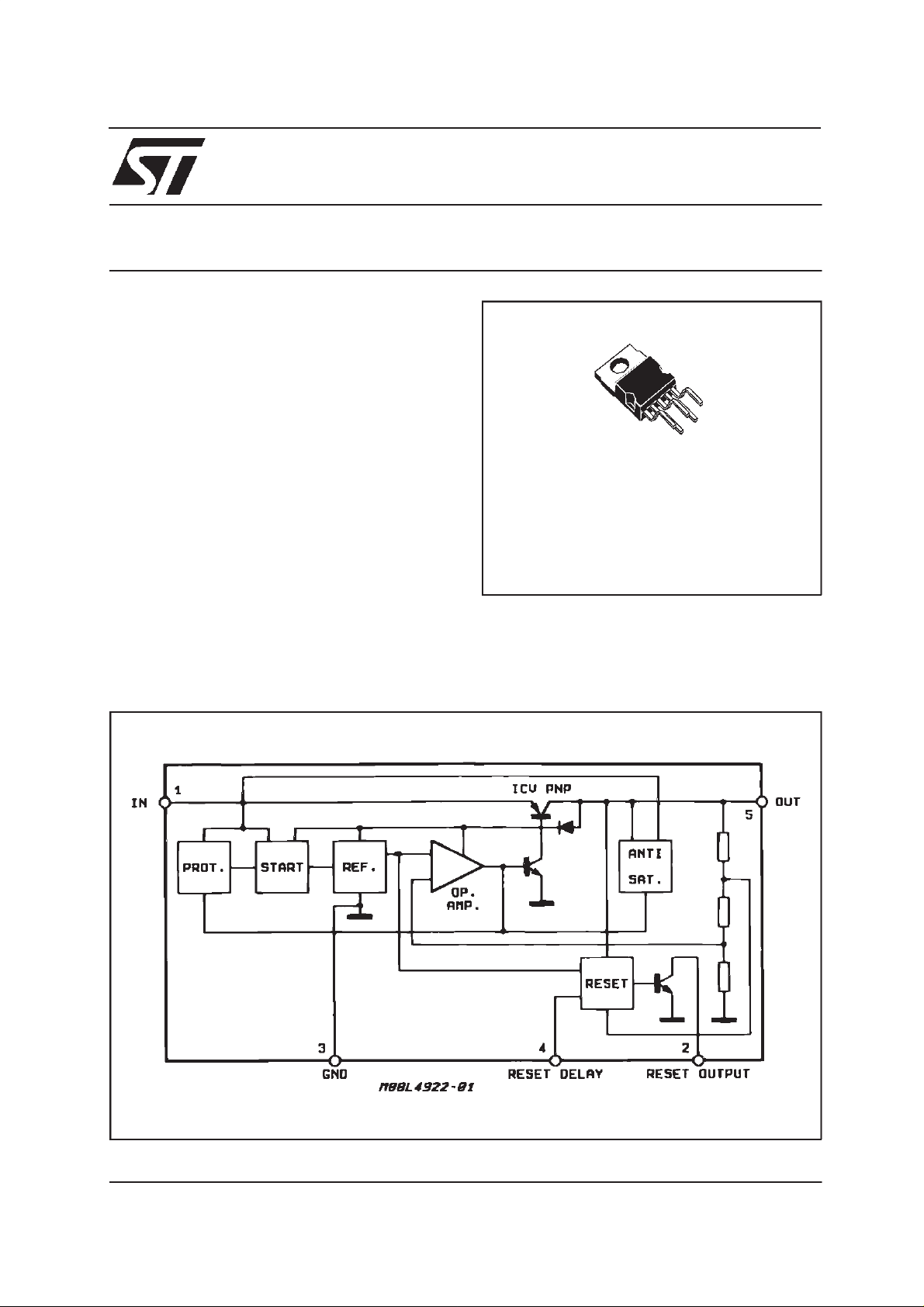
DESCRIPTION
TheL4922isahighcurrentmonolithicvoltageregulatorwith verylow voltagedrop (0.70V max at 1 A,
=25°C).
T
J
The device is internally protected against load
dumps transient of + 60V, reverse polarity, over-
BLOCK DIAGRAM
ORDERING N UM B E R : L4922
heatingandoutputshortcircuit :thankstotedforthe
automotiveand industrialapplications.
June 2000
This is advanced informationona new product now in development or undergoing evaluation. Detailsare subjectto changewithout notice.
1/6
L4922
ABSOLUTEMAXIMUM RATINGS
Symbol Parameter Value Unit
V
V
V
T
T
T
Note: T he circuit is ESD protected according to MIL-STD-883C
THERMAL DATA
Symbol Parameter Value Unit
R
th j-case
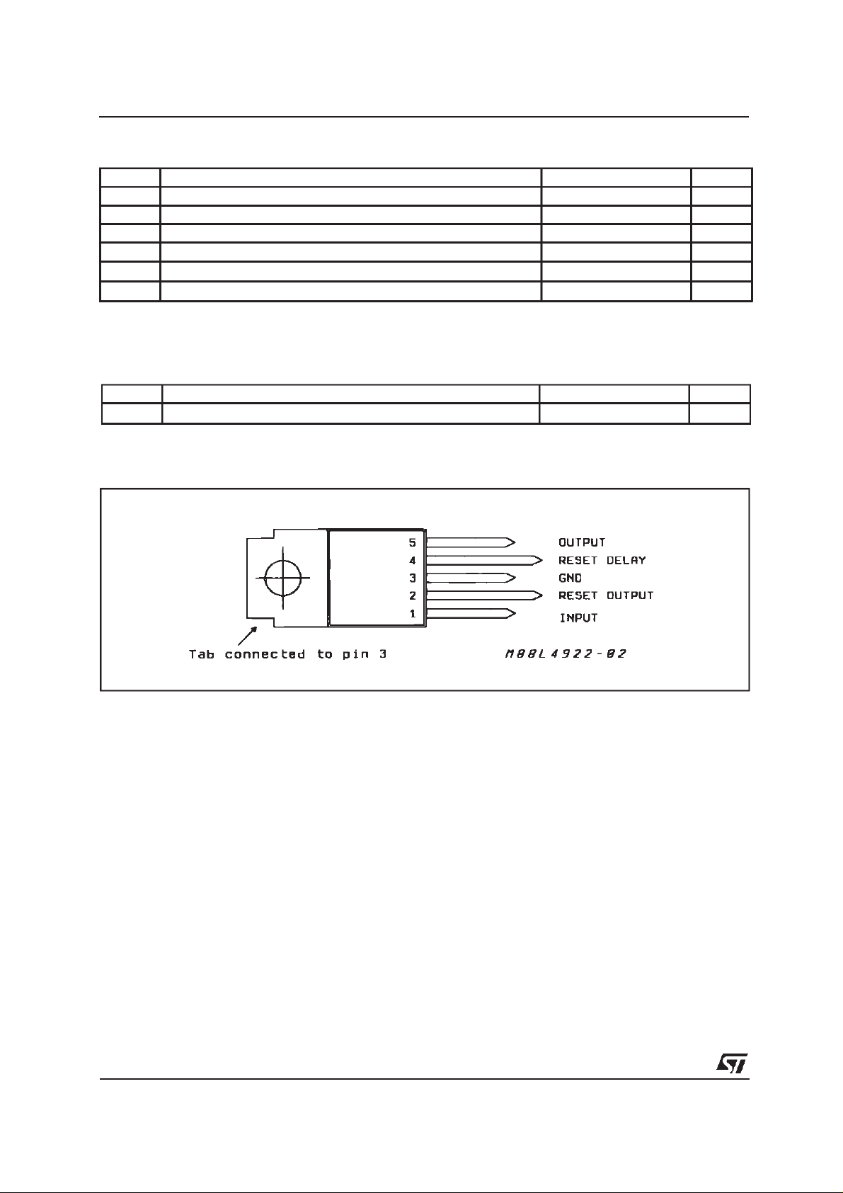
PIN CONNE CTIO N (Top view)
DC Input Voltage 35 V
i
DC Reverse Voltage –18 V
r
Positive Load Dump Protection (t = 300ms) 60 V
D
Junction Temperature Range –40 to 150 °
J
Operating Temperature Range –40 to 125 °
op
Storage Temperature Range –55 to 150
stg
Thermal Resistance Junction-case Max. 3.5
°
C
C
C
°
C/W
FUNCTI O NAL DESCRI PTION
The operatingprinciple of the voltage regulator is
basedonthereference,theerroramplifier,thedriver
and the power PNP. This stage uses an Isolated
CollectorVerticalPNPtransistorwhich allowsto obtainvery low dropoutvoltage(typ. 450mV)and low
quiescentcurrent(I
= 20mA typicallyatIo= 1A).
Q
Thanks to these featuresthe device is particularly
suited when the power dissipation must be limited
as,for example,in automotiveor industrialapplicationssuppliedby battery.
The three gain stages (operational amplifier,
driverand powerPNP) requiretheexternalcapacitor (Co
=22µF) to guaranteethe global stability
min
of the system.
2/6
Theantisaturationcircuitallowstoreducedrastically
the currentpeak whichtakes place during the start
up.
The reset function is LOW active when the output
voltagelevel islower than the resetthreshold voltageV
putvoltageis higherthanV
(typ.value:Vo–150mV).Whentheout-
RthOFF
theresetbecomes
RthON
HIGHafteradelaytimesettablewiththeexternalcapacitorC
.Typicallytd=20ms,Cd=0.1µF.Thereset
d
and delay threshold hysteresis improve the noise
immunity allowing to avoid false switchings. The
typicalresetoutputwaveformis shownin fig. 1.
 Loading...