

DUAL 5V REGULATOR WITH RESETAND DISABLE
.
DOUBLEBATTERYOPERATING
.
OUTPUTCURRENTS : I01=300 mA
= 300 mA
I
02
.
FIXED PRECISIONOUTPUT VOLTAGE
5V±
2
%
.
RESETFUNCTION CONTROLLED BY INPUT
VOLTAGEANDOUTPUT1 VOLTAGE
.
RESET FUNCTION EXTERNALLY PROGRAMMABLETIMING
.
RESET OUTPUT LEVEL RELATED TO OUTPUT 2
.
OUTPUT 2 INTERNALLY SWITCHED WITH
ACTIVEDISCHARGING
.
OUTPUT2 DISABLELOGICALINPUT
.
LOW LEAKAGE CURRENT, LESS THAN 1µA
ATOUTPUT1
.
RESETOUTPUT NORMALLY HIGH
.
INPUT OVERVOLTAGE PROTECTION UP TO
60V
.
OUTPUTTRANSISTORS SOA PROTECTION
.
SHORT CIRCUIT AND THERMAL OVERLOADPROTECTION
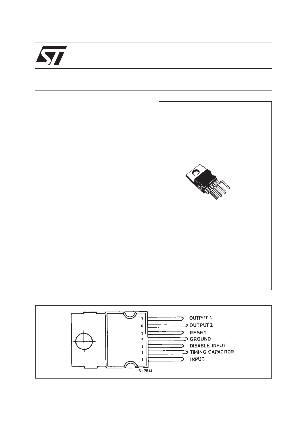
L4902A
HEPTAWATT
ORDERING NUMBER : L4902A
(Vertical)
DESCRIPTION
The L4902A is a monolithic low drop dual 5V
regulatordesignedmainlyfor supplying microprocessorsystems.
Reset and data save functions and remoteswitch
on/offcontrol can be realized.
PIN CONNECTION
June 2000
1/9
L4902A
PIN FUNCTIONS
N°
1 Input 1 Regulators Common Input
2 Timing
3 Disable Input A high level (> V
4 GND Common Ground
5 Reset Output When pin 2 reaches 5V the reset output is switched high.
6 Output 2 5V – 300mA Regulator Output. Enabled if V
7 Output 1 5V – 300mA. Low leakage (in switch-OFF condition) output
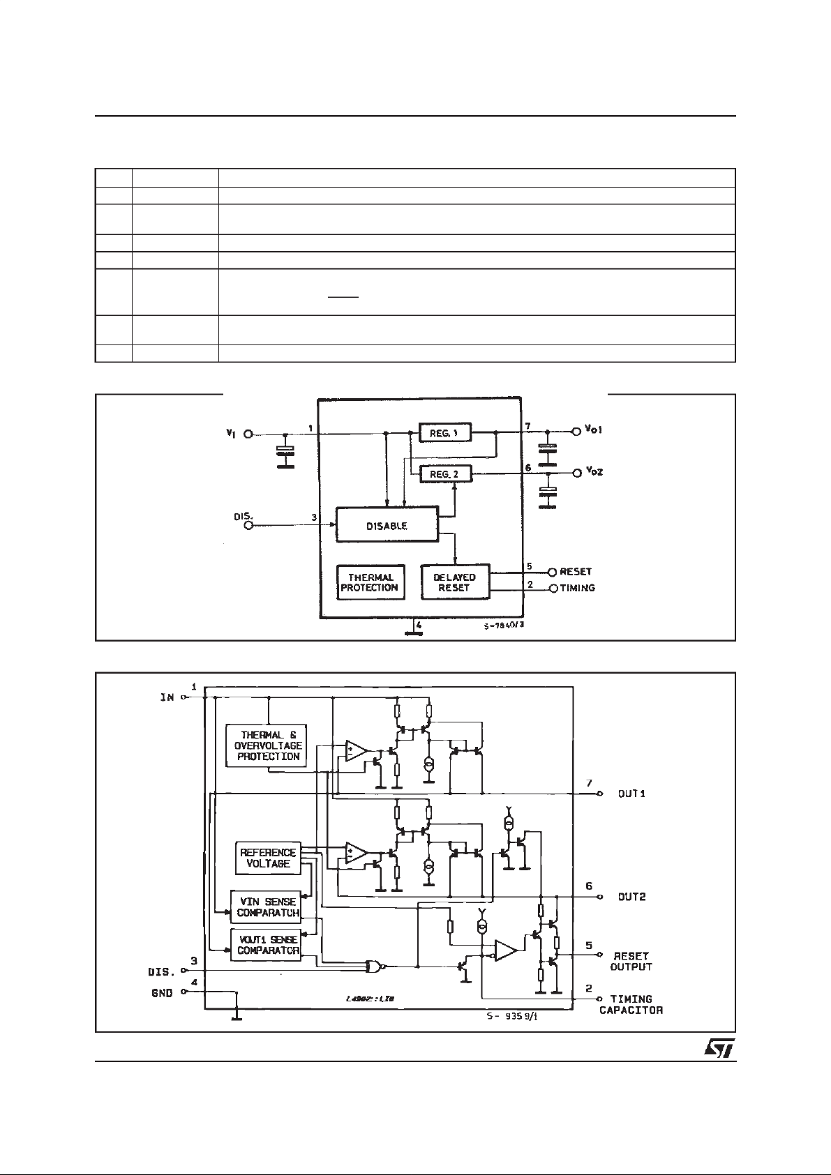
BLOCKDIAGRAM
Name Function
If Reg. 2 is switched-ON thedelay capacitor is charged with a5µA constant current. When
Capacitor
Reg. 2 is switched-OFF the delay capacitor is discharged.
) disable outputReg. 2.
DT
5V
(
Therefore t
RD=Ct
Reg. 2 is switched-OFF the C
);tRD(ms) = Ct(nF)
10µA
capacitor is discharged.
02
1>VRT. DISABLE INPUT < VDTand VIN>VIT.If
o
SCHEMATIC DIAGRAM
2/9
L4902A
ABSOLUTE MAXIMUMRATINGS
Symbol Parameter Value Unit
V
I
T
stg,Tj
IN
o
DC Input Voltage
Transient Input Overvoltage(t = 40ms)
Output Current Internally Limited
Storage and Junction Temperature – 40 to 150
THERMAL DATA
Symbol Parameter Value Unit
R
th j-case
Thermal Resistance Junction-case Max 4
28
60
V
V
°C
°C/W
ELECTRICAL CHARACTERISTICS
(V
IN
= 14.4V,T
=25oC unless otherwise specified))
amb
Symbol Parameter Test Conditions Min. Typ. Max. Unit
V
DC Operating Input Voltage 24 V
i
V
V
V
I
I
L01
I
V
V
V
∆V
∆V
∆V
∆V
V
V
V
V
t
V
∆V
∆
∆V
∆
SVR1 Supply Voltage Rejection f = 100Hz V
Output Voltage 1
01
Output Voltage 2 HIGH
02 H
Output Voltage 2 LOW I02= – 5mA 0.1 V
02 L
Output Current 1 max.
01
Leakage Output 1 Current
Output Current 2 max.
02
Output 1 Dropout Voltage (*) I01= 10mA
i01
Input Threshold Voltage V01+ 1.2 6.4 V01+ 1.7 V
IT
Input Threshold VoltageHyst. 250 mV
iTH
Line Regulation 1 7V < VIN< 24V,I01= 5mA 5 50 mV
01
Line Regulation 2 7V < VIN< 24V,I02= 5mA 5 50 mV
02
Load Regulation 1 5mA < I01< 300mA 40 80 mV
01
Load Regulation 2 5mA < I02< 300mA 50 80 mV
02
Quiescent Current
I
Q
Reset Threshold Voltage V02– 0.15 4.9 V02– 0.05 V
RT
Reset Threshold Hysteresis 30 50 80 mV
RTH
Reset Output Voltage HIGH
RH
Reset Output Voltage LOW IR= – 1mA 0.25 0.4 V
RL
Reset Pulse Delay Ct= 10nF 3 5 11 ms
RD
t
Timing Capacitor Discharge Time Ct= 10nF 20
d
V02Disable Threshold Voltage 1.25 2.4 V
DT
I
V02Disable Input Current
D
01
Thermal Drift
T
02
Thermal Drift
T
R Load 1k
R Load 1k
= – 100mV
∆V
01
=0,V01≤ 3V
V
IN
= – 100mV
∆V
02
= 100mA
I
01
= 300mA
I
01
I
0<V
7V < V
7V < V
I
V
V
01=I02
= 500µA
R
≤ 0.4V
D
≥ 2.4V
D
≤
< 13V
IN
< 13V V02LOW
IN
< 13V V02HIGH
IN
–20°C≤T
–20°C≤T
Io = 100mA
Ω 4.95 5.05 5.15 V
Ω V
–0.1 5 V
01
300 mA
300 mA
0.7
0.8
1.1
5mA
4.5
2.7
1.6
V
– 1 4.12 V
02
– 150
–30
amb
amb
R
≤125°C
≤125°C
= 0.5V
50 84 dB
0.3
– 0.8
0.3
– 0.8
1
0.8
1
1.4
6.5
4.5
3.5
01
V
µA
V
V
V
mA
02
V
µs
µA
µA
mV/°C
mV/°C
SVR2 Supply Voltage Rejection 50 80 dB
* The dropoutvoltage is defined as thedifference between theinput and the outputvoltage when theoutputvoltage is lowered of 25mV under
constant output current condition.
3/9
 Loading...