

L484
MAGNETIC PICKUP IGNITIONCONTROLLER
.DIRECT DRIVING OF THE EXTERNAL DAR-
LINGTON
.OPERATES WITH A WIDE RANGE OF MA-
GNETIC PICKUPTYPES
.CHARGINGANGLE(DWELL) CONTROL
.COILCURRENT PEAKLIMITATION
.CONTINUOUSCOILCURRENTPROTECTION
.TACHOMETER SIGNALOUTPUT
.EXTERNAL DARLINGTON OVERVOLTAGE
PROTECTION
.LOAD DUMP ANDREVERSEBATTERYPRO-
TECTION
.POSSIBILITY OF SPARK POINT DELAYING
(ANTIKNOCKSYSTEM)
DESCRIP TIO N
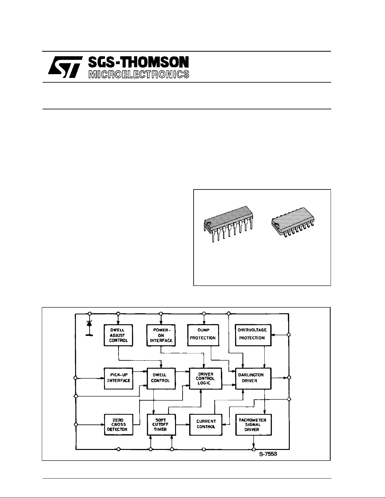
The L484 is an integratedcircuit designed for use
with an NPN darlington in breakerlessignition systemswithmagneticpickupsensorsand high energy ignitioncoils.
A keyfeatureofthe L484isflexibility.It canbeused
withawidevarietyof magneticsensorsthankstothe
BLOCK DIAGRAM
specialdesignwhichhastwoinputpinsfromthepickup ; the first is the zero crossing detector for the
ignitioncommandandthesecondpinisusedtocalculatethe dwelltime. Moreoveranotherpin is used
to adapt the L484 to variouspickup types.
Otherfeaturesof thedeviceincludedarlingtonovervoltageprotection,dump protection, a supply voltage rangeof 6-28 V.
DIP16
ORDERING NUMBERS : L484 (DIP16)
L484D1 (SO16)
SO16
November 1991
1/11
L484
ABSOLUTEMAXIMUM RATINGS
Symbol Parameter Value Unit
V
V
P
T
j,Tstg
PIN CONNECTION
Reverse Battery Voltage – 14 V
R
Dump Voltage 100 V
D
Power Dissipation at T
tot
=90°C 0.75 W
amb
Junction and Storage Temperature Range – 55 to 150 °C
THERMAL DATA
Symbol Parameter Value Unit
Thermal Resistance Junction-ambient (DIP16) Max 80 °C/W
Thermal Resistance Junction-alumina (SO16) Max 50 °C/W
2/11
R
th j-amb
R
th j-al
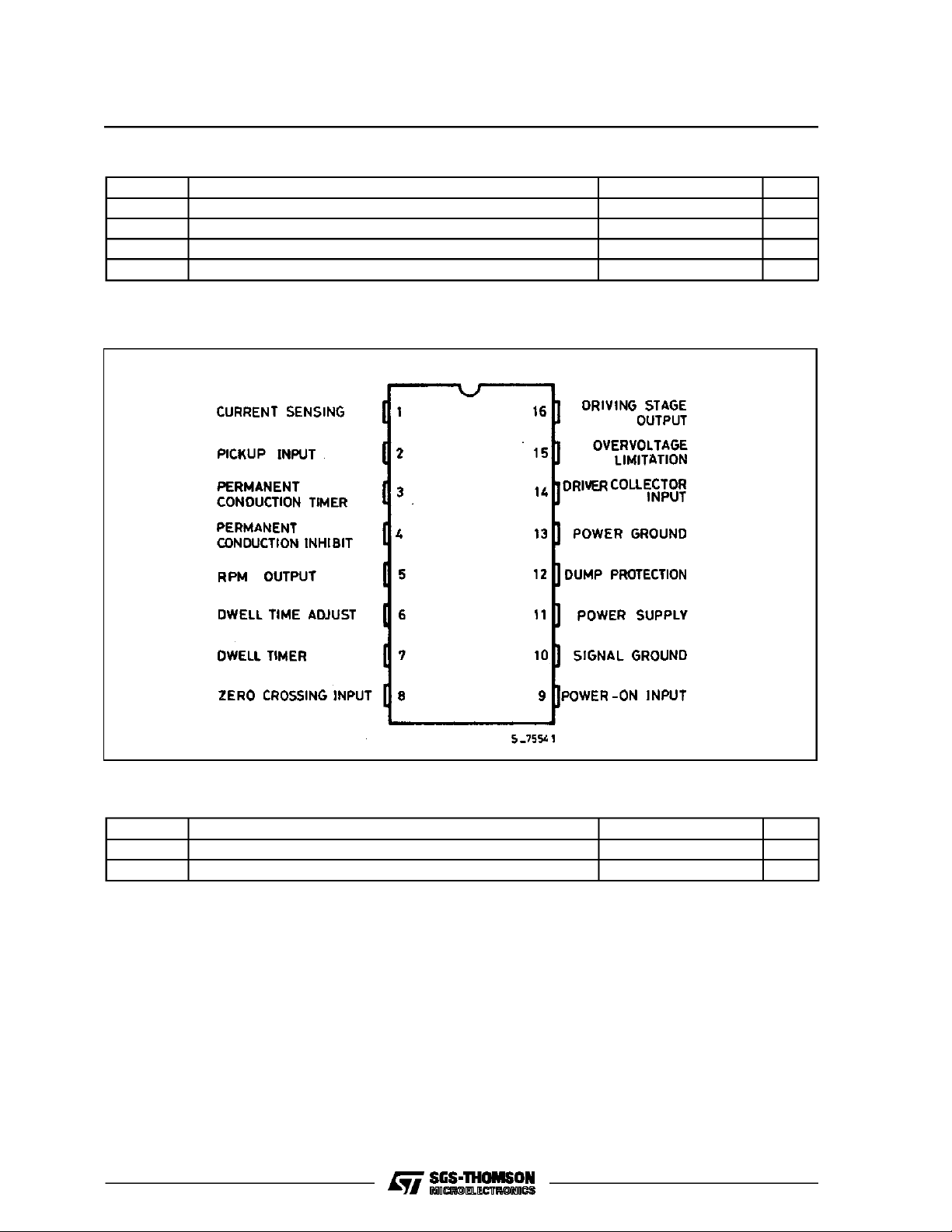
PINFUNCTIONS (refer to fig. 2)
N° Name Function
1 CURRENT SENSING
INPUT
2 PICKUP INPUT Magnetic Pickup Signal Input. This pin sets the dwell time, i.e. the max
3 PERMANENT
CONDUCT.
PROTECTION TIMER
4 PERMANENT CONDUCT.
PROTECTIONINHIBIT
5 RPM OUTPUT Open collector output signal which is at a low level when the final darlington
6 DWELL TIME ADJUST At high motor rotation speeds, i.e. when the peak value of the magnetic
7 DWELL CONTROL
TIMER
8 ZERO CROSSING
INPUT
9 POWER-ON INPUT A low level on this pin forces the external darlington into conduction
10 SIGNAL GROUND This pin must be connected to ground.
11 POWER SUPPLY Supply Voltage Input. A 7V (typ) zener is present at the input. The external
12 DUMP PROTECTION The device is protected against the load dump. In load dump condition an
Connection for Coil Current Limitation. The current is measured on the
sense resistor R
and divided on R1/R2. The current limitation value is
SENS
given by :
SENS
R
SENS
R2
R1 + R2
=
I
negative pickup voltage value starting from which the device can drive the
current into the coil. The real dwell time will be a function of the dwell
control logic. Increasing the resistor R11 the maximum conduction time
increases. The max input current foreseen is 2mA.
A capacitor C1 connected between this pin and ground sets the delay of the
permanent conduction protection in the coil current. Using a 50nF capacitor
the typical desaturation time delay for the protection is 75ms.
A low level on this input (max 0.7V) disables the protection, irrespective of
the state of pin 3. If the protection is used this pin must be left open.
is in ON status. The current is internally limited at 10mA.
pick-up signal exceedes 6V using R12 = 100KΩ, this pin may be used to
vary the dwell ratio. Adding a resistor in series R
between this pin and pin
a
11 the desaturation time is reduced. It is therefore possible to use this pin to
adapt the L484 to various pickup types. The maximum value of the resistor
is 200KΩ.
R
a
A capacitor C2 connected between this pin and ground sets the timing for
the dwell control. The recommended value is 100nF. The resistors R
provide an hysteresis to confirm ON state and avoid spurious sparks.
Zero cross detector input of the magnetic pickup signal for the ignition
actuation. At high motor rotation speeds, the external resistor R12 may be
used to vary the desaturation time ratio, to adapt the L484 to various
signal waveforms of time magnetic pick-up. Reducing the resistor value the
dwell time increases. Typically the range of values for resistor R12 is from
50KΩ to 150KΩ..
particularly useful in anti knock system. This function is particularly useful in
antiknock system because provides a spark time delay. Anyway the current
limitation, the permanent conduction protection and the dump protection
are operating even when pin 9 is at a low level. If this function is not used it
must be left open.
resistor R9 limits the current through the zener for higher supply voltages.
internal circuit, based on a zener diode and a darlington transistor,
switches off the external darlington and short circuits the supply.
By means of the external divider R8/R9 the protection threshold can be
changed and is given as first approximation by:
L484
b/Rc
Dth
R8+ R9
= 8.5
V
R9
+ 5 ⋅ 10
−4
R8
(the resistor R9 value must be higher than 4KΩ).
13 POWER GROUND This pin must be connected to ground.
* this function is particularly useful in antiknocksysteme because provides a spark time delay. anywaythe current limitation,the pemanent con
ductionprotection and the dump protectionare operating even when pin 9 is at a low level.
3/11
L484
PINFUNCTIONS (continued)
N° Name Function
14 DRIVER COLLECTOR
INPUT
15 OVERVOLTAGE
LIMITATION
The collector current for the internal driver which drives the external
darlington is supplied through this pin. The external resistor R10 limits the
dissipation in the IC. The value this resistor depends on the darlington used
and on the limiting current in the coil.
The external darlington is protected against overvoltage by means of an
internal zener available at this pin. The external divider R5/R6 defines the
limitation value, typically given by :
30
+ 5 ⋅ 10
=
V
ovp
R5
−3
⋅
R6+ 30
16 DRIVING STAGE
OUTPUT
Current Driver for the External Darlington. To ensure stability on the current
limitation loop a capacitor C3 (typically 2.2nF, this value depending on the
darlington used) must be connected between this pin and the current
sensing input (pin 1).
ELECTRICAL CHARACTERISTICS (VS=14.4V ; TJ=- 40 to 125°C unlessotherwisespecified ; referred
to the test circuit)
Symbol Parameter Test Conditions Min. Typ. Max. Unit
V
V
V
V
SENS
V
V
I
I
I7D/I
I
I
TH
ZC
7C
7D
7C
7D
Operating Supply Voltage 6 28 V
S
Input Stage Voltage (pin 2 with
IS
160 200 240 mV
10KΩ resistor)
On Pick-up Thresh. Voltage at LOW RPM
VIS–30 VIS+30 mV
(pin 2)
Current Limitation Sensing Voltage (pin 1) VS= 6 to 16V 200 320 mV
Zero Crossing Thresh. Voltage (pin 8) 3 20 60 mV
Hysteresis Voltage (pin 8) 100 200 mV
H
C
D WELL
C
D WELL
Charge Current
Discharge Current
at LOW RPM
V
= 0.5V ;
pick-up
0.7
7
or pin 6 notconnected
7C
C
C
Charge Current
D WELL
Discharge Current
D WELL
(*) Note 1
at HIGH RPM
V
=9V
pick-up
7
8
13
30
15
33
44
3
µA
µA
µA
µA
4/11
I7D/I
V
V
V
V
pin3
I
3
V
Cp
CEsat
V
Z
OVZ
I
09
CH
I
CH
7C
Threshold Voltage
Output Current
Continuous Coil Current Protection Inhibit
(**) Note 2
T
=25°C
amb
(***) Note 3
0.7
0.85 4
0 0.7 V
LOW Voltage (pin 4).
Series Darlington Driver
Saturation Voltage (V
pin14 - 16
)
Zener Volt. Pin 11 I
External Darlington Overvoltage Protection
Zener Voltage
I
= 150mA
pin14
= 50mA
I
pin14
= 140mA 6.5 8.8 V
pin11
T
I
pin15
amb
=25°C;
= 5 to 15mA
25 35 V
0.4 1
Pin 9 Output Current in Low Status V9=0V 3 mA
Tachometer Signal Output LOW Voltage.
(pin5)
Output Leakage (pin 5)
ON Condition
= 0.5mA
I
sink
OFF Condition
=5V
V
pin5
3.2
3
0.6
0.7
10
V
µA
V
V
V
µA
 Loading...