HALL–EFFECT PICKUP IGNITION CONTROLLER
.DIRECT DRIVING OF THE EXTERNAL PO-
WERDARLINGTON
.COILCURRENT CHARGING ANGLE(DWELL)
CONTROL
.COILCURRENT PEAK VALUELIMITATION
.CONTINUOUSCOILCURRENTPROTECTION
.CONDUCTION AND DESATURATION TIME
OUTPUT SIGNALS
.PERMANENT CONDUCTION PROTECTION
RESETOUTPUTSIGNAL
.OVERVOLTAGE PROTECTION FOR EXTER-
NALDARLINGTON
.LOADDUMP PROTECTION
L482
DIP16
DESCRIP T IO N
The L482 is an integratedcircuit designed foruse
with an NPN darlington in breakerlessignition systemswithhall-effectpickupsensorsandhighenergy ignitioncoils.
It controls the energy stored in the ignition coil and
the desaturation time of the external darlingtonto
limit the power dissipation.
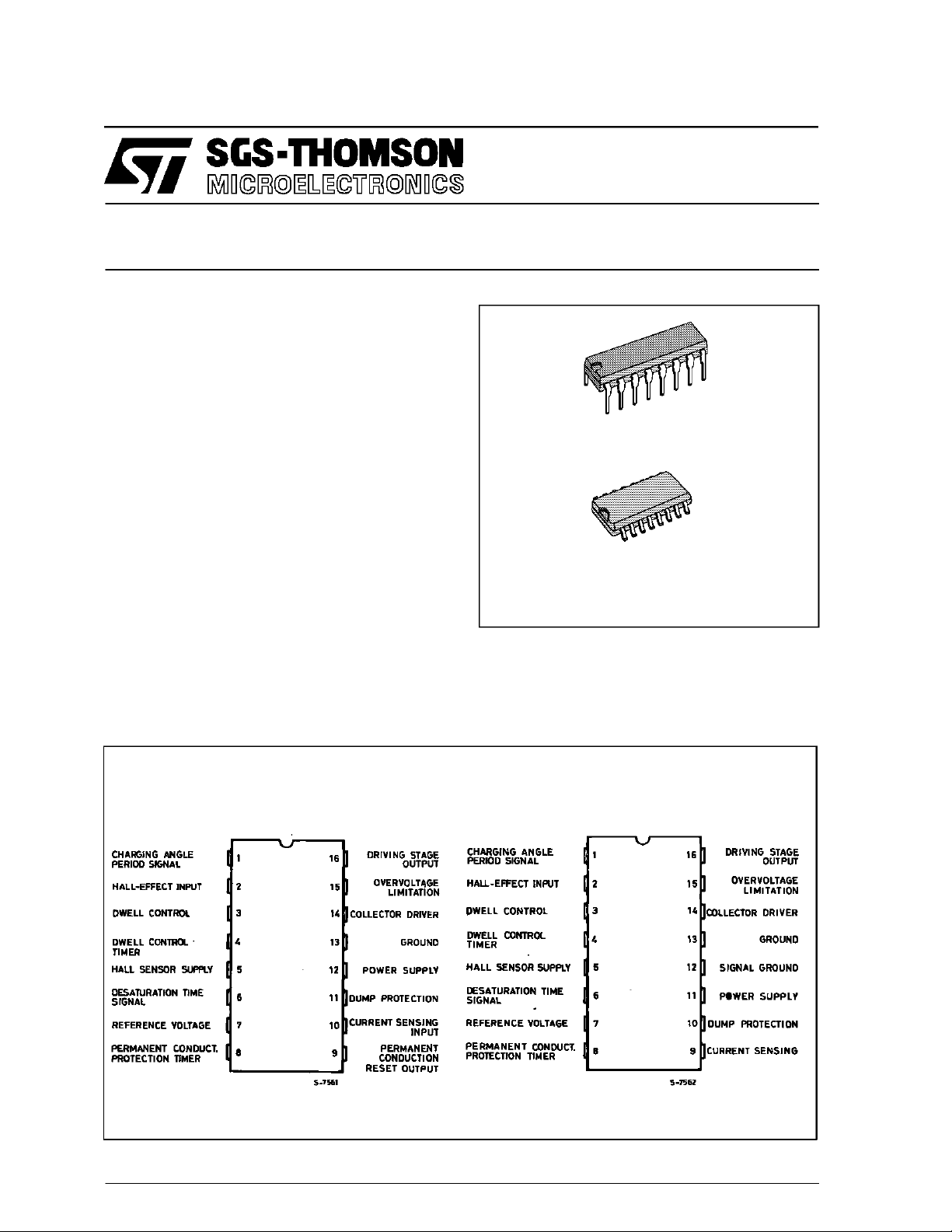
PI N CONNECTI ONS (top views)
DIP16
SO16
ORDERING NUMBERS : L482 (DIP16)
L482D1(SO16)
The L482isalsoparticularlysuitableforuseasignition controland driving stage in more sophisticated
car electronicsystems which employmicroprocessor cir cuits.
SO16
November 1991
1/11

L482
ABSOLUTEMAXIMUM RATINGS
Symbol Parameter Value Unit
V
R
V
D
P
tot
T
j,Tstg
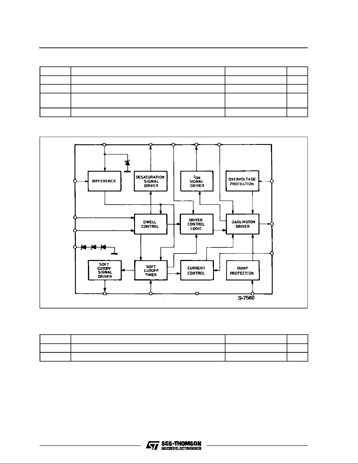
BLOCK DIAGRAM
Reverse Battery Voltage – 14 V
Dump Voltage 100 V
Power Dissipation at T
=90°C SO16
amb
DIP
1.2
0.65
Junction and Storage Temperature Range – 55 to 150 °C
W
W
THERMALDATA
Symbol Parameter Value Unit
R
th j-amb
R
th j-al
(*)Thermalresistance junction-aluminia with thedevice soldered onthe middle of an aluminiasupporting substrate measuring 15 x 20mm;
0.65mm thickness with infiniteheatsink.
2/11
Thermal Resistance Junction-ambient (DIP16) Max 90 °C/W
Thermal Resistance Junction-alumina (SO16) Max 50 °C/W

PINFUNCTIONS (refer to fig. 3 for DIP16 package)
N° Name Function
1 CONDUCTION TIME
SIGNAL
2 HALL-EFFECT INPUT Hall-effect Pickup Input. A high level on this pin enables the current driving
3 DWELL CONTROL The average voltage on the capacitor C
4 DWELL CONTROL TIMER The capacitor C5 connected between this pin and ground is charged when
5 HALL SENSOR SUPPLY This pin can be used to project the Hall-effect pickup against the voltage
6 DESATURATION TIME
SIGNAL
7 REFERENCE VOLTAGE A resistor R11 connected between this pin and ground sets the internal
8 PERMANENT CONDUCT.
PROTECTION TIMER
9 PERMANENT CONDUCT.
RESET OUTPUT
(no available in
Micropackage) (*)
10 CURRENT SENSING
INPUT (*)
11 DUMP PROTECTION
(*)
A low level on this output signal indicates when the external darlington is in
the ON condition i.e. when the current flows through the coil (ton in fig.1)
into the coil. The effective coil charge will be a function of the dwell control
logic. A High to Low transition from the Hall-effect pickup is the signal for
ignition actuation. The input signal, supplied by the open collector output
stage of the Hall-effect sensor, has a duty cycle typically about 70%.
connected between this pin and
2
ground depends on the motor speed and the voltage supply. The
comparison between V
and VC5voltages determines the timing for the
C2
dwell control. The recommended value is 100nF using a 100KΩ resistor at
pin 7. For the optimized operation of the device, C2 = C5.
the Hall-effect output is high and is discharged at the High to Low transition
of the Hall-effect signal. The recommended value is 100nF using a 100KΩ
resistor at pin 7.
transients, The resistor R
limits the current into the internal zener.
a
Open Collector Output Signal. This output is high when the external
darlington is in desaturation condition (current limitation), see t
d
1.
current used to drive the external capacitors of the dwell control (C
) and permanent conduction protection (C1). The recommended value is
C
5
100KΩ.
A capacitor C1 connected between this pin and ground determines the
intervention delay of the permanent conduction protection, t
With a 1µF capacitor and 100KΩ resistorR
at pin 7 the typical delay is 1s.
11
of the figure 2.
pc
A low pulse on this output detects the intervention of the permanent
conduction protection, as shown in figure 2. Typically the duration of the
time t
is more than 100µs.
r
Connection for Coil Current Limitation. The current is measured on the
sense resistor R
and divided on R1/R2. The current limitation value is
S
given by :
I
SENS
= V
SENS
R1 + R2
⋅ R2
R
S
The device is protected against the load dump. In load dump condition an
internal circuit, based on a zener diode and a darlington transistor,
switches off the external darlington and short circuits the supply.
By means of the external divider R8/R9 the protection threshold can be
changed and is given as first approximation by:
L482
pulse in fig.
and
2
R8+ R
= 8.5 ⋅
V
Dth
9
R
9
+ 5 ⋅ 10
−4
⋅ R
8
(the resistor R9 value must be higher than 4KΩ).
12 POWER SUPPLY (*) Supply Voltage Input. A 7V (typ) zener is present at the input. The external
resistor R
limits the current through the Zener for high supply voltages.
7
3/11

L482
PINFUNCTIONS (continued)
N° Name Function
13 GROUND This pin must be connected to ground.
14 DRIVER COLLECTOR The collector current for the internal driver which drives the external
15 OVERVOLTAGE
LIMITATION
darlington is supplied through this pin. The external resistor R
dissipation in the IC. The value of the resistor depends is a function of the
darlington used and on the limiting current in the coil.
The external is protected against overvoltage by means of an internal
zener available at this pin. The external divider R
defines the limitation
5/R6
value, given as first approximation by:
30
=
R
5
+ 5 ⋅ 10
V
ovp
−3
⋅ R6+ 30
10
limits the
16 DRIVING STAGE
OUTPUT
Current Driver for the External Darlington. To ensure stability and precision
of Tdesat C
and R3must be used. Recommended value for R3 is 2KΩ in
3
order not to change the open loop gain of the system.
may be added to C3to obtain greater flexibility in various application
R
C
situations.
and RC values ranges are 1 to 100nF and 5 to 30KΩ depending on the
C
3
external darlington type.
(*)These pins referonly tothe DIP package type.
For the SO16 version the permanent conduction reset output signal is not availableand the pin 9 becomes the current sensing input. Pin 10
replacesthe pin 11 function, pin 11 becomes thepower supply inputand pin 12 is usedas thesignal ground.
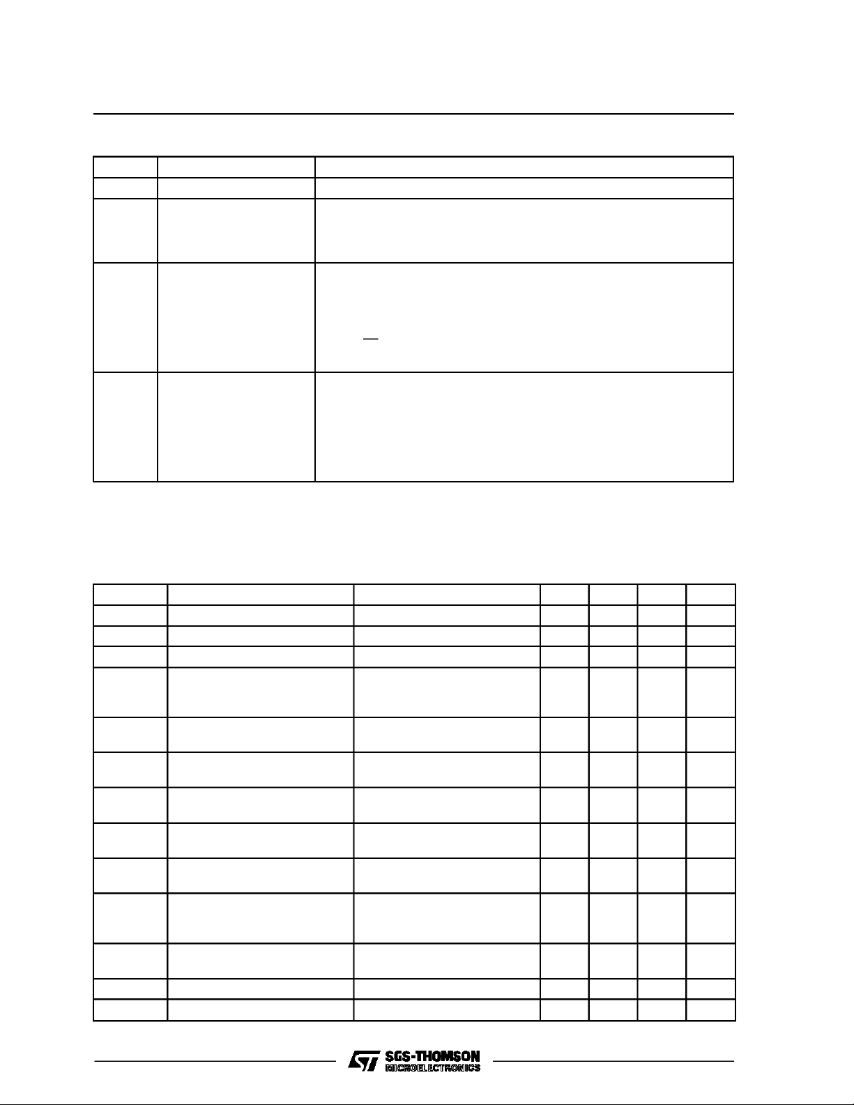
ELECTRICAL CHARACTERISTICS (VS=14V, –40°C≤Tj≤125°C referred to application circuit of
figure 3 regarding DIP-16 package version)
Symbol Parameter Test Conditions Min. Typ. Max. Unit
V
S
I
S
V
Z
V
I
I
I
V
Hz
I
HZ
V
CE sat
(V14–V16)
V
SENS
I
3D
I
3C
I3C/I
3D
V
OVZ
V
7
t
d
Operating Supply Voltage 6 28 V
Supply Current V12= 4.5V 25 mA
Zener Voltage (pin 12) IZ= 80mA 6.5 8.8 V
Sensor Input (pin 2)
LOW Voltage
HIGH 2.5
Sensor Input Current (pin 2) VI= LOW
= 6 to 16V
V
S
Hall-cell Supply Zener Voltage
IHz= 10mA 19 22 25 V
–12 –1 mA
0.5 V
V
(pin5)
Hall-cell Supply Zener Current
(pin5)
Series Darlington Driver Sat.
Voltage
Current Limit. Sensing Voltage
t = 10ms
=25°C
T
AMB
I
= 70mA
o
= 150mA 0.4
I
o
VS= 6 to 16V 200 400 mV
100 mA
0.6
1.0
V
V
(pin10)
C2 Discharge Current
C2 Charge Current
External Darlington Overvoltage
Protection Zener Voltage
VS= 6 to 16V
(*) Note 1
I
= 5mA to 15mA
OVZ
=25°C
T
AMB
0.2
5
6
3.4
20
35
25 30 35 V
µA
µA
Reference Voltage 2.5 3.5 V
Desaturation Time f = 40Hz VS= 14V 0.6 1.2 1.57 ms
4/11
 Loading...