

HIGHLY INTEGRATEDSLIC KIT TARGETED TO PABX
AND KEY SYSTEM APPLICATIONS
HIGHLY INTEGRATED SUBSCRIBER LINE
INTERFACE KIT FOR PABX AND KEY SYSTEM APPLICATIONS
IMPLEMENTS ALL KEY ELEMENTS OF THE
BORSCHTFUNCTION
INTEGRATEDZERO CROSSING BALANCED
RINGING INJECTION ELIMINATES EXTERNAL RELAY AND CENTRALISED RINGING
GENERATOR
ZERO NOISE INJECTED ON ADJACENT
LINES DURING RINGING SEQUENCE
LOW POWER IN STANDBY AND ACTIVE
MODES
BATTERY FEED WITH PROGRAMMABLE
LIMITINGCURRENT
PARALLELLATCHED DIGITAL INTERFACE
SIGNALLING FUNCTIONS (OFF HOOK,
GND-KEY)
LOW NUMBER OF EXTERNAL COMPO-
NENTS
INTEGRATEDTHERMAL PROTECTION
INTEGRATED OVER CURRENT PROTEC-
TION
0°CTO70°C: L3234/L3235
-40°CTO85°C: L3234T/L3235T
L3234
L3235
HEPTAWATT
ORDERING NUMBER: L3234
PLCC28
ORDERING NUMBER: L3235
injectorfabricatedin Bipolarin 140V Technology.
Its function is to amplify and inject in balanced
mode with zero crossing the ringing signal. The
DESCRIPTION
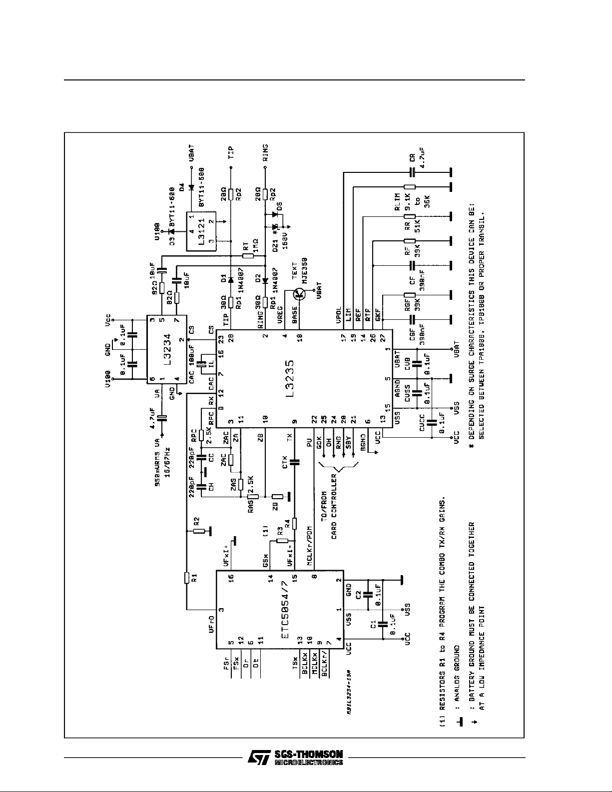
The L3234/L3235is a highly integrated SLIC KIT
targeted to PABX and key systemapplications
The kit integrates the majority of functions required to interface a telephone line. The
L3234/L3235implementsthe main featuresof the
broths function:
- Battery Feed (BalancedMode)
- Ringing Injection
- Signalling Detection
- Hybrid Function
The Kit comprises 2 devices, the L3234 ringing
Janauary 1995
This isadvanced information on a new product now in development or undergoing evaluation.Details are subject to change without notice.
device requires an external positive supply of
100V and a low level sinusoid of approx.
950mVrms. The L3235 Line Feeder is integrated
in 60V Bipolar Technology. The L3235 provides
batteryfeed tothe line with programmablecurrent
limitation. The two to four wire voice frequency
signal conversion is implemented by the L3235
and line terminating and balance impedancesare
externally programmable. The L3234/L3235kit is
designed for low power dissipation. In a short
loop conditionthe extrapower is dissipated on an
external transistor. The Kit is controlled by five
wire parallel bus and interfaces easily to all first
and programmable second generation COMBOS.
(seefigg. 1 and 2)
1/26

L3234 - L3235
Figure1: Typical ApplicationCircuit with SecondGeneration COMBO for Complete Subscriber Circuit
(Protection-SLIC-COMBO)
2/26
L3234 - L3235
Figure2: Typical ApplicationCircuit with First GenerationCOMBO for Complete Subscriber Circuit
(Protection-SLIC-COMBO)
3/26

L3234 - L3235
L3234
Solid State Ringing Injector
DESCRIPTION
The L3234 is a monolithic integratedcircuit which
is part of a kit of solid state devices for the subscriber line interface. The L3234 sends a ringing
signal into a two wires analog telephone line in
balanced mode. The AC ringing signal amplitude
is up to 60Vrms, and for that purpose a positive
supply voltage of +100V shall be available on the
subscribercard.
The L3234 receives a low amplitude ringing signal (950mVrms) and provide the voltage/current
amplification (60Vrms/70mA) when the enable input is active (CS > 2V). In disable mode (CS <
0.8V) the power consumption of the chip is very
low (<14mW).
The circuit is designed with a highvoltage bipolar
technology(V
>140V / V
CEO
CBO
>250V).
HEPTAWATT
The packageis a moulded plastic power package
(Heptawatt)suitable also for surface mounting.
BLOCK DIAGRAM
4/26
PIN CONNECTION (Top view)
L3234 - L3235
7
6
5
4
3
2
1
D94TL131
OUT2
V100
OUT1
GND
VCC
CS
VA
ABSOLUTE MAXIMUM RATINGS
Symbol Parameter Value Unit
V100 Positive Power SupplyVoltage +120 V
V
V
CS Logical Ring DriveInput V
T
T
5V Power Supply Voltage 5.5 V
CC
Low Voltage Ringing Signal (with V100 = 120Vdc) 1.4 Vrms
A
CC
Max. Junction Temperature 150
j
Storage Temperature -55 to +150
stg
OPERATINGRANGE
Symbol Parameter Value Unit
V100 High Power Supply Voltage 95 to 105 V
V
V
T
T
Low Power Supply Voltage 5 ±5% V
CC
Low Voltage Ringing Signal
A
Operating Temperature for L3234
op
Max. Junction Operating Temperature (due to thermal protection) 130 °C
jop
L3234T
600 to 950
within 10Hz -100Hz
0to70
-40 to 85
o
C
o
C
Vrms
°C
°C
Note: Operating ranges definethose limits between which the functionality ofthe device is guaranteed.
THERMAL DATA
Symbol Description Value Unit
R
th j-case
R
th j-amb
Thermal ResistanceJunction-case
Thermal ResistanceJunction-ambient
Max.
Max.
4
50
PIN DESCRIPTION
Pin Name Description
1 VA Low Voltage Ringing Signal Input
2 CS Logical Ring Drive Input
3V
CC
4 GND Common Analog-Digital Ground
5 OUT1 Ringing Signal Output
6 V100 +100V High Power Supply
+5V Low Power Supply
o
C/W
o
C/W
5/26

L3234 - L3235
OPERATIONDESCRIPTION
The Fig. 3 show the simplifiedcircuit configuration
Figure3: L3234/L3235Circuit Configuration
CO1
CO2
RO1
RO2
TIP
LINE TERMINALS
RING
LINE FEEDER
A
B
L3235
of the L3234 Solid State Ringing injector when
used with the L3235 Line Feeder.
+5VGND+100V
C100 CVCC
VCCGNDV100
643
CS
5
RINGING INJECTOR
7
L3234
2
CA
1
VA
VA
D94TL132
OUT1
OUT2
CS
GND
-VBAT
EXTERNALCOMPONENTSLIST
In the followingtable are shown the recommendedexternalcomponentsvalues for L3234.
Ref. Value Involved Parameter or Function
R01, R02 82Ω Ringing Feeding SeriesResistors
C01, C02 10µF - 160V Ringing Feeding Decoupling Capacitors
CA 4.7µF - 10V Low LevelRinging Signal De coupling Capacitor
C100 100nF - 100V Positive Battery Filter
CV
CC
When the ringing function is selected by the subscriber card, a low level signal is continuously applied to pin 1 througha de couplingcapacitor.Then
thelogicalringdrivesignalCS providedby L3235is
appliedto pin2 witha cadencedmode.
The ringing cycles are synchronised by the L3234
in such a way that the ringing starts and stops alwayswhenthe analoginputsignalcrosses zero.
When the ringing injection is enabled (CS = ”1”),
an AC ringing signal is injected in a balanced
6/26
100nF +5V Supply Filter
modeinto thetelephone line.
When the ringing injection is disabled (CS = ”0”),
the output voltage on OUT2 raises to the high
power supply, whereas on OUT1, it falls down to
ground.
The L3234 has a low output impedance when
sending the signal, and high output impedance
when the ringing signal is disabled
In fig. 4 the dynamic features of L3234 are
shown.
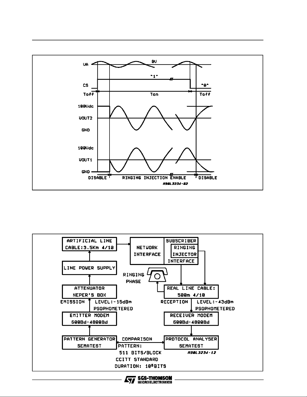
Figure4: Dynamic Features of L3234
L3234 - L3235
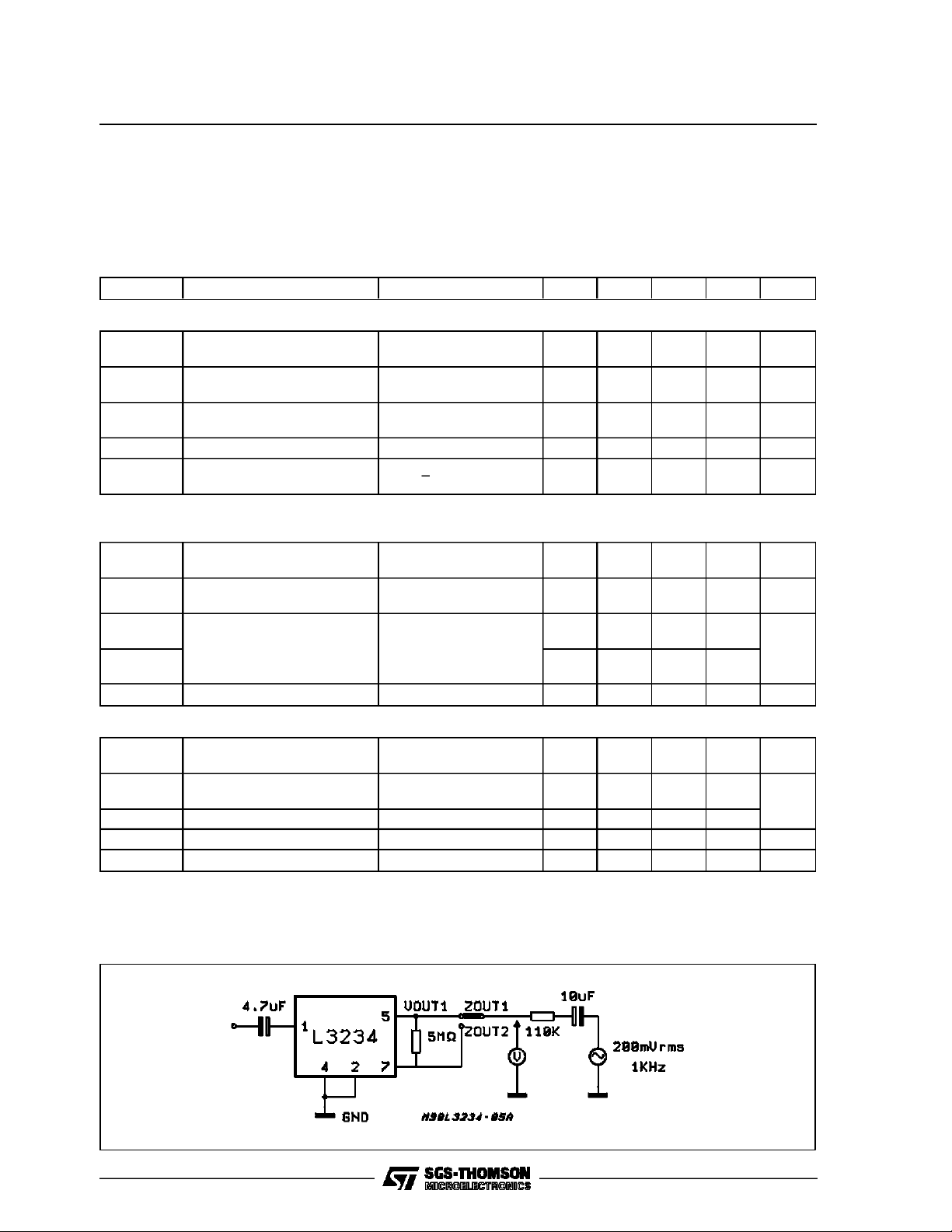
DATATRANSMISSION INTERFERENCE TEST
The L3234 meet the requirementsof the technical
specification ST/PAA/TPA/STP/1063 from the
CNET. The test circuit used is indicated below.
The measured error rate for data transmission is
lower than 10
This test measuresif during the ringing phase the
circuitinduce any noise to the closer lines.
Figure5: Test CircuitData TransmissionInterferenceTest
-6
during the ringing phase.
7/26
L3234 - L3235
ELECTRICAL CHARACTERISTICS (Test conditions:V100 = +100V,VCC= +5V, T
=25°C, unless oth-
amb
erwise specified)
Note: Testing of all parameteris performed at 25°C. Characterisation,as well as the design rule used al-
low correlation of tested performance with actual performances at other temperatures. All parameters listed here are met in the range 0°C to +70°C. For applications requiring operations in
the standard temperature range (0°Cto70°C) use L3234. If operations are required in the ex-
tended temperaturerange (-40°Cto85°C), use theL3234T.
Symbol Parameter Test Condition Min. Typ. Max. Unit Fig
STANDBY MODE: CS = ”0”
IS(V100)
I
S(VCC
V
SOUT1
V
SOUT2
Z
SOUT1
Z
SOUT2
THD Harmonic Distortion During
Consumption VA = 950mVrms; 50Hz 45
)
DC Output Voltage VA = 950mVrms; 50Hz
Output Impedance 70
Z
Matching 15 %
OUT
< 6dBm; f = 1kHz -46 -40 dB 7
V
LINE
Emission
92
70
560
100
800
µA
µA
6V
V
kΩ
kΩ
6
RINGINGPHASE: CS = ”1”
DC OPERATION
IR(V100)
I
)
R(VCC
V
ROUT1
V
ROUT2
V
IH
IIH(CS = 0)
V
IL
IIL(CS = 0)
I
lim
Consumption Z
DC Output Voltage VA = 0V 44
Threshold Voltage on the
Logical Input CS
DC Line Current Limitation VA = 0V 70 150 mA 12
= ∞
LINE
VA = 950mVrms; 50Hz
44
VA = 950mVrms; 50Hz 2.0
2.5
2.2
5
3
56
56
1
0.8
1
mA
mA
V
V
V
µA
V
µA
8
AC OPERATION
V
/VA
OUT1
V
/VA
OUT2
V
OUT1-VOUT1
Ringing Gain Z
Ringing Signal ZLINE = 2.2µF+1kΩ
= 2.2µF+1kΩ
LINE
VA = 0dBm
29.5
29.5
30
30
57 60 Vrms
VA = 950mVrms; 50Hz
THDV
(VA) InputImpedance VA = 950mVrms; 50Hz 40 kΩ 10
Z
IN
Z
OUT
Harmonic Distortion VA = 950mVrms; 50Hz 5 %
LINE
Differential Output Impedance I
< 50mArms 20 Ω 11
LINE
TEST CIRCUITS
Figure6.
8/26
dB
dB
9
9
 Loading...