

SGS Thomson Microelectronics L3121B Datasheet
L3121B
ApplicationSpecific Discretes
A.S.D.
FEATURES
BIDIRECTIONALFUNCTIONWITH VOLTAGE
PROGRAMMABILITYIN BOTH POSITIVEAND
NEGATIVEPOLARITIES.
PROGRAMMABLE BREAKDOWN VOLTAGE
UP TO100 V.
HOLDINGCURRENT = 150mA min.
HIGHSURGE CURRENTCAPABILITY.
IPP= 100A, 10/1000µs
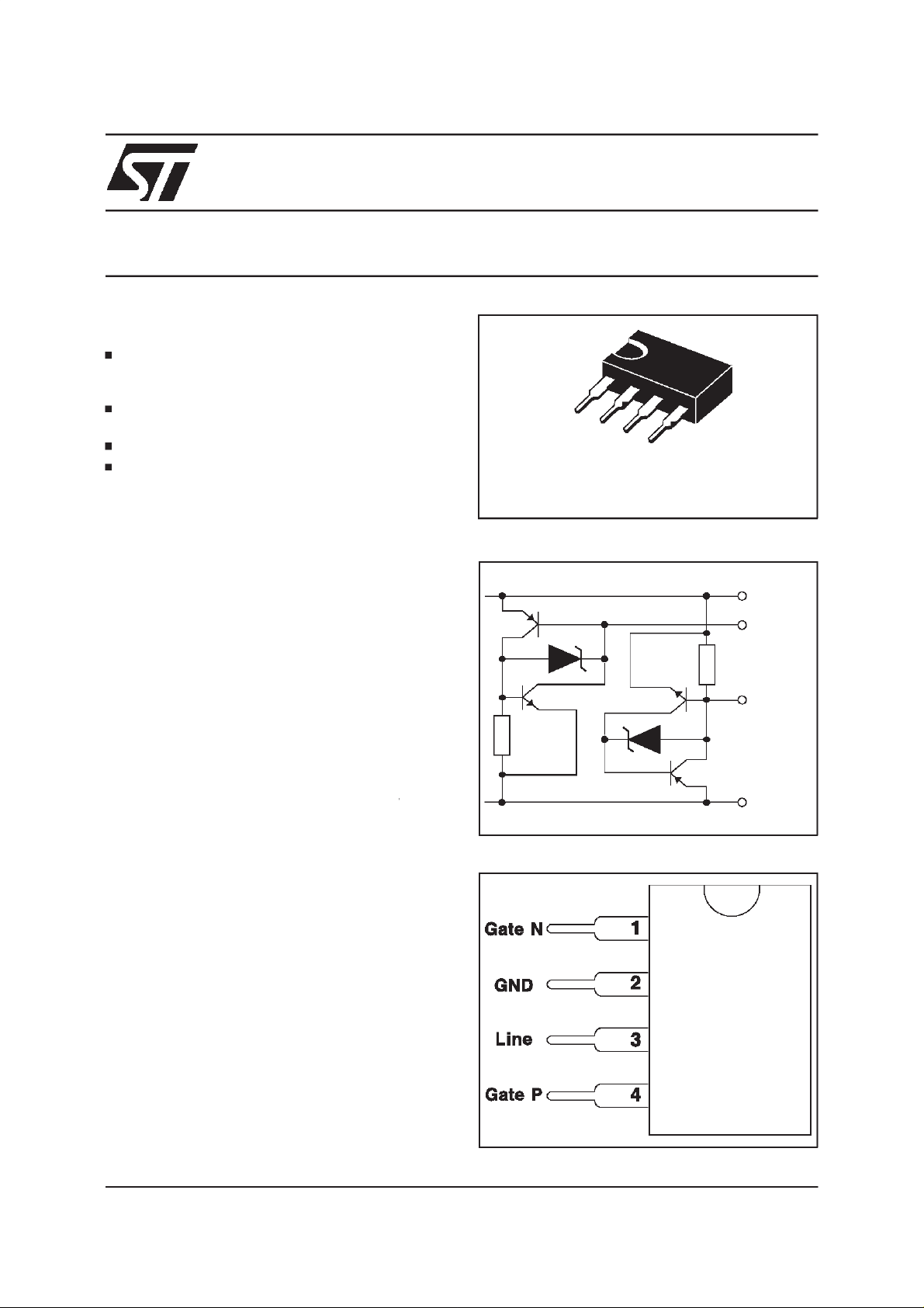
DESCRIPTION
This device has been especially designed to protect a subscriber line interface circuit (SLIC) with
anintegratedring generator.
Used with the recommended application circuit,
eachline(TIPand RING)is protectedagainstpositive and negative surges. In the positive polarity,
the breakdownvoltage is referenced to the + VB ,
andinthe negativepolarity,the breakdownvoltage
isreferencedto the -Vbat .
TM
PROGRAMMABLE TRANSIENT VOLTAGE
SUPPRESSORFOR SLIC PROTECTION
SIP4
SCHEMATIC DIAGRAM
Line
Gate P
Gate N
Itshigh surgecurrentcapabilitymakesthe L3121B
areliableprotectiondevicefor veryexposedequipment,or when series resistorsare very low.
May 1999 - Ed:4A
GND
CONNECTION DIAGRAM
1/7
L3121B
COMPLIESWITHTHE
Peak Surge
FOLLOWING STANDARDS:
ITU-T K20
VDE0433
VDE0878
IEC1000-4-5
FCC Part 68, lightning surge
type A
FCC Part 68, lightning surge
type B
BELLCORE TR-NWT-001089
First level
BELLCORE TR-NWT-001089
Second level
ABSOLUTE MAXIMUM RATINGS
Voltage
(V)
4000 10/700 5/310 100 4000 10/700 5/310 100 4000 1.2/50 1/20 100 -
level4
level4
1500
800
1000 9/720 5/320 25 2500
1000
5000 2/10 2/10 250 10
(Tamb= 25°C)
Voltage
Waveform
(µs)
10/700
1.2/50
10/160
10/560
2/10
10/1000
Current
Waveform
(µs)
5/310
8/20
10/160
10/560
2/10
10/1000
Admissible
Ipp
(A)
100
100
200
100
250
100
Necessary
Resistor
(Ω)
Symbol Parameter Value Unit
I
PP
I
TSM
V
MLG
V
MGL
T
stg
T
j
T
L
Top
Note 1: Variation ofelectrical parameters is given by curves.
Peak pulse current
Non repetitive surge peak on-state
current
Maximum voltage LINE/GND.
Maximum voltage GATE/LINE.
Storage temperature range
Maximum operating junction temperature
Maximum lead temperature for soldering during 10s
Operating temperature range (see note 1)
10/1000µs
2/10µs
100
250
tp = 10 ms 50 A
100
80
- 40 to +150
+ 150
260 °C
-40to+85 °C
-
-
-
-
-
-
A
V
V
°
C
°C
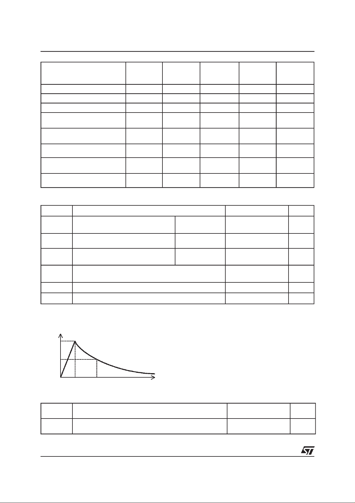
Pulsewaveform10/1000µs
%I
PP
100
50
0
t
r
t
p
THERMAL RESISTANCE
Symbol Parameter Value Unit
Junction-to-ambient
2/7
R
th (j-a)
t
80 °C/W

L3121B
ELECTRICALCHARACTERISTICS
Symbol Parameter
V
RM
I
RM
V
BR
V
BO
I
H
I
BO
I
PP
V
GN
I
GN,IGP
C
Stand-off voltage
Reverseleakagecurrent
Breakdown voltage
Breakover voltage
Holding current
Breakover current
Peak pulse current
Gate voltage
Triggeringgate current
Capacitance
1- OPERATIONWITHOUT GATE
I
RM
Type
max. min. max. typ. max. min. max.
(T
@V
amb
RM
=25°C)
VBR@I
R
I
IPP
I
BO
IH
V
BO
@I
BO
I
note1 note 1 note2
VRM
VBO
VBR
H
C
µA V V mA V mA mA mA pF
L3121B
5
8
60
90
2- OPERATIONWITH GATE
@IGN= 200mA IGN@VAC= 60V IGP@VAC= 60V
V
GN
Type
min. max. min. max. max.
V V mA mA mA
L3121B
Note 1 :
See the reference testcircuits for IH,IBOand VBOparameters.
Note 2 :VR= 5 V, F = 1MHz.
0.6 1.8 80 200 180
100 1 180 200 500 150 200
3/7
 Loading...