

SUBSCRIBER LINE INTERFACE CIRCUIT
MONOCHIP SILICON SLIC SUITABLE FOR
PUBLIC/PRIVATEAPPLICATIONS
IMPLEMENTS ALL KEY FEATURES OF THE
BORSCHTFUNCTION
SOFT BATTERY REVERSAL WITH PROGRAMMABLETRANSITION TIME(3 to 100ms)
METERING PULSE INJECTION AND FILTERING WITH MINIMAL COMPONENTS COUNT
(NO TRIMMING REQUIRED).
PROTECTION RESISTOR MISMATCH COMPENSATION
ON HOOKTRANSMISSION
LOOP START/GROUNDSTARTFEATURE
IND TEMP. RANGE:
-40°C TO +85°C
LOW POWER DISSIPATION IN ALL OPER-
ATING MODES
INTEGRATED ZERO CROSSING RELAY
DRIVER
INTEGRATED (NOISE-LESS) RING TRIP DE-
TECTION
VERY LOW NO. of STD TOLERANCE EX-
TERNAL COMPONENTS
SELECT PART FOR U.S. APPLICATIONS
(63dB TYP. LONG.BALANCE)
SURFACE MOUNT PACKAGE (PLCC44 or
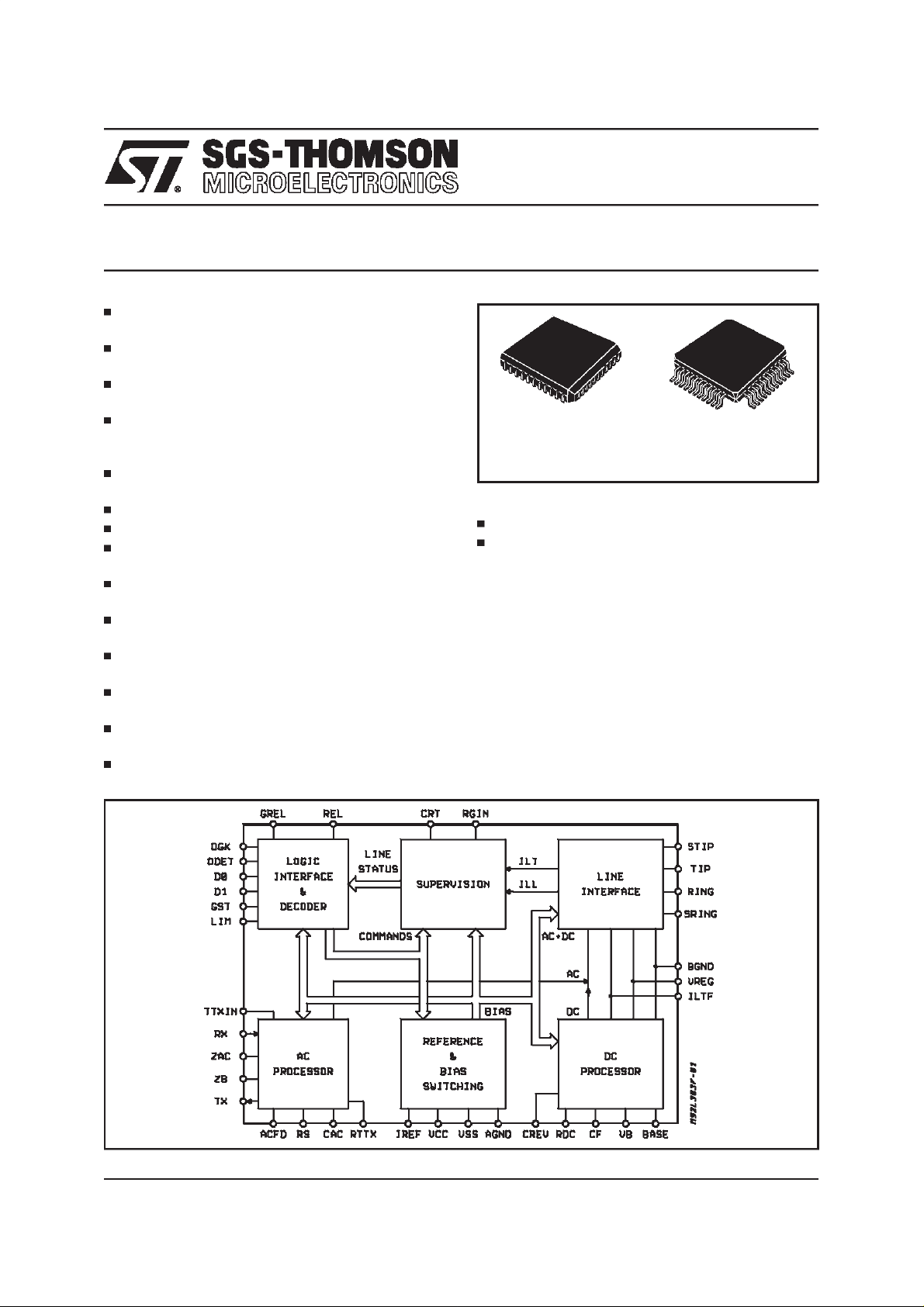
BLOCK DIAGRAM
L3037
PLCC44 PQFP44(10 x 10)
ORDERING NUMBERS:
L3037FN L3037QN
PQFP44)
INTEGRATEDTHERMAL PROTECTION
PIN TO PIN COMPATIBLEWITH L3035/36
DESCRIPTION
The L3037 subscriber line interfacecircuit is a bipolar device in 70V technologydeveloped for centraloffice/ loop carrierandprivateapplications.
The L3037 is pin to pin and function compatible
with L3035/36. One particular pin (reserved in
L3035/36) is now used for reverse polarity transition time programming.The line polarity transition
is not affecting the AC signal transmission that
can continue also during the line voltage transition.L3037 is available in two different package
options:PLCC44 and PQFP44 (10 x 10mm).
December 1997
This is advanced information on a new product now in development or undergoing evaluation. Details are subject to change without notice.
1/22

L3037
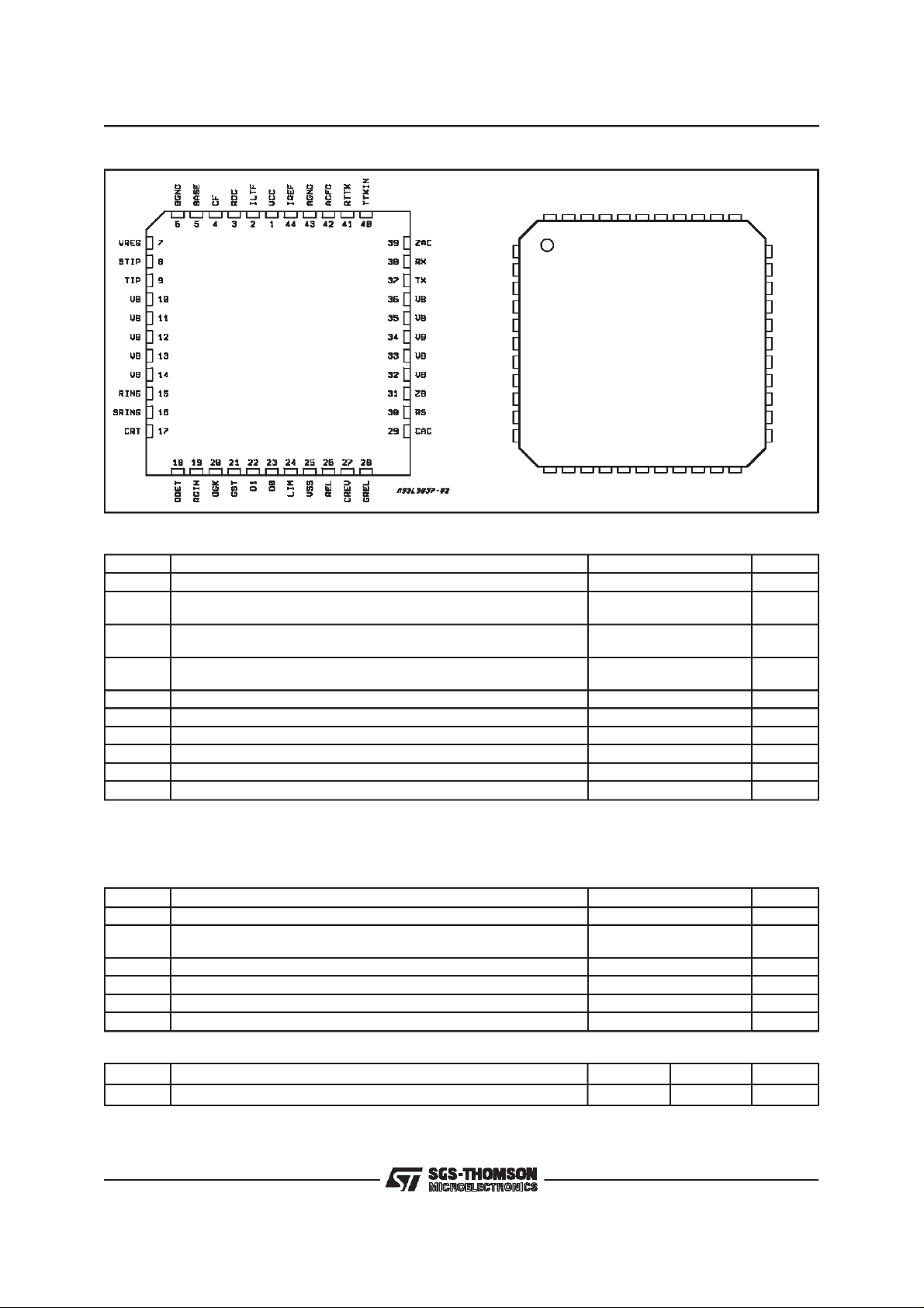
L3037 PIN FUNCTIONALITY(PLCC44)
No. Name Function
1
2
3
4
5
6
7
8
9
10 to14
15
16
17
18
19
20
21
22
23
24
25
26
27
28
29
30
31
32 to 36
37
38
39
40
41
42
43
44
V
CC
I
LTF
RDC
CF
BASE
BGND
VREG
STIP
TIP
VB
RING
SRING
CRT
ODET
RGIN
OGK
GST
D1
D0
LIM
V
SS
REL
CREV
GREL
CAC
RS
ZB
VB
Tx
Rx
Z
AC
TTXIN
RTTX
ACFD
AGND
I
REF
Supply input (+5V)
Analog output (current source)
Analog input (current input)
Analog input (voltage input)
Analog output (voltage source)
Ground input (0V)
Supply input (VREG)
Analog input (voltage input)
Analog output (voltage output)
Supply input (-V
BAT
)
Analog output (voltage output)
Analog input (voltage input)
Analog input/output (voltage input / current output)
Digital output (voltage output with internalpull up)
Analog input (current input)
Digital output (voltage output with internalpull up)
Digital input (voltage input, internal pull down)
Digital input (voltage input)
Digital input (voltage input)
Digital input (voltage input 3 levels: 0, +5, open)
Supply input (-5V)
Digital output (voltage output open drain)
Analog input/output (voltage input/current output)
Ground input (0V)
Analog input (current input)
Analog input/output (current output/voltage input)
Analog input (voltage input)
Supply input (-V
BAT
)
Analog output (voltage output)
Analog input (voltage input)
Analog output (voltage output)
Analog input (voltage input)
Analog output (voltage output)
Analog input (voltage input)
Ground input (0V)
Analog input/output (voltage output/current input)
L3037 FUNCTIONAL DIAGRAM
OGK
ODET
D0
AC
LINE
STATUS
1
TTXIN
2/22
D1
GST
LIM
RX
ZAC
ZB
TX
D94TL136
LOGIC
INTERFACE
&
DECODER
1
-
+
1
2.32
PROCESSOR
ACFD RS CAC RTTX IREF VCC VSS AGND CREV VB CF BASE
CRTRELGREL RGIN
ICRT
ILT
ICRTVREF
SUPERVISION
COMMANDS
REFERENCE
SWITCHING
&
BIAS
0 CROSS
DETECT.
BIAS
ILT
ILL
AC+DC
(IA+IB)/200
(IA-IB)/200
LINE
INTERFACE
PROCESSOR
IREV
AC
DC
(IA+IB)/200
DC
1
-1
REGULATOR
IA
IB
SUPPLY
STIP
TIP
RING
SRING
BGND
VREG
ILTF
RDC
L3037
PIN CONNECTION
(Topview)
PLCC44
VREG
STIP
TIP
N.C.
N.C.
N.C.
RING
SRING
N.C.
CRT
CC
ILTF
IREF
AGND
N.C.
ACFD
REL
CREV
RTTX
GREL
33
32
31
30
29
28
27
26
25
24
23
D94TL129
BGND
BASECFRDC
44 43 42 41 3940 38 37 36 35 34
1
VB
2
3
4
5
6
7
8
9
10
12 13 14 15 16
ODET
RGIN
PQFP44
OGK
V
171118 19 20 21 22
D0
D1
GST
LIM
SS
V
ABSOLUTE MAXIMUM RATINGS
Symbol Parameter Value Unit
V
V
V
V
agnd
V
V
V
I
T
bgnd
REL
dig
T
Battery Voltage -64 to VSS+0.5 V
bat
Positive Supply Voltage (0 to 1ms)
CC
(continuous)
Negative Supply Voltage (0 to 1ms)
SS
(continuous)
-
Agnd Respect Bgnd (continuous) -2 to +2 V
-0.4 to +7
-0.4 to +5.5
-7 to +0.4
-5.5 to +0.4
Ring Relay Supply Voltage 14 V
Digital I/O D0, D1, GST, LIM, ODET, OGK -0.4 to +5.5 V
dig
Digital I/O D0, D1, GST, LIM, ODET, OGK -3 to +3 mA
Maximum Junction Temperature +150 °C
j
Storage Temperature -55 to +150 °C
stg
Hu Humidity 5 to 95 %
Note: In caseof poweron, power failureor hotinsertion withVDD,VSSpresent andV
with Vbat> V
not controlled. This effect can be prevented ensuring that Vbat is always present before V
(e.g. BAT49X or equivalent) between Vbat and V
+0.5V. In this case the power consumption of the device increases and the logic output state including relay driver are
SS
. One diode can be shared between all the SLICs of the same line card.
SS
floatingthe AbsoluteMaximum Ratings can be exceeded
bat
and VSSor connecting one shottky diode
DD
OPERATINGRANGE
TTXIN
ZAC
RX
TX
N.C.
VB
N.C.
N.C.
ZB
RS
CAC
V
V
V
V
Symbol Parameter Value Unit
V
T
agnd
V
V
V
V
V
bgnd
REL
Operating Temperature Range -40 to +85 °C
op
-
Difference between Agnd and Bgnd -2 to +2 V
Positive Supply voltage +4.5 to +5.5 V
CC
Negative Supply Voltage -5.5 to -4.5 V
SS
Battery Voltage -62 to -17 V
bat
Ring Relay Supply Voltage 4 to 13 V
THERMAL DATA
Symbol Parameter PLCC44 PQFP44 Unit
R
th j-amb
Thermal Resistance Junction-ambient Max. 45 75
C/W
°
3/22

L3037
PIN DESCRIPTION
Unless otherwise specified all thediagrams in this datasheet refers to the PLCC44 Pin Connection.
PQFP44
No.
39 1 V
40 2 I
41 3 RDC DC feedback input (the RDC resistor is connected from this node to I
42 4 CF Battery voltage ripple rejection (C
PLCC44
No.
Pin Description
Positive Power Supply (+5V)
CC
Transversal Line Current Image ((IA+IB) / 200)
LTF
capacitor is connectedfrom this node to BGND).
SVR
LTF
)
43 5 BASE Driver for external transistor base
44 6 BGND Battery ground
2 7 VREG Regulated Voltage. Provides negative power supply for the power amplifier.
(connected to emitter of theexternal transistor.)
3 8 STIP Input of A power amplifier (when no compensation of ext. ptc resistor mismatchis
requested it must be shorted to the TIP lead).
4 9 TIP A line termination output (I
1, 28 10 to 14
32 to 36
VB Battery Supply
PLCC44: All pins are internally connected together.
is thecurrent sourcedfrom this pin).
A
PQFP44: It is mandatory to short pin 1 and pin 28 as closed as possible to thedevice.
8 15 RING B line termination output (I
is thecurrent sunkinto this pin).
B
9 16 SRING Input of B power amplifier (when no compensation of ext. ptc resistor mismatchis
requested it must be shorted to the RING lead).
11 17 CRT Ring trip and ground key capacitor
12 18 ODET ON/OFF hook and RING TRIP output (when disable is internally pulled up)
13 19 RGIN Ring input signal. (when openis internally pulled to GND)
14 20 OGK Ground key output (when disable is internally pulled up)
15 21 GST A open command (whenopen is internally pulled down)
16 22 D1 Bit 1
17 23 D0 Bit 0
18 24 LIM Current Limitation Program. (when open is internally forced to 44mA current limitation)
19 25 V
Negative Power Supply (-5V)
SS
20 26 REL Ring relay driver output
21 27 CREV Reverse polarity transition time control. One proper capacitor connected between this
pin and AGND is setting the reverse polarity transition time. If reverse polarity feature
is not used must be open or connected to AGND through a filter capacitor.
22 28 GREL Ground reference for ring relay driver
23 29 C
24 30 R
25 31 Z
AC feedback input (ACDC split capacitor is connected from this node to ILTF)
AC
Protection resistors image(the image resistor is connected from this node to ACFD)
S
Balance network for 2 to 4 wire conversion (the balance impedance ZBisconnecetd
B
from this node to AGND. The Z
impedance is connected from this node to ZAC)
A
30 37 Tx 4 wire outputport (Tx output)
31 38 Rx 4 wire receiving port. (Rx input)
32 39 Z
33 40 TTXIN Metering input port/V
Rx buffer output (the AC impedance is connected from thisnode to ACFD)
AC
programming. If notused should be connected to AGND.
drop
34 41 RTTX Metering cancellationnetwork. If not used should be left open.
35 42 ACFD AC impedance synthesis
37 43 AGND DC andAC signalground
38 44 I
2,5 to 7,
10,26,
–
N.C. Not connected
Voltage Reference Output
REF
27, 29,36
4/22

L3037
DESCRIPTION
(continued)
One special selection with high longitudinal balance performancesallows to meet the UnitedStates
BELLCORE requirements for central office/loop
carrier and privateapplications.
The SLIC integrates loop start, ground start,
ground key on/off-hook,automatic ring-trip as well
as zero crossing ring relaydriver.
Two to four wire conversionis implemented by the
SLIC for application with first generation COMBO.
In caseof applicationwith secondgeneration (programmable) COMBO this function can be implementedoutsidesavingexternalcomponents.
The L3037 offers programmablecurrent limitation
(3 ranges), on hook transmission and low power
in all operating modes, power management is
controlled by a simpleexternallow costtransistor.
Metering pulses are injectedon the line via a summingnodethroughTTXIN pin.
Metering pulse filtering is performed by means of a
simple RC networkwith standardtolerancecomponents. In case TTX function is not used this pin
must be connected to AGND. It is also possible to
usethis pin to modifythe DC voltagedropbetween
TIP/RING terminalsand batteryvoltagefor appications where it is important to optimize the battery
voltagesupplyversusthesignalswing.
Effect of protection resistors mismatch are compensated by a feedbackloop on thefinal stageallowing good long balance performances also with
large toleranceprotection resistors(ex: PTC).
This function allow the L3037 to be fully conform
to BELLCORE power cross and surge test and
meet also the Longitudinal Balance Specification
without using matched PTC resistors.
An integrated thermal protection circuit forces the
L3037 in POWER DOWN (PD) mode when the
junction temperature exceeds 150°C Typ.
The L3037 is specified over -40°C to +85°Cam-
bient temperaturerange.
The L3037 package is a surface mount PLCC44
or PQFP44.
FUNCTIONAL DESCRIPTION
L3037 is designed in 70V bipolar technology and
performs the telephone line interface functionsrequired in both C.O. and PABXenvironments. The
full range of signal transmission, battery feed,
loop supervisionare performed.
Signal transmission performance is compatible
with European and North American Standards
and with CCITT recommendations.
Ringing, overvoltage and power cross protection
are performed by meansof externalnetworks.
The signal transmission function includes both 2
to 4 wire and 4 to 2 wire conversion.The 2W termination impedance is set by means of an external impedancewhich may be complex. The 2 to 4
wire conversion is provided by meansof an external network.
Such a network can be avoided in case of applications with COMBOII, in this case the 2 to4 wire
conversion is implemented inside the COMBOII
by means of the programmableHybal filter.
An additionalinput allows a meteringpulse signal
to be added on the line.
The DC feed resistance is programmable with
one external resistor. Three different values of
current limitation (25, 44, 55mA)can be selected
by softwarethrough the parallel digital interface.
One external transistor reduces the power dissipation inside the L3037 in the presence of a short
loop (limiting current region).
An additional supervisory function sets the TIP
lead into high impedance state in order to allow
applicationin ground start configurations.
The different L3037 operating modes are controlled by a 4bit logic interface, two additional detector outputs provide ground key detection and either hook state or ring tripdetection.
SLIC OPERATINGMODES
Through the L3037 digital interface it is possible
to select 5 differentSLIC operatingmodes:
1) Active Mode (ACT)
2) StandbyMode (SBY)
3) Tip Open Mode (TO)
4) Power Down Mode (PD)
5) Ringing Mode (RNG)
In both ACT and SBY modes it is possible to se-
lect the reversepolarity (see control interface).
Transition from direct to reverse polarity is soft
and the transition time is defined by the external
capacitorCREV.
ACTIVEMODE(ACT)
This operating mode is set by the card controller
whenthe Off-Hookconditionhas beenrecognized.
When this operatingmode is selected the two out-
put buffers (TIP/RING) can sink or source up to
100mA each. In case of Ground key or line terminals to GND the outputcurrent is limited to 15mA
fortheTipwireand 30mA for the Ringwire.
As far asthe DC characteristicis concernedthree
differentfeeding conditionsare present:
a) Current limiting region: the DC impedance of
the SLIC is very high( 20Kohm) and therefore the
system works like a current source. Using the
L3037 digital interface it is possible to select the
value of the limiting current:
25mA, 44mA, or 55mA.
When the device is in limiting current region the
negative supply for the output buffer is fixed by
5/22

L3037
the ext. transistor to a proper value higher than
the real negative battery in order to reduce the
power dissipatedby the L3037 itself.
b) Resistive feed region: the characteristic is
equal to a battery voltage (Vbat) in series with a
resistor (typ 400ohm or 800ohm) whose value is
set by one ext.resistor(see ext. componentslist).
c) Constant voltage region: the characteristic is
equal to the battery voltage - 12V in series with
the ext. protectionresistors (typ 80ohm).
This voltage drop between battery and line terminals forIl=0 allowson-hooktransmission.
Fig. 1 shows the DC characteristic in active
mode. Fig. 2 shows the line current versus loop
resistance
Figure 1:
DC Characteristicin activemode
Figure 2: Currentvs. Loop Resistance.
Rfeed = 2 x 200ohm,
Lim. currents: 25, 43, 55mA
1) The lineimpedance (Zline)
2) The SLIC impedance at line terminals (Zs)
3) The balancingnetworkZA+RA connected
betweenpin ZAC and ZB of L3037.
4) The networkZB betweenpin ZB and GND
thatshall copy the line impedance.
When L3037 is used with a second generation
combo(eg TS5070FN)which is able to performthe
two to four wire conversion, the two impedances
ZA and ZB can be removed and the ZB pin connectedto GND.The -6dB TX gainof the L3037allows the echo signal to remain always within the
COMBOIIHybridbalancefilterdynamicrange.
The injection of high frequency metering pulses is
carried out throughthe SLIC. An unbalanced12 or
16KHzsinusoidal signal with shapingis, when necessary,appliedattheTTXINinputof the SLIC.
A fixedtransfer gain is providedforthe metering signal. To avoid saturation in the 4-wire side a cancellationis providedin the4-wiretransmissionpath.
Cancellation is obtained via an external RC networkwithout the needfor trimmed components.
When the TTX function is not used TTXIN input
should be connectedto GND. Since this pin is directly connected to a summing node inside the
SLIC any signal applied to the TTXIN is transferred to the line witha fixedtransfer gain.
In special applications, this pin can be used to
modify the voltage drop (constant voltage region
of DC characteristic) simply by applying a proper
DC level on the TTXIN pin, allowing optimization
of the battery voltage versus the maximum needed AC signalswing.
In active mode, with a -48V battery voltage, the
L3037 dissipate 150mW for its own operation (including the power dissipation from +5/-5 supply),
the dissipation related to the current supplied to
the line should be added in order to get the total
dissipation.
In active mode the AC impedance at the line terminals is sinthetized by the external components
ZAC and Rp according to the following formula:
Zs= ZAC/50+ 2*Rp
Depending on the characteristic of the ZAC network Zscan be either a pure resistance or a complex impedance.This allows L3037 to meet different standard as far as return loss is concerned.
The capacitor CCOMP guaranteesstability to the
system.
The two to four wire conversion is achieved by
means of a circuit that can be represented as a
Wheastone bridge, the branchesof which are:
6/22
STAND-BYMODE (SBY)
In this mode thebias current of the L3037 is redu-
cedand only somepartof the circuitarecompletely
active. The transversal current supplied to the line
islimited at 14mA.Common modecurrentrejection
is performed and the total current capability of the
output stages (TIP and RING) is limited to 30mA.
Theopencircuitvoltageis |Vbat|-7V.
Both Off/Hook and Ground key detectorsare active. Signal transmissionis not operating.
In stand-by mode, with a -48V batter y voltage, the
L3037dissipates90mWtyp.(includingthepowerdissipationfroma +5/-5Vsupply).
Stand-bymode isusuallyselectedwhen thetelepho ne is in on-hook conditi on.It allow sa properoff-hook
detection, even in the presence of high comm on
modecurrents,or with telephone sets sinking a few
milliamperesof line currentin on-hookconditi on.

CONTROLINTERFACE
L3037
INPUTS
D0 D1 GST LIM ODET OGK
POWER DOWN
0
1
1
1
1
0
0
0
(*) LIM = 0 → I
0
1
1
0
0
1
0
1
lim
0
0
1
0
1
0
1
1
= 25mA; LIM = H. I. (open) → I
X
X
X
X (*)
X (*)
X
X
X
STANDBY D. P.
STANDBY R. P.
ACTIVE D. P.
ACTIVE R. P.
RING
A. OPEN
RESERVED
lim
TIP OPEN MODE (TO)
This mode is selected when the SLIC is adopted
in a system using the Ground start feature. In this
mode the TIP terminationis set in High Impedance (100Kohm) while the RING termination is acti-
OPERATING MODE
= 44mA; LIM = 1 → I
DISABLE
OFF/HK
OFF/HK
OFF/HK
OFF/HK
RING-TRIP
OFF/HK
= 55mA.
lim
Once ring trip is detected the ringing signal is
automatically disconnected at the first zero crossing. When the ringing signal phase is not provided at the RGIN pin the ringing signal is disconnectedimmediately after ring trip detection.
OUTPUTS
–
ve and fixed at Vbat + 4.5V. In the case of connection of RING termination to GND the sinked
current is limitedto 30mA. When RING is connected to GND both off-hook and ground-key detectors becomeactive.
Power dissipation in thismode witha -48V battery
voltage is 100mW (including the power dissipation from +5/-5V supply).
POWERDOWN MODE (PD)
In thismode, both TIP and RING terminationsare
open and no current is fedinto the line.
The power dissipationis verylow.
This mode is usually selected in emergency con-
dition or when theconnected line is disabled.
This is also the mode into whichthe SLIC is auto-
matically forced, in the case of thermal overload
T
> 150°C typ.
j
RINGING MODE (RNG)
When this mode is selected the ringing signal is
injected on the line via the ext relay activated by
the L3037 relay driver.
When the ringing signal phase is provided at the
RGIN pin, the relay command is also synchronized with the ringing signal zero crossing.
The TIP and RING termination of the L3037 are
senses the line current which is then integrated
on theCRT capacitor.
TIP pin voltage is fixed at – 2.5V, RING pin voltage is fixed at V
+ 4.5V,TIP, RING buffer cur-
BAT
rent capability is limited to 100mA.
When off-hook occurs during ringing burst the
voltage on CRT increase above a proper thre-
EXTERNALCOMPONENTS LIST
To set the SLIC into operation the following para-
metershave to be defined:
- The DC feeding resistance ”Rfeed” defined as
the resistance of the traditional feeding
system (most common Rfeed values are:
400, 800, 1000 ohm).
- TheAC SLICimpedanceat lineterminals”Zs” to
whichthereturn lossmeasurementsisreferred.
Itcanbereal(typ.600ohm)or complex.
- The equivalent AC impedance of the line ”Zl”
used for evaluation of the trans-hybrid loss
performance (2/4wire conversion). It is usuallya compleximpedance.
- The value of the two protectionresistors Rp in
series with the line termination.
- The line impedanceat the TTXfreq. Zlttx.
- The reverse polarity transition time defined as
/∆T”.
”∆V
TR
Once, the above parameters are defined, it is
possible to calculate all the external components
using the followingtable.
The typical values has been obtainedsupposing:
- Rfeed = 400
Ω
- Zs = 600Ω
- Zl =600Ω
-Rp=40Ω
- Zlttx = 216Ω + 120nF @ 12KHz
- Re[Zlttx]= 216Ω
- Im[Zlttx]= -110Ω @12KHz
-∆V
/∆T = 4250[V/s]
TR
shold and ring trip is detected.
DISABLE
GDKEY
GDKEY
GDKEY
GDKEY
DISABLE
GDKEY
–
7/22

L3037
EXTERNAL COMPONENTS
Name Function Formula Typ. Value
CVB Battery Filter 330nF 20% 63VI
CVDD Positive Supply Filter 100nF 20%
CVSS Negative Supply Filter 100nF 20%
RREF Internal Current Reference 23.7K 1%
CSVR Battery RippleRejection CSVR = 1/(6.28 * fp * 150K)
@ fp = 1.6Hz
CRT Ring Trip & Ground-key Capacitor CRT = (25/f
) ⋅ 390nF 390nF 20% 6VI
RING
RDC DC Feeding Resistance RDC = 10* (Rfeed - 2Rp) 3.2K 1%
CAC AC/DC Splitter CAC = 1 / (6.28* fsp * RDC)
@ fsp = 10Hz
RS ProtectionResistor Image RS = 50 * 2RP 4K 1%
ZAC 2 Wire AC Impedance ZAC = 50 * (Zs-2Rp) 26K 1%
ZA (1) SLIC Impedance Balancing Network ZA = 50 * (Zs-2Rp) 26K 1%
RA (1) SLIC Impedance BalancingNetwork RA = 50 * 2Rp 4K 1%
ZB (1) Line Impedance Balancing Network ZB = 50 * Zl 30K 1%
CCOMP AC Feedback Compensation CCOMP = 1 / [2Πfo (100Rp)]
@ fo = 250KHz
CH (1) Trans-hybrid Loss Frequency
CH = CCOMP 220pF 20%
Compensation
RF Feeding Resistance for Ring Inj. ≥ 200Ω (7) 200Ω 2W
RT Feeding Resistance for Ring Inj. ≥ 200Ω (7) 200Ω 2W
RRG Ring Input Resistor RRG = (V
/25µA)cos[-2⋅f
RING
RING
⋅ T ⋅
180] (4)
CRG Ring Input Capacitor CRG = 25µA/(V
180] ⋅ 2Πf
RING
RING
) (4)
⋅ sin[2 ⋅ f
RING
⋅T ⋅
PTC (2) Positive Temp. Coeff. Resistor < 15Ω 10Ω
RST (2) Tip Buffer Sensing Resistor 10 to 50K
RSR (2) Ring Buffer Sensing Resistor 10 to 50K
Ω
Ω
QEXT ExternalTransistor (3) (*)
Rp Protection Resistor 30 to 80
Ω
(8) 40Ω
RTTX Teletax Cancellation Resistor RTTX = 21.5 ⋅ [Re (Zlttx)+2Rp] (5) 6.34K 1%
CTTX Teletax Cancellation Capacitor CTTX= 1/(21.5⋅ [–Im(Zlttx)⋅ fttx ⋅6.28])
(5)
D1 Relay Kickback Clamp Diode 1N4148
CREV Polarity Reversal TransitionTime
Programming
Notes:
(1) These components can be removedand ZB pin shorted toGND when 2/4wire conversion is implemented with2ndgenerationCOMBO (EG.
TS5070FN)
(2) In case there is no necessity to recover the unbalance introduced by PTC tolerance pins TIP and STIP can be shorted togheter as pins
RING and SRING. In this case also the RPResistor should be splitted in two parts keeping at least 20Ω between TIP/RING terminals and
protection connection. In this case PTC or fuse resistor (if used) can be placed in series to Rp.
(3) Transistorcharacteristic: P
(4) V
: Max Ring Generator Voltage, f
RING
Typical valueobtained for V
(5) DefiningRTTX + CTTX = ZTTX,RTTX and CTTX can also be calculated from the following formula: Z
(6) RST and RSR wattage should be calculated according to the power cross test specification. (When PTC become open circuit the entire
power cross voltage will appear across RSR and RST).
(7) In order to optimize the component count it is also possible to use only one resistor in series to the ringing generator. In thiscase RT = 0Ω;
RF≥ 400Ω (RF typ. value = 400Ω).
(8) Suggested Rp type are 2W wire wound resistors or thick film resistors on ceramic substrate.
Fuse function should be included if PTC are not used.
(*) ex: BD140; MJE172;MJE350....(ST32 or SOT82 package available also for surface mount).
Forlow power application (reduced battery voltage) BCP53 (SOT223 surface mount package) can be used.
= 1W (typ. depending on application); hFE≥ 25;IC≥ 100mA; V
DISS
: RingFrequency, T: relayresponse time.
RING
=100Vrms, f
RING
= 25Hz; T = 2.5ms.
RING
CREV =
K
TR
;K=2⋅10
⁄∆T
V
∆
-4
≥ 60V; fT≥ 15MHz.
CEO
FTTX
= 21.5[Zlttx + 2Rp].
680nF
20% 60VI
4.7µF
20% 15VI
220pF
20%
4MΩ 5%
3.9nF 20% 100V
33K 1W 5%(6)
33K 1W 5%(6)
5.6nF 20%
47nF
8/22

L3037
Figure 3:
TypicalApplicationCircuit including all features.
680nF
Figure 4: TypicalApplicationcircuit with minimumcomponents count (No Rev. polarity NoTTX/No zero
crossingsync/no PTC mismatch compensation).
680nF
9/22

L3037
In case of U.S. application based on L3035 the
external components can be calculated supposing:
- Rfeed= 400
Ω
- Zs = 900Ω+ 2.12µF
- Zl =1650Ω// (100Ω +5nF) Loaded Line
- Zl =800Ω// (100Ω + 50nF) Not Loaded Line
-Rp=62
Ω
EXTERNAL COMPONENTS (for US. Application)
Name Function Formula Typ. Value
CVB Battery Filter 330nF 20% 63VI
CVDD Positive Supply Filter 100nF 20%
CVSS Negative Supply Filter 100nF 20%
RREF Internal Current Reference 23.7K 1%
CSVR Battery RippleRejection CSVR = 1/(6.28 * fp * 150K)
@ fp = 1.6Hz
CRT Ring Trip & Ground-key Capacitor CRT = (25/f
)⋅390nF 390nF 20% 6VI
RING
RDC DC Feeding Resistance RDC = 10* (Rfeed - 2Rp) 2.76K 1%
CAC AC/DC Splitter CAC = 1 / (6.28* fsp * RDC)
@ fsp = 10Hz
RS ProtectionResistor Image RS = 50 * 2RP 6.2K 1%
ZAC 2 Wire AC Impedance ZAC = 50 * (Zs-2Rp) (7) 39K + (180K//55nF)
ZA (1) SLIC Impedance Balancing Network ZA = 50 * (Zs-2Rp) (7) 39K + (180K//55nF)
RA (1) SLIC Impedance BalancingNetwork RA = 50 * 2Rp 6.2K 1%
ZB (1) Line Impedance Balancing Network ZB = 50 * Zl 82.5K + (5K + 100pF) (3)
CCOMP AC Feedback Compensation CCOMP = 1 / [2Πfo (100 Rp)]
@ fo = 250KHz
CH (1) Trans-hybrid Loss Freq. Comp. CH = CCOMP 100pF 20%
RF Feeding Resistance for Ring Inj. ≥ 200Ω (9) 200Ω 2W
RT Feeding Resistance for Ring Inj. ≥ 200Ω (9) 200Ω 2W
RRG Ring Input Resistor RRG = (V
/25µA)cos[-2⋅f
RING
RING
⋅T⋅
180] (6)
CRG Ring Input Capacitor CRG = 25µA/(V
180] ⋅ 2Πf
RING
RING
(6)
⋅ sin[2 ⋅ f
RING
⋅T ⋅
PTC (2) Positive Temp. Coeff. Resistor < 15Ω 10Ω
RST (2) Tip Buffer Sensing Resistor 10 to 50K
Ω
RSR (2) Ring Buffer Sensing Resistor 10 to 50KΩ 33K 1W 5%(8)
QEXT ExternalTransistor (5) (*)
Rp Protection Resistor 30 to 80
(10) 62
Ω
D1 Relay Kickback Clamp Diode 1N4148
Notes:
(1) These components can be removedand ZB pin shorted toGND when 2/4wire conversion is implemented with2ndgenerationCOMBO (EG.
TS5070FN)
(2) In case there is no necessity to recover the unbalance introduced by PTC tolerance pins TIP and STIP can be shorted togheter as pins
RING and SRING. In this case also the R
protection connection. In this case PTC or fuse resistor (if used) can be placed in series to Rp.
(3) Loaded Line.
(4) Not LoadedLine.
(5) Transistorcharacteristic: P
(6) V
:Max RingGeneratorVoltage, f
RING
T = 2.5ms.
(7) For details see AN496.
(8) RST and RSR wattage should be calculated according to the power cross test specification. (When PTC become open circuit the entire
power cross voltage will appear across RSR and RST).
(9) In order to optimize the component count it is also possible to use only one resistor in series to the ringing generator. In thiscase RT = 0Ω;
RF≥400Ω(RF typ. value = 400Ω).
(10) Suggested Rp type are 2W wire woundresistors or thick film resistors on ceramic substrate.
Fusefunction should be included if PTC are not used.
(*) ex: BD140; MJE172;MJE350....(SOT32 or SOT82 package available also for surface mount).
Forlow power application (reduced battery voltage) BCP53 (SOT223 surface mount package) can be used.
= 1W (typ. depending on application); hFE≥ 25;IC≥ 100mA; V
DISS
Resistor should be splitted in two parts keeping at least 20Ω between TIP/RING terminals and
P
≥ 60V; fT≥ 15MHz.
CEO
:RingFrequency, T: relay response time. Typical valueobtained for V
RING
680nF
20% 60VI
4.7µF
20% 15VI
40K +(5K + 1nF)(4)
100pF
20%
4MΩ5%
3.9nF 20% 100V
33K 1W 5%(8)
Ω
=100Vrms, f
RING
RING
=25Hz;
10/22

Figure 5: TypicalApplicationCircuitforU.S. Application.
L3037
680nF
ELECTRICALCHARACTERISTICS
= -5V;V
V
SS
Note:
Testing of all parameters is performed at 25°C. Characterization as well as the designrules used
= -48V; AGND = BGND; DirectPolarity; TA=25°C.
BAT
TESTCONDITION, unless otherwisespecified: V
CC
=5V;
allow correlation of tested performancesat other temperatures. All parameters listed here are
met in the range 0°C to+70°C. Functionalitybetween -40°C and 85°C isverified.
Symbol Parameter Test Condition Min. Typ. Max. Unit
INTERFACEREQUIREMENTS 2 WIRE PORT
V
ab
Z
ll
I
ll
I
ll
4 WIRE TRANS PORT
V
tx
V
toff
Z
tx
(*) At TIP/RING line connection with Z
Overload Level VoiceSignal Rp +PTC = 50Ω
4.1 Vpk
300Hz to 3.4KHz (*)
Long Input Impedance at SLIC terminals per wire 10 Ω
Long Current Capab. ac standby per wire (on HOOK) 17 mApk
active per wire (on HOOK) 17 mApk
Longitudinal Current Capability active per wire off HOOK
75-I
T
(IT = Transversal current)
Overload Level 1.8 Vpk
Output Offset Voltage -350 +350 mV
Output Impedance 10 Ω
(AC) = 600Ω. For any DC Loop current from 0mA to I
LINE
LIM
mApk
11/22

L3037
ELECTRICALCHARACTERISTICS
(continued)
Symbol Parameter Test Condition Min. Typ. Max. Unit
4 WIRE RECEIVE PORT
Z
RX
V
RX
Input Impedance 100 KΩ
Overload Level 3.2 Vpk
METERING INPUT PORT
Z
MIN
Input Impedance 100 KΩ
LOGIC CONTROLPORT
INPUT D0, D1, GST
V
ih
V
il
I
ih
I
il
C
in
Input High Voltage 2 V
Input Low Voltage 0.8 V
Input High Current -10 90
Input Low Current -10 10 µA
Input Capacitance 10 pF
INPUT LIM
V
ih
V
il
I
ih
I
il
C
in
Input High Voltage 2.4 V
Input Low Voltage 0.4 V
Input high Current -10 30 µA
Input Low Current -30 10
Input Capacitance 10 pF
OUTPUT DET
V
ol
V
oh
C
ld
Output Low Voltage Io= 2mA 0.4 V
Output High Voltage Io=30µA
I
≤10µA
o
2.4
3.8
Load Capacitance 150 pF
RINGING INPUT PORT
Overload Level -0.5 0.5 V
Input Impedance 50 90 KΩ
Offset Voltage Allowed -15 15 mV
TRANSMISSIONPERFORMANCE
A
µ
A
µ
V
V
Arl Return Loss (2-wire) 300Hz to 3.4KHz 22 dB
Thl Transhibrid Loss 300Hz to 3.4KHz
V
20log
RX
10
V
TX
30 dB
Longitudinal balance (CCITT Rec.0.121)
L-T Longit to Transversal 300Hz to 3.4KHz
= 600
L-4 Long Sign Rejection 58 dB
T-L Transvers toLongit 49 dB
Z
R
Ω
S
=40Ω, 1% tolerance
P
52 dB
4-L Long Sign Generation 49 dB
Selected L3037 Longitudinal balance (IEEEStd 455-1976)
L – T Longitudinal to Transversal 300Hz to 3.4KHz
Z
= 900Ω + 2.12µF
L – 4 Longitudinal Signal Rejection 70 dB
S
R
=62Ω, 1% match
P
58 63 dB
12/22

L3037
ELECTRICALCHARACTERISTICS
(continued)
Symbol Parameter Test Condition Min. Typ. Max. Unit
INSERTION LOSS
G
G
Transmit V Gain 0dBm, 1KHz -6.22 -5.82 dB
t
Receive V Gain -0.2 0.2 dB
r
INSERTION LOSS vs. FREQUENCY (rel 1KHz / 0dBm)
G
G
Transmit V Gain 0.3 to 3.4KHz -0.1 0.1 dB
t
Receive V Gain -0.1 0.1 dB
r
METERING INJECTION
G
TTX
Transfer Gain V
THD Harmonic Distortion 5 %
= 0.66Vrms ZL=200Ω;
TTXIN
2 ⋅ R
=80Ω;V
P
moff
=0
3.18 3.51
GAIN LINEARITY (rel 1KHz, -4dBm)
G
G
Transmit V Gain -55dBm to 7dBm (1) -0.1 0.1 dB
t
Receive V Gain -0.1 0.1 dB
r
GROUP DELAY (2-4, 4-2) 0DbM
T
T
gABS
gDIS
Absolute 3KHz 5
4 to 2-wire 0.5 to 3,4KHz 5 µs
TOT HARMONIC DISTORTION
Thd4 2 to 4-wire 7dBm, 0.3 to 3.4KHz -46 dB
Thd2 4 to 2-wire -46 dB
IDLE CHANNEL NOISE
Vabp 2-wire port psophometric -78 -72 dBmP
Vtxp 4-wiretransmit psophometric -82 -76 dBmP
Vabc 2-wire port c message 12 18 dBrnC
Vtxc 4-wire transmit c message 8 14 dBrnC
RINGING FUNCTION
s
µ
0 cross Zero Crossing Threshold Level f
I
RT
T
RTD
Ring Trip Threshold 7.5 mA DC
Ring Trip Detection Time RL= 1.8k, f
BATTERYFEED CHARACTERISTIC
POWER DOWN STATE
I
LGND
I
LBAT
I
L
STAND BY STATE
I
l
V
LOS
ACTIVE STATE
V
LO
R
feed
I
lim
GROUND START STATE
Z
TIP
I
GS
(1) For level lower than -40dB guaranteed by correlation.
Loop Current TIP or RING to BGND 0.5 mA
Loop Current TIP or RING to V
Loop Current RL=0 1 mA
Iloop Accuracy constant region 13 16 mA
Line Voltage @ IL= 0 40 42 V
Line Voltage @ IL= 0 34.5 37.5 V
Feeding Resistance Accuracy -10 +10 %
Loop Current Limit Accuracy I
Tip Lead Impedance 100 K
Ring Lead Current RING to GND 30 mA
= 16 to 66Hz
RING
R
= 3Vrms
GIN
= 25Hz 150 ms
RING
bat
= 25mA, 44mA, 55mA -8 I
lim
-70 70 mV
0.5 mA
lim
+8 %
Ω
13/22

L3037
ELECTRICALCHARACTERISTICS
(continued)
Symbol Parameter Test Condition Min. Typ. Max. Unit
DETECTORS
OFF HOOK DETECTOR
I
det
I
det
Hys Off-hook/ On-hook Hysteresys Both stand by and active state 1 1.6 mA
Td Dialling Distortion active state -1 1 ms
GROUND KEY DETECTOR
I
LL
POWERDISSIPATIONON L3037 at V
P
d
P
d
P
d
P
d
P
d
POWERDISSIPATIONON QEXT AT V
Off-hook Current Threshold stand by state 9 12 mA
Off-hook Current Threshold active state 9 12 mA
Ground Key Current Threshold
I
=(IB-IA)/2
LL
TIP to RING to GND
or RING to GND
= 48V
BAT
4mA
Power Down any line lenght 38 mW
Stand-by 2-wire open
R
= 0 to 2K
L
Active, R
I
= 25mA
LIM
I
= 44mA
LIM
I
= 55mA
LIM
feed
= 800
Ω
Active, Rfeed = 400Ω
I
= 25mA
LIM
I
= 44mA
LIM
I
= 55mA
LIM
2-wire open
R
= 0 to 2K
L
R
= 0 to 2K
L
R
= 0 to 2K
L
2-wire open
R
= 0 to 2K
L
R
= 0 to 2K
L
R
= 0 to 2K
L
95 136
250mWmW
155 224
710
1730
2660
155 224
510
870
1280
Active Ground Key 1500 mW
= 48V
bat
mW
mW
mW
mW
mW
mW
mW
mW
P
dq
P
dq
Active, R
I
= 25mA
LIM
I
= 44mA
LIM
I
= 55mA
LIM
Active, Rfeed = 400Ω
I
= 25mA
LIM
I
= 44mA
LIM
I
= 55mA
LIM
SUPPLYCURRENTS
ANALOG SUPPLY
I
CC
I
SS
I
CC
I
SS
I
CC
I
SS
BATTERY SUPPLY
I
bat
I
bat
I
bat
V
CC
V
SS
V
CC
V
SS
V
CC
V
SS
Power down a or b to BGND 120 500
Stand-by 2-wire open 1.4 2 mA
Active 2-wire open
feed
= 800Ω
R
= 0 to 2K
L
R
= 0 to 2K
L
R
= 0 to 2K
L
= 0 to 2K
R
L
R
= 0 to 2K
L
R
= 0 to 2K
L
880
810
420
1080
1610
1670
mW
mW
mW
mW
mW
mW
Power Down 1.5 2.2 mA
Power Down 0.1 0.5 mA
Stand-by / A open 4 5 mA
Stand-by / A open 1.5 3 mA
Active 6 10 mA
Active 3 6 mA
µ
2.3 3
2-wire R
= 400
L
I
Ω
LOOP
+5mAmA
A
14/22

L3037
ELECTRICALCHARACTERISTICS
(continued)
Symbol Parameter Test Condition Min. Typ. Max. Unit
POWERSUPPLY REJECTION (V
RIPPLE
= 100mVrms)
LINE TERMINALS
PSRR V
PSRR V
PSRR V
ref to AGND 50Hz to 3.4KHz 20 dB
CC
ref to AGND 20 dB
SS
ref to AGND 30 dB
bat
PSRR BGND ref to AGND 20 dB
RELAY DRIVER
i
RD
V Voltage Drop @I
i
LK
Figure 6:
Current Capability 40 mA
= 40mA 1.25 V
RD
Off Leakage Current 100 µA
TestCircuit
680nF
15/22

L3037
Figure 7:
TypicalApplicationwith 2nd GenerationCOMBO (600Ω Application)
680nF
16/22

L3037
Figure 8:
TypicalApplicationwith 1st Generation COMBO (600ΩApplication)
680nF
17/22

L3037
Figure 9:
Typical Application with2nd GenerationCOMBO (U.S. Application)
680nF
18/22

Figure 10: Typicalapplicationwith 1st GenerationCOMBO (U.S. Application)
L3037
680nF
19/22

L3037
PLCC44 PACKAGE MECHANICAL DATA
DIM.
MIN. TYP. MAX. MIN. TYP. MAX.
A 17.4 17.65 0.685 0.695
B 16.51 16.65 0.650 0.656
C 3.65 3.7 0.144 0.146
D 4.2 4.57 0.165 0.180
d1 2.59 2.74 0.102 0.108
d2 0.68 0.027
E 14.99 16 0.590 0.630
e 1.27 0.050
e3 12.7 0.500
F 0.46 0.018
F1 0.71 0.028
G 0.101 0.004
M 1.16 0.046
M1 1.14 0.045
mm inch
20/22

PQFP44(10x 10)PACKAGEMECHANICAL DATA
L3037
DIM.
mm inch
MIN. TYP. MAX. MIN. TYP. MAX.
A 2.45 0.096
A1 0.25 0.010
A2 1.95 2.00 2.10 0.077 0.079 0.083
B 0.30 0.45 0.012 0.018
c 0.13 0.23 0.005 0.009
D 12.95 13.20 13.45 0.51 0.52 0.53
D1 9.90 10.00 10.10 0.390 0.394 0.398
D3 8.00 0.315
e 0.80 0.031
E 12.95 13.20 13.45 0.510 0.520 0.530
E1 9.90 10.00 10.10 0.390 0.394 0.398
E3 8.00 0.315
L 0.65 0.80 0.95 0.026 0.031 0.037
L1 1.60 0.063
K0°(min.), 7°(max.)
D
D1
A1
33
34
B
44
1
e
23
11
PQFP44
22
L1
E
L
E3D3E1
12
0.10mm
.004
SeatingPlane
K
A
A2
B
C
21/22

L3037
Information furnished is believed to be accurate and reliable.However, SGS-THOMSON Microelectronics assumes no responsibility for the
consequences of use of such information nor for any infringement of patents or other rights ofthird parties which may result from its use. No
license is granted by implicationor otherwise under any patent or patent rights of SGS-THOMSON Microelectronics. Specification mentioned
in this publication are subject to change without notice. This publication supersedes and replaces all information previously supplied. SGSTHOMSON Microelectronics products are not authorized for use as critical components in life support devices or systems without express
written approval of SGS-THOMSON Microelectronics.
1997 SGS-THOMSON Microelectronics – Printed inItaly – All Rights Reserved
Australia - Brazil - Canada- China- France - Germany - Italy - Japan - Korea - Malaysia - Malta - Morocco - The Netherlands -
Singapore - Spain - Sweden - Switzerland- Taiwan - Thailand - UnitedKingdom - U.S.A.
SGS-THOMSON Microelectronics GROUPOF COMPANIES
22/22
 Loading...